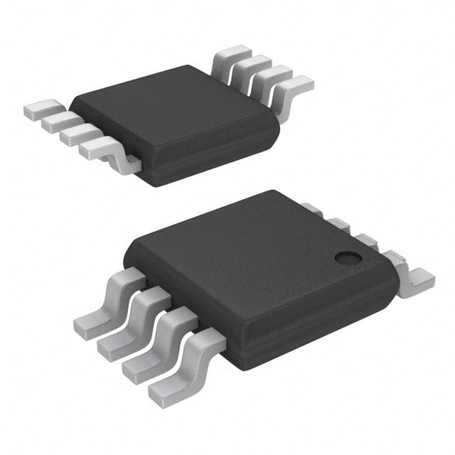
ICGOO在线商城 > 集成电路(IC) > 数据采集 - 模数转换器 > AD7680ARMZ
- 型号: AD7680ARMZ
- 制造商: Analog
- 库位|库存: xxxx|xxxx
- 要求:
| 数量阶梯 | 香港交货 | 国内含税 |
| +xxxx | $xxxx | ¥xxxx |
查看当月历史价格
查看今年历史价格
AD7680ARMZ产品简介:
ICGOO电子元器件商城为您提供AD7680ARMZ由Analog设计生产,在icgoo商城现货销售,并且可以通过原厂、代理商等渠道进行代购。 AD7680ARMZ价格参考¥83.62-¥112.77。AnalogAD7680ARMZ封装/规格:数据采集 - 模数转换器, 16 Bit Analog to Digital Converter 1 Input 1 SAR 8-MSOP。您可以下载AD7680ARMZ参考资料、Datasheet数据手册功能说明书,资料中有AD7680ARMZ 详细功能的应用电路图电压和使用方法及教程。
AD7680ARMZ 是由 Analog Devices Inc.(ADI)生产的一款 16 位、低功耗、逐次逼近寄存器(SAR)模数转换器(ADC)。它属于数据采集 - 模数转换器类别,广泛应用于需要高精度和低功耗的场景。以下是 AD7680ARMZ 的主要应用场景:

 1. 工业自动化与控制
   - 在工业自动化中,AD7680ARMZ 可用于传感器信号采集,例如温度、压力、流量等传感器的数据转换。
   - 它的高精度和低功耗特性非常适合工业现场设备,如可编程逻辑控制器(PLC)、分布式控制系统(DCS)和远程终端单元(RTU)。

 2. 医疗设备
   - 医疗设备对精度要求极高,AD7680ARMZ 可用于心电图(ECG)、血压监测仪、血糖仪等设备中的信号采集。
   - 其低功耗特性有助于延长便携式医疗设备的电池寿命。

 3. 电力监控与能源管理
   - 在电力系统中,AD7680ARMZ 可用于电流、电压和功率的精确测量。
   - 它适用于智能电网、电表和能量管理系统中的数据采集模块。

 4. 测试与测量仪器
   - AD7680ARMZ 被广泛用于数字万用表、示波器和其他测试设备中,提供高分辨率和快速采样能力。
   - 其 SAR 架构确保了稳定的性能和较低的延迟。

 5. 汽车电子
   - 在汽车领域,AD7680ARMZ 可用于电池管理系统(BMS)、发动机控制单元(ECU)以及车载传感器的数据采集。
   - 它能够满足汽车电子对可靠性和精度的要求。

 6. 消费电子
   - 在一些高端消费电子产品中,如音频设备和智能家居控制器,AD7680ARMZ 提供了高质量的信号转换能力。
   - 其紧凑的封装形式(如 ARMZ 封装)适合小型化设计需求。

 7. 物联网(IoT)
   - AD7680ARMZ 的低功耗和高精度特性使其成为 IoT 设备的理想选择,例如环境监测、农业传感和资产跟踪。
   - 它可以将模拟信号高效地转换为数字信号,以便通过无线网络传输。

 总结
AD7680ARMZ 凭借其 16 位分辨率、低功耗和紧凑封装,在工业、医疗、电力、汽车、消费电子和 IoT 等领域具有广泛的应用前景。其出色的性能和可靠性使得它成为高性能数据采集系统的理想选择。
| 参数 | 数值 |
| 产品目录 | 集成电路 (IC)半导体 |
| 描述 | IC ADC 16BIT SRL 100KSPS 8MSOP模数转换器 - ADC 3mW 100kSPS 16-Bit |
| 产品分类 | |
| 品牌 | Analog Devices |
| 产品手册 | |
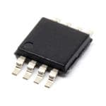
| 产品图片 |
|
| rohs | 符合RoHS无铅 / 符合限制有害物质指令(RoHS)规范要求 |
| 产品系列 | 数据转换器IC,模数转换器 - ADC,Analog Devices AD7680ARMZPulSAR® |
| 数据手册 | |
| 产品型号 | AD7680ARMZ |
| 产品种类 | 模数转换器 - ADC |
| 位数 | 16 |
| 供应商器件封装 | 8-MSOP |
| 信噪比 | 86 dB |
| 分辨率 | 16 bit |
| 包装 | 管件 |
| 商标 | Analog Devices |
| 安装类型 | 表面贴装 |
| 安装风格 | SMD/SMT |
| 封装 | Tube |
| 封装/外壳 | 8-TSSOP,8-MSOP(0.118",3.00mm 宽) |
| 封装/箱体 | MSOP-8 |
| 工作温度 | -40°C ~ 85°C |
| 工作电源电压 | 5 V |
| 工厂包装数量 | 50 |
| 接口类型 | Serial (SPI, QSPI, Microwire) |
| 数据接口 | DSP,MICROWIRE™,QSPI™,串行,SPI™ |
| 最大功率耗散 | 26.4 mW |
| 最大工作温度 | + 85 C |
| 最小工作温度 | - 40 C |
| 标准包装 | 50 |
| 电压参考 | External |
| 电压源 | 单电源 |
| 系列 | AD7680 |
| 结构 | SAR |
| 转换器数 | 1 |
| 转换器数量 | 1 |
| 转换速率 | 100 kS/s |
| 输入数和类型 | 1 个单端,单极 |
| 输入类型 | Single-Ended |
| 通道数量 | 1 Channel |
| 采样率(每秒) | 100k |





- 商务部:美国ITC正式对集成电路等产品启动337调查
- 曝三星4nm工艺存在良率问题 高通将骁龙8 Gen1或转产台积电
- 太阳诱电将投资9.5亿元在常州建新厂生产MLCC 预计2023年完工
- 英特尔发布欧洲新工厂建设计划 深化IDM 2.0 战略
- 台积电先进制程称霸业界 有大客户加持明年业绩稳了
- 达到5530亿美元!SIA预计今年全球半导体销售额将创下新高
- 英特尔拟将自动驾驶子公司Mobileye上市 估值或超500亿美元
- 三星加码芯片和SET,合并消费电子和移动部门,撤换高东真等 CEO
- 三星电子宣布重大人事变动 还合并消费电子和移动部门
- 海关总署:前11个月进口集成电路产品价值2.52万亿元 增长14.8%




PDF Datasheet 数据手册内容提取
3 mW, 100 kSPS, 16-Bit ADC in 6-Lead SOT-23 AD7680 FEATURES FUNCTIONAL BLOCK DIAGRAM Fast throughput rate: 100 kSPS VDD Specified for V of 2.5 V to 5.5 V DD Low power 16-BIT SUCCESSIVE 3 mW typ at 100 kSPS with 2.5 V supply VIN T/H APPROXIMATION ADC 3.9 mW typ at 100 kSPS with 3 V supply 16.7 mW typ at 100 kSPS with 5 V supply SCLK Wide input bandwidth AD7680 CONTROL SDATA 86 dB SNR at 10 kHz input frequency LOGIC CS FNloe xpiibpleel pinoew deerl/asyesr ial clock speed management GND 03643-0-001 High speed serial interface Figure 1. SPI®/QSPI™/μWire/DSP compatible Standby mode: 0.5 μA max 6-Lead SOT-23 and 8-Lead MSOP packages Table 1. MSOP/SOT-23 16-Bit PulSAR ADC APPLICATIONS Type/kSPS 100 kSPS 250 kSPS 500 kSPS Battery-powered systems: True Differential AD7684 AD7687 AD7688 Personal digital assistants Pseudo Differential AD7683 AD7685 AD7686 Medical instruments Unipolar AD7680 Mobile communications Instrumentation and control systems Remote data acquisition systems High speed modems Optical sensors GENERAL DESCRIPTION PRODUCT HIGHLIGHTS The AD7680 is a 16-bit, fast, low power, successive 1. First 16-bit ADC in a SOT-23 package. approximation ADC. The part operates from a single 2.5 V to 2. High throughput with low power consumption. 5.5 V power supply and features throughput rates up to 100 kSPS. The part contains a low noise, wide bandwidth track-and-hold 3. Flexible power/serial clock speed management. The amplifier that can handle input frequencies in excess of 7 MHz. conversion rate is determined by the serial clock, allowing the conversion time to be reduced through the serial clock The conversion process and data acquisition are controlled speed increase. This allows the average power consumption using CS and the serial clock, allowing the devices to interface to be reduced when a power-down mode is used while not with microprocessors or DSPs. The input signal is sampled on converting. The part also features a shutdown mode to the falling edge of CS and the conversion is also initiated at this maximize power efficiency at lower throughput rates. point. There are no pipeline delays associated with the part. Power consumption is 0.5 μA max when in shutdown. The AD7680 uses advanced design techniques to achieve very 4. Reference derived from the power supply. low power dissipation at fast throughput rates. The reference for 5. No pipeline delays. the part is taken internally from V , which allows the widest DD dynamic input range to the ADC. Thus, the analog input range This part features a standard successive approximation ADC for this part is 0 V to VDD. The conversion rate is determined by with accurate control of the sampling instant via a CS input and the SCLK frequency. once-off conversion control. Rev. A Information furnished by Analog Devices is believed to be accurate and reliable. However, no responsibility is assumed by Analog Devices for its use, nor for any infringements of patents or other rights of third parties that may result from its use. One Technology Way, P.O. Box 9106, Norwood, MA 02062-9106, U.S.A. Specifications subject to change without notice. No license is granted by implication or otherwise under any patent or patent rights of Analog Devices. Trademarks and Tel: 781.329.4700 www.analog.com registered trademarks are the property of their respective owners. Fax: 781.326.8703© 2004-2011 Analog Devices, Inc. All rights reserved.
AD7680 TABLE OF CONTENTS Specifications ..................................................................................... 2 Typical Connection Diagram ................................................... 13 Specifications ..................................................................................... 4 Digital Inputs .......................................................................... 13 Timing Specifications ....................................................................... 6 Modes of Operation ....................................................................... 14 Absolute Maximum Ratings ............................................................ 7 Normal Mode .............................................................................. 14 ESD Caution .................................................................................. 7 Power-Down Mode .................................................................... 15 Pin Configurations and Function Descriptions ........................... 8 Power vs. Throughput Rate ........................................................... 16 Terminology ...................................................................................... 9 Serial Interface ................................................................................ 17 Typical Performance Characteristics ........................................... 10 AD7680 to ADSP-218x .............................................................. 18 Circuit Information ........................................................................ 12 Application Hints ........................................................................... 19 Converter Operation .................................................................. 12 Grounding and Layout .............................................................. 19 Analog Input ............................................................................... 12 Outline Dimensions ....................................................................... 20 ADC Transfer Function ................................................................. 13 Ordering Guide .......................................................................... 21 REVISION HISTORY 5/11—Rev. 0 to Rev. A Deleted the Evaluating the AD7680 Performance Section ...... 19 Changes to Ordering Guide .......................................................... 21 1/04—Revision 0: Initial Version Rev. A | Page 2 of 24
AD7680 SPECIFICATIONS1 Table 2. V = 4.5 V to 5.5 V, f = 2.5 MHz, f = 100 kSPS, unless otherwise noted; T = T to T , unless otherwise noted DD SCLK SAMPLE A MIN MAX Parameter A, B Versions1 Unit Test Conditions/Comments DYNAMIC PERFORMANCE f = 10 kHz sine wave IN Signal-to-Noise + Distortion (SINAD)2 83 dB min 85 dB typ Signal-to-Noise Ratio (SNR)2 84 dB min 86 dB typ Total Harmonic Distortion (THD)2 −97 dB typ Peak Harmonic or Spurious Noise (SFDR)2 −95 dB typ Intermodulation Distortion (IMD)2 Second-Order Terms −94 dB typ Third-Order Terms −100 dB typ Aperture Delay 20 ns max Aperture Jitter 30 ps typ Full Power Bandwidth 8 MHz typ @ −3 dB 2.2 MHz typ @ −0.1 dB DC ACCURACY No Missing Codes 15 Bits typ Integral Nonlinearity2 ±4 LSB typ Offset Error2 ±1.68 mV max Gain Error2 ±0.038 % FS max ANALOG INPUT Input Voltage Ranges 0 to V V DD DC Leakage Current ±0.3 μA max Input Capacitance 30 pF typ LOGIC INPUTS Input High Voltage, V 2.8 V min INH Input Low Voltage, V 0.4 V max INL Input Current, I ±0.3 μA max Typically 10 nA, V = 0 V or V IN IN DD Input Capacitance, C 2, 3 10 pF max IN LOGIC OUTPUTS Output High Voltage, V V − 0.2 V min I = 200 μA OH DD SOURCE Output Low Voltage, V 0.4 V max I = 200 μA OL SINK Floating-State Leakage Current ±0.3 μA max Floating-State Output Capacitance2, 3 10 pF max Output Coding Straight (Natural) Binary CONVERSION RATE Conversion Time 8 μs max 20 SCLK cycles with SCLK at 2.5 MHz 9.6 μs max 24 SCLK cycles with SCLK at 2.5 MHz Track-and-Hold Acquisition Time 1.5 μs max 400 ns max Sine wave input ≤ 10 kHz Throughput Rate 100 kSPS See the Serial Interface section POWER REQUIREMENTS V 4.5/5.5 V min/V max DD I Digital I/P = 0 V or V DD S DD Normal Mode (Static) 5.2 mA max SCLK on or off. V = 5.5 V DD Normal Mode (Operational) 4.8 mA max f = 100 kSPS. V = 5.5 V; 3.3 mA typ SAMPLE DD Full Power-Down Mode 0.5 μA max SCLK on or off. V = 5.5 V DD Power Dissipation4 V = 5.5 V DD Normal Mode (Operational) 26.4 mW max f = 100 kSPS SAMPLE Full Power-Down 2.75 μW max 1Temperature range as follows: B Version: −40°C to +85°C. 2 See the Terminology section. 3 Sample tested during initial release to ensure compliance. 4 See the Power vs. Throughput Rate section. Rev. A | Page 3 of 24
AD7680 SPECIFICATIONS1 Table 3. V = 2.5 V to 4.096 V, f = 2.5 MHz, f = 100 kSPS, unless otherwise noted; T = T to T , unless otherwise noted. DD SCLK SAMPLE A MIN MAX Parameter A Version1 B Version1 Unit Test Conditions/Comments DYNAMIC PERFORMANCE f = 10 kHz sine wave IN Signal-to-Noise + Distortion (SINAD)2 83 83 dB min V = 4.096 V DD 82 82 dB min V = 2.5 V to 3.6 V DD 86 86 dB typ Signal-to-Noise Ratio (SNR)2 84 84 dB min V = 4.096 V DD 83 83 dB min V = 2.5 V to 3.6 V DD 86 86 dB typ Total Harmonic Distortion (THD) 2 −98 −98 dB typ Peak Harmonic or Spurious Noise (SFDR)2 −95 −99 dB typ Intermodulation Distortion (IMD)2 Second-Order Terms −94 −94 dB typ Third-Order Terms −100 −100 dB typ Aperture Delay 20 10 ns max Aperture Jitter 30 30 ps typ Full Power Bandwidth 7 7 MHz typ @ −3 dB; V = 4.096 V DD 5 5 MHz typ @ −3 dB; V = 2.5 V to 3.6 V DD 2 2 MHz typ @ −0.1 dB; V = 4.096 V DD 1.6 1.6 MHz typ @ −0.1 dB; V = 2.5 V to 3.6 V DD DC ACCURACY No Missing Codes 14 15 Bits min Integral Nonlinearity2 ±3.5 ±3.5 LSB max V = 4.096 V DD ±3 ±3 LSB max V = 2.5 V to 3.6 V DD Offset Error2 ±1.25 ±1.25 mV max V = 4.096 V DD ±1.098 ±1.098 mV max V = 2.5 V to 3.6 V DD Gain Error2 ±0.038 ±0.038 % FS max ANALOG INPUT Input Voltage Ranges 0 to V 0 to V V DD DD DC Leakage Current ±0.3 ±0.3 μA max Input Capacitance 30 30 pF typ LOGIC INPUTS Input High Voltage, V 2.4 2.4 V min INH Input Low Voltage, V 0.4 0.4 V max INL Input Current, I ±0.3 ±0.3 μA max Typically 10 nA, V = 0 V or V IN IN DD Input Capacitance, C 2, 3 10 10 pF max IN LOGIC OUTPUTS Output High Voltage, V V − 0.2 V − 0.2 V min I = 200 μA OH DD DD SOURCE Output Low Voltage, V 0.4 0.4 V max I = 200 μA OL SINK Floating-State Leakage Current ±0.3 ±0.3 μA max Floating-State Output Capacitance2, 3 10 10 pF max Output Coding Straight (Natural) Binary CONVERSION RATE Conversion Time 8 8 μs max 20 SCLK cycles with SCLK at 2.5 MHz 9.6 9.6 μs max 24 SCLK cycles with SCLK at 2.5 MHz Track-and-Hold Acquisition Time 1.5 1.5 μs max Full-scale step input 400 400 ns max Sine wave input ≤ 10 kHz Throughput Rate 100 100 kSPS See the Serial Interface section Rev. A | Page 4 of 24
AD7680 Parameter A Version1 B Version1 Unit Test Conditions/Comments POWER REQUIREMENTS V 2.5/4.096 2.5/4.096 V min/max DD I Digital I/Ps = 0 V or V DD DD Normal Mode (Static) 2.8 2.8 mA max SCLK on or off; V = 4.096 V DD 2 2 mA max SCLK on or off; V = 3.6 V DD Normal Mode (Operational) 2.6 2.6 mA max f = 100 kSPS; V = 4.096 V; 1.75 mA typ SAMPLE DD 1.9 1.9 mA max f = 100 kSPS; V = 3.6 V; 1.29 mA typ SAMPLE DD Full Power-Down Mode 0.3 0.3 μA max SCLK on or off Power Dissipation4 Normal Mode (Operational) 10.65 10.65 mW max f = 100 kSPS; V = 4.096 V SAMPLE DD 6.84 6.84 mW max f = 100 kSPS; V = 3.6 V SAMPLE DD 3 3 mW typ V = 2.5 V DD Full Power-Down 1.23 1.23 μW max V = 4.096V DD 1.08 1.08 μW max V = 3.6 V DD 1 Temperature range as follows: A, B Versions: −40°C to +85°C. 2 See the Terminology section. 3 Sample tested during initial release to ensure compliance. 4 See the Power vs. Throughput Rate section. Rev. A | Page 5 of 24
AD7680 TIMING SPECIFICATIONS1 Table 4. V = 2.5 V to 5.5 V; T = T to T , unless otherwise noted. DD A MIN MAX Limit at T , T MIN MAX Parameter 3 V 5 V Unit Description f 2 250 250 kHz min SCLK 2.5 2.5 MHz max t 20 × t 20 × t min CONVERT SCLK SCLK t 100 100 ns min Minimum quiet time required between bus relinquish and start of next conversion QUIET t1 10 10 ns min Minimum CS pulse width t2 10 10 ns min CS to SCLK setup time t33 48 35 ns max Delay from CS until SDATA three-state disabled t3 120 80 ns max Data access time after SCLK falling edge 4 t 0.4 t 0.4 t ns min SCLK low pulse width 5 SCLK SCLK t 0.4 t 0.4 t ns min SCLK high pulse width 6 SCLK SCLK t 10 10 ns min SCLK to data valid hold time 7 t 4 45 35 ns max SCLK falling edge to SDATA high impedance 8 t 5 1 1 μs typ Power up time from full power-down POWER-UP 1 Sample tested during initial release to ensure compliance. All input signals are specified with tr = tf = 5 ns (10% to 90% of VDD) and timed from a voltage level of 1.6 V. 2 Mark/space ratio for the SCLK input is 40/60 to 60/40. 3 Measured with the load circuit of Figure 2 and defined as the time required for the output to cross 0.8 V or 2.0 V. 4 t8 is derived form the measured time taken by the data outputs to change 0.5 V when loaded with the circuit of Figure 2. The measured number is then extrapolated back to remove the effects of charging or discharging the 50 pF capacitor. This means that the time, t8, quoted in the timing characteristics is the true bus relinquish time of the part and is independent of the bus loading. 5 See Power vs. Throughput Rate section. 200μA IOL TO OUTPUT 1.6V PIN CL 50pF 200μA IOH 03643-0-002 Figure 2. Load Circuit for Digital Output Timing Specification Rev. A | Page 6 of 24
AD7680 ABSOLUTE MAXIMUM RATINGS Table 5. T = 25°C, unless otherwise noted. A Stresses above those listed under Absolute Maximum Ratings Parameter Rating may cause permanent damage to the device. This is a stress VDD to GND −0.3 V to +7 V rating only; functional operation of the device at these or any Analog Input Voltage to GND −0.3 V to VDD + 0.3 V other conditions above those listed in the operational sections Digital Input Voltage to GND −0.3 V to +7 V of this specification is not implied. Exposure to absolute Digital Output Voltage to GND −0.3 V to VDD + 0.3 V maximum rating conditions for extended periods may affect Input Current to Any Pin Except Supplies1 ±10 mA device reliability. Operating Temperature Range Commercial (B Version) −40°C to +85°C Storage Temperature Range −65°C to +150°C Junction Temperature 150°C SOT-23 Package, Power Dissipation 450 mW θ Thermal Impedance 229.6°C/W JA θ Thermal Impedance 91.99°C/W JC MSOP Package, Power Dissipation 450 mW θ Thermal Impedance 205.9°C/W JA θJC Thermal Impedance 43.74°C/W Lead Temperature, Soldering Vapor Phase (60 secs) 215°C Infared (15 secs) 220°C ESD 2 kV 1Transient currents of up to 100 mA do not cause SCR latch-up. ESD CAUTION ESD (electrostatic discharge) sensitive device. Electrostatic charges as high as 4000 V readily accumulate on the human body and test equipment and can discharge without detection. Although this product features proprietary ESD protection circuitry, permanent damage may occur on devices subjected to high energy electrostatic discharges. Therefore, proper ESD precautions are recommended to avoid performance degradation or loss of functionality. Rev. A | Page 7 of 24
AD7680 PIN CONFIGURATIONS AND FUNCTION DESCRIPTIONS SOT-23 MSOP VDD 1 6 CS VDD 1 8 CS AD7680 AD7680 GFVNigIDNure23 3.( NSToOOtT Pt-o 2V S3IEc PaWilne) Co54nfSSigDCuALrKTaAtio03643-0-003n GGVNNIDDN N234C( =NT oNOtO Pto CV SOIEcNWaNleE)CT765 SNSDCCALKTA03643-0-022 Figure 4. MSOP Pin Configuration Table 6. Pin Function Descriptions Pin No. Pin No. SOT-23 MSOP Mnemonic Function 1 1 VDD Power Supply Input. The VDD range for the AD7680 is from 2.5 V to 5.5 V. 2 2, 3 GND Analog Ground. Ground reference point for all circuitry on the AD7680. All analog input signals should be referred to this GND voltage. 3 4 V Analog Input. Single-ended analog input channel. The input range is 0 V to V . IN DD 4 5 SCLK Serial Clock. Logic input. SCLK provides the serial clock for accessing data from this part. This clock input is also used as the clock source for the AD7680's conversion process. 5 7 SDATA Data Out. Logic output. The conversion result from the AD7680 is provided on this output as a serial data stream. The bits are clocked out on the falling edge of the SCLK input. The data stream from the AD7680 consists of four leading zeros followed by 16 bits of conversion data that are provided MSB first. This will be followed by four trailing zeroes if CS is held low for a total of 24 SCLK cycles. See the Serial Interface section. 6 8 CS Chip Select. Active low logic input. This input provides the dual function of initiating conversions on the AD7680 and framing the serial data transfer. N/A 6 NC No Connect. This pin should be left unconnected. Rev. A | Page 8 of 24
AD7680 TERMINOLOGY Integral Nonlinearity Total Harmonic Distortion (THD) This is the maximum deviation from a straight line passing THD is the ratio of the rms sum of harmonics to the through the endpoints of the ADC transfer function. The fundamental. For the AD7680, it is defined as endpoints of the transfer function are zero scale, a point 1/2 LSB below the first code transition, and full scale, a point V 2+V 2+V 2+V 2+V 2 THD(dB)=20log 2 3 4 5 6 1/2 LSB above the last code transition. V 1 Differential Nonlinearity where V is the rms amplitude of the fundamental and V, V, 1 2 3 This is the difference between the measured and the ideal 1 LSB V, V, and V are the rms amplitudes of the second through the 4 5 6 change between any two adjacent codes in the ADC. sixth harmonics. Offset Error Peak Harmonic or Spurious Noise This is the deviation of the first code transition (00 . . . 000) to Peak harmonic or spurious noise is defined as the ratio of the (00 . . . 001) from the ideal, i.e., AGND + 1 LSB. rms value of the next largest component in the ADC output spectrum (up to f/2, excluding dc) to the rms value of the S Gain Error fundamental. Normally, the value of this specification is This is the deviation of the last code transition (111 . . . 110) to determined by the largest harmonic in the spectrum, but for (111 . . . 111) from the ideal (i.e., V − 1 LSB) after the offset REF ADCs where the harmonics are buried in the noise floor, it is a error has been adjusted out. noise peak. Track-and-Hold Acquisition Time Intermodulation Distortion The track-and-hold amplifier returns to track mode at the end With inputs consisting of sine waves at two frequencies, fa and fb, of conversion. The track-and-hold acquisition time is the time any active device with nonlinearities creates distortion products required for the output of the track-and-hold amplifier to reach at the sum and difference frequencies of mfa ± nfb where m, n = its final value, within ±1 LSB, after the end of the conversion. 0, 1, 2, 3. Intermodulation distortion terms are those for which See the Serial Interface section for more details. neither m nor n are equal to zero. For example, the second-order terms include (fa + fb) and (fa − fb), while the third-order terms Signal-to-(Noise + Distortion) Ratio include (2fa + fb), (2fa − fb), (fa + 2fb), and (fa −2fb). This is the measured ratio of signal-to-(noise + distortion) at the output of the ADC. The signal is the rms amplitude of the The AD7680 is tested using the CCIF standard where two input fundamental. Noise is the sum of all nonfundamental signals up frequencies near the top end of the input bandwidth are used. to half the sampling frequency (f/2, excluding dc). The ratio S In this case, the second-order terms are usually distanced in depends on the number of quantization levels in the digitization frequency from the original sine waves, while the third-order process; the more levels, the smaller the quantization noise. The terms are usually at a frequency close to the input frequencies. theoretical signal-to-(noise + distortion) ratio for an ideal N-bit As a result, the second- and third-order terms are specified converter with a sine wave input is given by separately. The calculation of the intermodulation distortion is as per the THD specification where it is the ratio of the rms Signal-to-(Noise + Distortion) = (6.02 N + 1.76) dB sum of the individual distortion products to the rms amplitude Thus, for a 16-bit converter, this is 98 dB. of the sum of the fundamentals expressed in dBs. Rev. A | Page 9 of 24
AD7680 TYPICAL PERFORMANCE CHARACTERISTICS Figure 5 shows a typical FFT plot for the AD7680 at 100 kSPS Figure 7 shows a graph of the total harmonic distortion versus sample rate and 10 kHz input frequency. Figure 6 shows the the analog input frequency for various supply voltages, while signal-to-(noise + distortion) ratio performance versus the Figure 8 shows a graph of the total harmonic distortion versus input frequency for various supply voltages while sampling at the analog input frequency for various source impedances (see 100 kSPS with an SCLK of 2.5 MHz. the Analog Input section). Figure 9 and Figure 10 show the typical INL and DNL plots for the AD7680. 0 110 VDD = 5V FSAMPLE = 100kSPS –20 FFSINA =M P1L0Ek H= z100kSPS TA = 25°C SNR = 88.28dB –40 SINAD = 87.82dB 105 THD =–97.76dB VDD = 4.3V SFDR =–98.25dB –60 VDD = 4.75V dB –80 HD (dB) 100 VVDDDD == 35..62V5V T –100 VDD = 3.0V VDD = 2.7V –120 95 VDD = 2.5V ––114600 03643-0-021 90 03643-0-017 0 10k 20k 30k 40k 50k 10 100 FREQUENCY (kHz) INPUT FREQUENCY (kHz) Figure 5. AD7680 Dynamic Performance at 100 kSPS Figure 7. AD7680 THD vs. Analog Input Frequency for Various Supply Voltages at 100 kSPS 95 110 TFSAA =M 2P5L°EC = 100kSPS RIN = 10Ω 105 100 90 RIN = 50Ω B) VDD = 5.25V B) 95 SINAD (d VDD = 4.75V THD (d 90 RIN = 100Ω 85 VDD = 4.3V 85 VDD = 3.6V 80 VDD = 2.5V VVDDDD == 32..07VV 03643-0-016 785010TFVSADA D=M =2P 54L°E.7C =5 V100kSPS RIN = 1000Ω 10003643-0-018 10 100 INPUT FREQUENCY (kHz) INPUT FREQUENCY (kHz) Figure 6. AD7680 SINAD vs. Analog Input Frequency Figure 8. AD7680 THD vs. Analog Input Frequency for Various Supply Voltages at 100 kSPS for Various Source Impedances Rev. A | Page 10 of 24
AD7680 2.5 1.5 TVEDDM P= 3=. 02V5°C TVEDDM P= 3=. 02V5°C 2.0 1.0 1.5 B) B) 0.5 R (LS 1.0 R (LS O O 0 R R INL ER 0.5 DNL ER–0.5 0 –1.0 ––10..05 03643-0-019 –1.5 03643-0-020 0 10000 20000 30000 40000 50000 60000 70000 0 10000 20000 30000 40000 50000 60000 70000 CODE CODE Figure 9. AD7680 Typical INL Figure 10. AD7680 Typical DNL Rev. A | Page 11 of 24
AD7680 CIRCUIT INFORMATION The AD7680 is a fast, low power, 16-bit, single-supply ADC. The CAPACITIVE part can be operated from a 2.5 V to 5.5 V supply and is capable of DAC throughput rates of 100 kSPS when provided with a 2.5 MHz clock. A SAMPLING VIN CAPACITOR SW1 The AD7680 provides the user with an on-chip track-and-hold B CONTROL ApaDckCa gane do ra isne raina l8 i-nleteardf aMceS hOoPu pseadc kinag ae ,t iwnhy i6c-hl eoafdfe Sr OthTe- 2u3se r CONVPDVHDEA/R2SSEION SW2 COMPARATOR LOGIC 03643-0-005 considerable space-saving advantages over alternative solutions. Figure 12. ADC Conversion Phase The serial clock input accesses data from the part and also provides the clock source for the successive approximation ANALOG INPUT ADC. The analog input range for the AD7680 is 0 V to V . An DD Figure 13 shows an equivalent circuit of the analog input external reference is not required for the ADC nor is there a structure of the AD7680. The two diodes, D1 and D2, provide reference on-chip. The reference for the AD7680 is derived from ESD protection for the analog inputs. Care must be taken to the power supply and thus gives the widest dynamic input range. ensure that the analog input signal never exceeds the supply rails by more than 300 mV. This causes these diodes to become The AD7680 also features a power-down option to save power forward-biased and to start conducting current into the between conversions. The power-down feature is implemented substrate. The maximum current these diodes can conduct across the standard serial interface as described in the Modes of without causing irreversible damage to the part is 10 mA. Operation section. Capacitor C1 in Figure 13 is typically about 5 pF and can be CONVERTER OPERATION attributed primarily to pin capacitance. Resistor R1 is a lumped component made up of the on resistance of a track-and-hold The AD7680 is a 16-bit, successive approximation ADC based switch. This resistor is typically about 25 Ω. Capacitor C2 is the around a capacitive DAC. The AD7680 can convert analog ADC sampling capacitor and has a capacitance of 25 pF input signals in the 0 V to V range. Figure 11 and Figure 12 DD typically. For ac applications, removing high frequency show simplified schematics of the ADC. The ADC comprises components from the analog input signal is recommended by control logic, SAR, and a capacitive DAC. Figure 11 shows the use of an RC low-pass filter on the relevant analog input pin. In ADC during its acquisition phase. SW2 is closed and SW1 is in applications where harmonic distortion and signal-to-noise Position A. The comparator is held in a balanced condition and ratio are critical, the analog input should be driven from a low the sampling capacitor acquires the signal on the selected V IN impedance source. Large source impedances significantly affect channel. the ac performance of the ADC. This may necessitate the use of an input buffer amplifier. The choice of the op amp is a function CAPACITIVE DAC of the particular application. When no amplifier is used to drive A SAMPLING the analog input, the source impedance should be limited to low VIN CAPACITOR SW1 values. The maximum source impedance depends on the B CONTROL ACVQPDUHDIAS/2SITEION SW2 COMPARATOR LOGIC 03643-0-004 atinomlceroreuaatnseted so., f Ta tnhodeta Tpl eHhrafDrom rimnocnarniecca dese idsste oagsrr tatihodene s s( o(TsuHerecD eF )ii gmtuhpraeet dc8aa)n.n c bee Figure 11. ADC Acquisition Phase VDD When the ADC starts a conversion, SW2 opens and SW1 moves C2 to Position B, causing the comparator to become unbalanced D1 R1 25pF VIN (Figure 12). The control logic and the capacitive DAC are used C1 D2 tcoa paadcdit aonr dto s ubbritnragc tth feix ceodm apmaorautnotrs boafc ckh ianrtgoe af rboamla nthcee ds ampling 5pF CTROANCVKE RPSHIAOSNE P -H SAWSIET C- HSW CILTOCSHE ODPEN 03643-0-006 condition. When the comparator is rebalanced, the conversion Figure 13. Equivalent Analog Input Circuit is complete. The control logic generates the ADC output code (see the ADC Transfer Function section). Rev. A | Page 12 of 24
AD7680 ADC TRANSFER FUNCTION The output coding of the AD7680 is straight binary. The In fact, because the supply current required by the AD7680 is so designed code transitions occur at successive integer LSB low, a precision reference can be used as the supply source to values, i.e., 1 LSB, 2 LSBs. The LSB size is V /65536. The ideal the AD7680. For example, a REF19x voltage reference (REF195 DD transfer characteristic for the AD7680 is shown in Figure 14. for 5 V or REF193 for 3 V) or an AD780 can be used to supply the required voltage to the ADC (see Figure 15). This configuration is especially useful if the power supply available is quite noisy, or if the system supply voltages are at some value 111...111 111...110 other than the required operating voltage of the AD7680, e.g., 15 V. The REF19x or AD780 outputs a steady voltage to the AD7680. Recommended decoupling capacitors are a 100 nF low 111...000 1 LSB = VDD/65536 ESR ceramic (Farnell 335-1816) and a 10 μF low ESR tantalum 011...111 (Farnell 197-130). 3V 5V REF193 SUPPLY 000...010 T1A0NFT 0.1F 10F 0.1F 000...001 000...000 0V 1 LSB ANALOG INPUT +VDD–1 LSB 03643-0-007 0V TION PVUDTD VINVDD AD7680 SDSACTLAK C/P Figure 14. AD7680 Transfer Characteristic CS TYPICAL CONNECTION DIAGRAM GND FViRgEuF ries 1ta5k sehno iwntse ar ntyaplliyc afrlo cmon VneDDc taionnd dasia sgurcahm s fhooru tlhde b Ae Dw7e6ll8 0. INTESREFRAICAEL 03643-0-008 decoupled. This provides an analog input range of 0 V to V . DD Figure 15. Typical Connection Diagram The conversion result is output in a 24-bit word, or alternatively, Digital Inputs all 16 bits of the conversion result may be accessed using a The digital inputs applied to the AD7680 are not limited by the minimum of 20 SCLKs. This 20-/24-bit data stream consists of maximum ratings that limit the analog inputs. Instead, the a four leading zeros, followed by the 16 bits of conversion data, digital inputs applied can go to 7 V and are not restricted by the followed by four trailing zeros in the case of the 24 SCLK V + 0.3 V limit as on the analog inputs. For example, if the transfer. For applications where power consumption is of DD AD7680 were operated with a V of 3 V, 5 V logic levels could concern, the power-down mode should be used between DD be used on the digital inputs. However, it is important to note conversions or bursts of several conversions to improve power that the data output on SDATA still has 3 V logic levels when performance (see the Modes of Operation section). V = 3 V. DD Another advantage of SCLK and CS not being restricted by the V + 0.3 V limit is that power supply sequencing issues are DD avoided. If one of these digital inputs is applied before V , then DD there is no risk of latch-up as there would be on the analog inputs if a signal greater than 0.3 V were applied prior to V . DD Rev. A | Page 13 of 24
AD7680 MODES OF OPERATION The mode of operation of the AD7680 is selected by controlling The conversion is initiated on the falling edge of CS as described the (logic) state of the CS signal during a conversion. There are in the Serial Interface section. To ensure that the part remains two possible modes of operation, normal and power-down. The fully powered up at all times, CS must remain low until at least point at which CS is pulled high after the conversion has been 10 SCLK falling edges have elapsed after the falling edge of CS. initiated determines whether or not the AD7680 enters power- If CS is brought high any time after the 10th SCLK falling edge, down mode. Similarly, if the AD7680 is already in power-down, but before the 20th SCLK falling edge, the part remains CS can control whether the device returns to normal operation powered up, but the conversion is terminated and SDATA goes or remains in power-down. These modes of operation are back into three-state. At least 20 serial clock cycles are required designed to provide flexible power management options. These to complete the conversion and access the complete conversion options can optimize the power dissipation/throughput rate result. In addition, a total of 24 SCLK cycles accesses four ratio for differing application requirements. trailing zeros. CS may idle high until the next conversion or may idle low until CS returns high sometime prior to the next NORMAL MODE conversion, effectively idling CS low. This mode provides the fastest throughput rate performance, because the user does not have to worry about the power-up Once a data transfer is complete (SDATA has returned to three- times with the AD7680 remaining fully powered all the time. state), another conversion can be initiated after the quiet time, Figure 16 shows the general diagram of the operation of the t , has elapsed by bringing CS low again. QUIET AD7680 in this mode. CS 1 10 20 SCLK SDATA 4 LEADING ZEROS + CONVERSION RESULT 03643-0-009 Figure 16. Normal Mode Operation Rev. A | Page 14 of 24
AD7680 POWER-DOWN MODE This mode is intended for use in applications where slower In order to exit this mode of operation and power up the throughput rates are required. Either the ADC is powered AD7680 again, a dummy conversion is performed. On the down between each conversion, or a series of conversions may falling edge of CS, the device begins to power up and continues be performed at a high throughput rate, and then the ADC is to power up as long as CS is held low until after the falling edge powered down for a relatively long duration between these of the 10th SCLK. The device is fully powered up once at least bursts of several conversions. When the AD7680 is in 16 SCLKs (or approximately 6 μs) have elapsed and valid data power-down, all analog circuitry is powered down. results from the next conversion as shown in Figure 18. If CS is brought high before the 10th falling edge of SCLK, regardless of To enter power-down, the conversion process must be the SCLK frequency, the AD7680 goes back into power-down interrupted by bringing CS high anywhere after the second again. This avoids accidental power-up due to glitches on the falling edge of SCLK and before the 10th falling edge of SCLK CS line or an inadvertent burst of 8 SCLK cycles while CS is low. as shown in Figure 17. Once CS has been brought high in this So although the device may begin to power-up on the falling window of SCLKs, the part enters power-down, the conversion edge of CS, it powers down again on the rising edge of CS as that was initiated by the falling edge of CS is terminated, and long as it occurs before the 10th SCLK falling edge. SDATA goes back into three-state. If CS is brought high before the second SCLK falling edge, the part remains in normal mode and will not power down. This avoids accidental power-down due to glitches on the CS line. CS 1 2 10 20 SCLK SDATA THREE-STATE 03643-0-010 Figure 17. Entering Power-Down Mode THE PART IS FULLY POWERED UP WITH VIN FULLY ACQUIRED THE PART BEGINS TO POWER UP t POWER UP CS 1 10 20 1 20 SCLK SDATA INVALID DATA VALID DATA 03643-0-011 Figure 18. Exiting Power-Down Mode Rev. A | Page 15 of 24
AD7680 POWER VS. THROUGHPUT RATE By using the power-down mode on the AD7680 when not Figure 19 shows the power dissipation versus the throughput converting, the average power consumption of the ADC rate when using the power-down mode with 3.6 V supplies, a decreases at lower throughput rates. Figure 19 shows how as the 2.5 MHz SCLK, and a 20 SCLK serial transfer. throughput rate is reduced, the part remains in its shut-down 10 state longer, and the average power consumption over time VDD = 3.6V FSCLK = 2.5MHz drops accordingly. For example, if the AD7680 is operated in a continuous sampling mode, with a throughput rate of 10 kSPS and an SCLK 1 W) dofo 2w.n5 MmoHdze ( bVeDtDw =ee 3n. 6c oVn)v, earnsdio tnhse, tdheev picoew ise rp lcaocnesdu imn pptoiowne ris- ER (m W calculated as follows. The maximum power dissipation during O P 0.1 normal operation is 6.84 mW (V = 3.6 V). If the power-up DD time from power-down is 1 μs, and the remaining conversion tbiem sea iids 8to μ ds,i s(suipsiantge a6 .2804 SmCWLK f otrr a9n μsfse dr)u, rtihnegn e tahceh A coDn7v6e8r0si coann 0.01 03643-0-012 cycle. With a throughput rate of 10 kSPS, the cycle time is 100 0 5 10 15 20 25 30 35 40 45 50 μs. THROUGHPUT (kSPS) For the remainder of the conversion cycle, 91 μs, the part Figure 19. Power vs. Throughput Using remains in power-down mode. The AD7680 can be said to Power-Down Mode with 20 SCLK Transfer at 3.6 V dissipate 1.08 μW for the remaining 91 μs of the conversion cycle. Therefore, with a throughput rate of 10 kSPS, the average power dissipated during each cycle is (9/100) × (6.84 mW) + (91/100) × (1.08 μW) = 0.62 mW Rev. A | Page 16 of 24
AD7680 SERIAL INTERFACE Figure 20 shows the detailed timing diagram for serial A minimum of 20 serial clock cycles are required to perform interfacing to the AD7680. The serial clock provides the the conversion process and to access data from the AD7680. conversion clock and also controls the transfer of information CS going low provides the first leading zero to be read in by the from the AD7680 during conversion. microcontroller or DSP. The remaining data is then clocked out by subsequent SCLK falling edges beginning with the second The CS signal initiates the data transfer and conversion process. leading zero; thus the first falling clock edge on the serial clock The falling edge of CS puts the track-and-hold into hold mode, has the first leading zero provided and also clocks out the takes the bus out of three-state, and samples the analog input. second leading zero. If a 24 SCLK transfer is used as in Figure 20, The conversion is also initiated at this point and requires at least the data transfer consists of four leading zeros followed by the 20 SCLK cycles to complete. Once 17 SCLK falling edges have 16 bits of data, followed by four trailing zeros. The final bit elapsed, the track-and-hold goes back into track mode on the (fourth trailing zero) in the data transfer is valid on the 24th next SCLK rising edge. Figure 20 shows a 24 SCLK transfer that falling edge, having been clocked out on the previous (23rd) allows a 100 kSPS throughput rate. On the 24th SCLK falling falling edge. If a 20 SCLK transfer is used as shown in Figure 21, edge, the SDATA line goes back into three-state. If the rising the data output stream consists of only four leading zeros edge of CS occurs before 24 SCLKs have elapsed, the conversion followed by 16 bits of data with the final bit valid on the 20th terminates and the SDATA line goes back into three-state; SCLK falling edge. A 20 SCLK transfer allows for a shorter cycle otherwise SDATA returns to three-state on the 24th SCLK time and therefore a faster throughput rate is achieved. falling edge as shown in Figure 20. t 1 CS t CONVERT t2 t6 1 2 3 4 5 18 19 20 21 22 23 24 SCLK t3 t4 t5 t7 t8 t QUIET SDATA 3-STATE 0 Z4E RLEOADINZGE ZREOROSZERO DB15 DB1 DB0 ZERO 4Z TERRAOILINGZ ZEERROOS ZERO 3-STATE 03643-0-013 Figure 20. AD7680 Serial Interface Timing Diagram—24 SCLK Transfer t 1 CS t CONVERT t t 2 6 SCLK 1 2 3 4 5 18 19 20 t3 t4 t5 t7 tQtU8IET SDATA 3-STATE 0 ZE4 RLOEADINZGE RZEOROSZERO DB15 DB1 DB0 0 3-STATE 03643-0-014 Figure 21. AD7680 Serial Interface Timing Diagram—20 SCLK Transfer Rev. A | Page 17 of 24
AD7680 It is also possible to take valid data on each SCLK rising edge an input. The DSP operates in alternate framing mode and the rather than falling edge, since the SCLK cycle time is long SPORT control register is set up as described. Transmit and enough to ensure the data is ready on the rising edge of SCLK. receive autobuffering is used in order to get a 24 SCLK transfer. However, the first leading zero is still driven by the CS falling Each buffer contains three 8-bit words. The frame synchroniza- edge, and so it can be taken on only the first SCLK falling edge. tion signal generated on the TFS is tied to CS, and as with all It may be ignored and the first rising edge of SCLK after the CS signal processing applications, equidistant sampling is necessary. falling edge would have the second leading zero provided and In this example, the timer interrupt is used to control the the 23rd rising SCLK edge would have the final trailing zero sampling rate of the ADC. provided. This method may not work with most microcontrollers/DSPs but could possibly be used with FPGAs AD7680* ADSP-218x* and ASICs. SCLK SCLK SDATA DR AD7680 TO ADSP-218x TAhDe7 A68D0S wP-it2h1o8uxt faanmyi lgyl uoef lDogSPics rceaqnu ibree din. tTehrfea cSePdO dRiTre cctolny ttroo lt he CS RTFFSS 03643-0-015 *ADDITIONAL PINS OMITTED FOR CLARITY register should be set up as follows: Figure 22. Interfacing to the ADSP-218x TFSW = RFSW = 1, Alternate Framing The timer register is loaded with a value that provides an INVRFS = INVTFS = 1, Active Low Frame Signal interrupt at the required sample interval. When an interrupt is received, the values in the transmit autobuffer start to be DTYPE = 00, Right Justify Data transmitted and TFS is generated. The TFS is used to control SLEN = 0111, 8-Bit Data-Words the RFS and therefore the reading of data. The data is stored in the receive autobuffer for processing or to be shifted later. The ISCLK = 1, Internal Serial Clock frequency of the serial clock is set in the SCLKDIV register. When the instruction to transmit with TFS is given, i.e., TFSR = RFSR = 0, Frame First Word TX0 = AX0, the state of the SCLK is checked. The DSP waits IRFS = 0 until the SCLK has gone high, low, and high again before transmission starts. If the timer and SCLK values are chosen ITFS = 1 such that the instruction to transmit occurs on or near the rising edge of SCLK, the data may be transmitted or it may wait To implement the power-down mode, SLEN should be set to until the next clock edge. 0111 to issue an 8-bit SCLK burst. The connection diagram is shown in Figure 22. The ADSP-218x has the TFS and RFS of the SPORT tied together, with TFS set as an output and RFS set as Rev. A | Page 18 of 24
AD7680 APPLICATION HINTS GROUNDING AND LAYOUT as clocks, should be shielded with digital ground to avoid radiating noise to other sections of the board, and clock signals The printed circuit board that houses the AD7680 should be should never be run near the analog inputs. Avoid crossover of designed such that the analog and digital sections are separated digital and analog signals. Traces on opposite sides of the board and confined to certain areas of the board. This facilitates the should run at right angles to each other, which reduces the use of ground planes that can be separated easily. A minimum effects of feedthrough on the board. A microstrip technique is etch technique is generally best for ground planes, because it by far the best but is not always possible with a double-sided gives the best shielding. Digital and analog ground planes board. In this technique, the component side of the board is should be joined at only one place. If the AD7680 is in a system dedicated to ground planes while the signals are placed on the where multiple devices require an AGND to DGND solder side. connection, the connection should still be made at one point only, a star ground point that should be established as close as Good decoupling is also very important. All analog supplies possible to the AD7680. should be decoupled with 10 μF tantalum in parallel with 0.1 μF capacitors to AGND, as discussed in the Typical Avoid running digital lines under the device because these Connection Diagram section. To achieve the best performance couple noise onto the die. The analog ground plane should be from these decoupling components, the user should attempt to allowed to run under the AD7680 to avoid noise coupling. The keep the distance between the decoupling capacitors and the power supply lines to the AD7680 should use as large a trace as V and GND pins to a minimum, with short track lengths DD possible to provide low impedance paths and reduce the effects connecting the respective pins. of glitches on the power supply line. Fast switching signals, such Rev. A | Page 19 of 24
AD7680 OUTLINE DIMENSIONS 3.00 2.90 2.80 1.70 6 5 4 3.00 1.60 2.80 1.50 2.60 1 2 3 PIN1 INDICATOR 0.95BSC 1.90 BSC 1.30 1.15 0.90 1.45MAX 0.20MAX 0.95MIN 0.08MIN 0.55 00..1055MMAINX 0.50MAX SPELAATNIENG 140°° B0S.6C0 00..4355 0.30MIN 0° COMPLIANTTOJEDECSTANDARDSMO-178-AB 12-16-2008-A Figure 23. 6-Lead Small Outline Transistor Package [SOT-23] (RJ-6) Dimensions shown in millimeters 3.20 3.00 2.80 8 5 5.15 3.20 4.90 3.00 4.65 2.80 1 4 PIN1 IDENTIFIER 0.65BSC 0.95 15°MAX 0.85 1.10MAX 0.75 0.80 CO00P..10L550A.1N0ARICTOYMPLIANT00..T4205OJEDECSTA60°°NDARDS00M..20O39-187-AA 00..5450 10-07-2009-B Figure 24. 8-Lead Micro Small Outline Package [MSOP] (RM-8) Dimensions shown in millimeters Rev. A | Page 20 of 24
AD7680 ORDERING GUIDE Temperature Linearity Package Model1 Range Error (LSB)2 Package Description Option Branding AD7680ARJZ-REEL7 −40°C to +85°C 14 Bits Min 6-Lead Small Outline Transistor Package (SOT-23) RJ-6 C40 AD7680ARM −40°C to +85°C 14 Bits Min 8-Lead Mini Small Outline Package (MSOP) RM-8 CQA AD7680ARM-REEL −40°C to +85°C 14 Bits Min 8-Lead Mini Small Outline Package (MSOP) RM-8 CQA AD7680ARM-REEL7 −40°C to +85°C 14 Bits Min 8-Lead Mini Small Outline Package (MSOP) RM-8 CQA AD7680ARMZ −40°C to +85°C 14 Bits Min 8-Lead Mini Small Outline Package (MSOP) RM-8 C40 AD7680BRJZ-R2 −40°C to +85°C 15 Bits Min 6-Lead Small Outline Transistor Package (SOT-23) RJ-6 C3H AD7680BRJZ-REEL7 −40°C to +85°C 15 Bits Min 6-Lead Small Outline Transistor Package (SOT-23) RJ-6 C3H AD7680BRM −40°C to +85°C 15 Bits Min 8-Lead Mini Small Outline Package (MSOP) RM-8 CQB AD7680BRM-REEL −40°C to +85°C 15 Bits Min 8-Lead Mini Small Outline Package (MSOP) RM-8 CQB AD7680BRM-REEL7 −40°C to +85°C 15 Bits Min 8-Lead Mini Small Outline Package (MSOP) RM-8 CQB AD7680BRMZ −40°C to +85°C 15 Bits Min 8-Lead Mini Small Outline Package (MSOP) RM-8 C3H AD7680BRMZ-REEL −40°C to +85°C 15 Bits Min 8-Lead Mini Small Outline Package (MSOP) RM-8 C3H AD7680BRMZ-REEL7 −40°C to +85°C 15 Bits Min 8-Lead Mini Small Outline Package (MSOP) RM-8 C3H 1 Z = RoHS Compliant Part. 2 Linearity error here refers to no missing codes. Rev. A | Page 21 of 24
AD7680 NOTES Rev. A | Page 22 of 24
AD7680 NOTES Rev. A | Page 23 of 24
AD7680 NOTES © 2004-2011 Analog Devices, Inc. All rights reserved. Trademarks and registered trademarks are the property of their respective owners. D03643-0-5/11(A) Rev. A | Page 24 of 24
Mouser Electronics Authorized Distributor Click to View Pricing, Inventory, Delivery & Lifecycle Information: A nalog Devices Inc.: AD7680BRM-REEL AD7680ARJZ-REEL7 AD7680BRMZ-REEL AD7680ARM-REEL7 AD7680BRMZ AD7680BRM- REEL7 AD7680BRM AD7680BRJZ-REEL7 AD7680ARMZ AD7680ARM AD7680ARM-REEL AD7680BRMZ-REEL7
 Datasheet下载
