ICGOO在线商城 > 集成电路(IC) > 数据采集 - 数模转换器 > AD7397ARUZ
 Datasheet下载
- 型号: AD7397ARUZ
- 制造商: Analog
- 库位|库存: xxxx|xxxx
- 要求:
| 数量阶梯 | 香港交货 | 国内含税 |
| +xxxx | $xxxx | ¥xxxx |
查看当月历史价格
查看今年历史价格
AD7397ARUZ产品简介:
ICGOO电子元器件商城为您提供AD7397ARUZ由Analog设计生产,在icgoo商城现货销售,并且可以通过原厂、代理商等渠道进行代购。 AD7397ARUZ价格参考¥43.66-¥43.66。AnalogAD7397ARUZ封装/规格:数据采集 - 数模转换器, 10 位 数模转换器 2 24-TSSOP。您可以下载AD7397ARUZ参考资料、Datasheet数据手册功能说明书,资料中有AD7397ARUZ 详细功能的应用电路图电压和使用方法及教程。
Analog Devices Inc.的AD7397ARUZ是一款12位、双通道、电压输出型数模转换器(DAC),具有低功耗、高精度和快速建立时间的特点。该器件广泛应用于需要高精度模拟信号生成的场合,适用于工业控制、仪器仪表、通信系统和消费电子等多个领域。

在工业自动化领域,AD7397ARUZ可用于PLC(可编程逻辑控制器)和智能传感器中,实现对控制信号的精确输出。在测试测量设备中,如示波器、信号发生器和分析仪器,该DAC可用于生成高精度的参考信号或校准信号。

此外,AD7397ARUZ也适用于音频处理、电源管理和医疗设备等对信号质量要求较高的应用。其双通道输出特性使其能够同时控制两个独立的模拟信号,提高了系统集成度和控制灵活性。

总之,AD7397ARUZ凭借其高性能和多通道优势,广泛应用于需要精密模拟信号控制和处理的各种电子系统中。
| 参数 | 数值 |
| 产品目录 | 集成电路 (IC)半导体 |
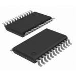
| 描述 | IC DAC 10BIT PARALLEL 3V 24TSSOP数模转换器- DAC Dual Parallel-Input 10-Bit |
| 产品分类 | |
| 品牌 | Analog Devices |
| 产品手册 | |
| 产品图片 |
|
| rohs | 符合RoHS无铅 / 符合限制有害物质指令(RoHS)规范要求 |
| 产品系列 | 数据转换器IC,数模转换器- DAC,Analog Devices AD7397ARUZ- |
| 数据手册 | |
| 产品型号 | AD7397ARUZ |
| 产品培训模块 | http://www.digikey.cn/PTM/IndividualPTM.page?site=cn&lang=zhs&ptm=19145http://www.digikey.cn/PTM/IndividualPTM.page?site=cn&lang=zhs&ptm=18614http://www.digikey.cn/PTM/IndividualPTM.page?site=cn&lang=zhs&ptm=26125http://www.digikey.cn/PTM/IndividualPTM.page?site=cn&lang=zhs&ptm=26140http://www.digikey.cn/PTM/IndividualPTM.page?site=cn&lang=zhs&ptm=26150http://www.digikey.cn/PTM/IndividualPTM.page?site=cn&lang=zhs&ptm=26147 |
| 产品种类 | 数模转换器- DAC |
| 位数 | 10 |
| 供应商器件封装 | 24-TSSOP |
| 分辨率 | 10 bit |
| 包装 | 管件 |
| 商标 | Analog Devices |
| 安装类型 | 表面贴装 |
| 安装风格 | SMD/SMT |
| 封装 | Tube |
| 封装/外壳 | 24-TSSOP(0.173",4.40mm 宽) |
| 封装/箱体 | TSSOP-24 |
| 工作温度 | -40°C ~ 125°C |
| 工厂包装数量 | 62 |
| 建立时间 | 60µs |
| 接口类型 | Parallel |
| 数据接口 | 并联 |
| 最大功率耗散 | 1 mW |
| 最大工作温度 | + 125 C |
| 最小工作温度 | - 40 C |
| 标准包装 | 62 |
| 电压参考 | External |
| 电压源 | 单电源 |
| 电源电压-最大 | 5.5 V |
| 电源电压-最小 | 2.7 V |
| 积分非线性 | +/- 2 LSB |
| 稳定时间 | 60 us |
| 系列 | AD7397 |
| 结构 | R-2R |
| 转换器数 | 2 |
| 转换器数量 | 2 |
| 输出数和类型 | 2 电压,单极2 电压,双极 |
| 输出类型 | Voltage |
| 采样比 | 17 kSPs |
| 采样率(每秒) | 17k |


- 商务部:美国ITC正式对集成电路等产品启动337调查
- 曝三星4nm工艺存在良率问题 高通将骁龙8 Gen1或转产台积电
- 太阳诱电将投资9.5亿元在常州建新厂生产MLCC 预计2023年完工
- 英特尔发布欧洲新工厂建设计划 深化IDM 2.0 战略
- 台积电先进制程称霸业界 有大客户加持明年业绩稳了
- 达到5530亿美元!SIA预计今年全球半导体销售额将创下新高
- 英特尔拟将自动驾驶子公司Mobileye上市 估值或超500亿美元
- 三星加码芯片和SET,合并消费电子和移动部门,撤换高东真等 CEO
- 三星电子宣布重大人事变动 还合并消费电子和移动部门
- 海关总署:前11个月进口集成电路产品价值2.52万亿元 增长14.8%


PDF Datasheet 数据手册内容提取
a 3 V, Parallel Input Dual 12-Bit/10-Bit DACs AD7396/AD7397 FEATURES FUNCTIONAL BLOCK DIAGRAM Micropower: 100 mA/DAC 0.1 mA Typical Power Shutdown Single Supply +2.7 V to +5.5 V Operation AD7396 VDD DACA 12 12-BIT Compact 1.1 mm Height TSSOP 24-Lead Package LDA REGISTER DACA VOUTA AD7396: 12-Bit Resolution AD7397: 10-Bit Resolution CS INPUTA 0.9 LSB Differential Nonlinearity Error A/B REGISTER APPLICATIONS DATA 12 1 VREF Automotive Output Span Voltage INPUTB Portable Communications REGISTER Digitally Controlled Calibration DACB 12 12-BIT PC Peripherals LDB REGISTER DACB VOUTB AGND DGND RS SHDN GENERAL DESCRIPTION Both parts are offered in the same pinout, allowing users to The AD7396/AD7397 series of dual, 12-bit and 10-bit voltage- select the amount of resolution appropriate for their applications output digital-to-analog converters are designed to operate from without circuit card changes. a single +3 V supply. Built using a CBCMOS process, these The AD7396/AD7397 are specified for operation over the ex- monolithic DACs offer the user low cost and ease of use in tended industrial (–40(cid:176) C to +85(cid:176) C) temperature range. The single supply +3 V systems. Operation is guaranteed over the AD7397AR is specified for the –40(cid:176) C to +125(cid:176) C automotive supply voltage range of +2.7 V to +5.5 V, making this device temperature range. AD7396/AD7397s are available in plastic ideal for battery operated applications. DIP, and 24-lead SOIC packages. The AD7397ARU is avail- A 12-bit wide data latch loads with a 45 ns write time allowing able for ultracompact applications in a thin 1.1 mm height interface to fast processors without wait states. The double TSSOP 24-lead package. buffered input structure allows the user to load the input registers one at a time, then a single load strobe tied to both 1.0 LDA+LDB inputs will simultaneously update both DAC out- VDD = +3V puts. LDA and LDB can also be independently activated to 0.8 VREF = +2.5V immediately update their respective DAC registers. An address 0.6 input (A/B) decodes DACA or DACB when the chip select CS 0.4 input is strobed. Additionally, an asynchronous RS input sets B 0.2 the output to zero-scale at power on or upon user demand. S L Power shutdown to submicroamp levels is directly controlled by L – 0.0 N the active low SHDN pin. While in the power shutdown state D–0.2 register data can still be changed even though the output buffer –0.4 is in an open circuit state. Upon return to the normal operating TA = +258C, +858C, –558C state the latest data loaded in the DAC register will establish the –0.6 SUPERIMPOSED output voltage. –0.8 –1.0 0 512 1024 1536 2048 2560 3072 3584 4096 CODE – Decimal Figure 1.DNL vs. Digital Code at Temperature REV.0 Information furnished by Analog Devices is believed to be accurate and reliable. However, no responsibility is assumed by Analog Devices for its use, nor for any infringements of patents or other rights of third parties One Technology Way, P.O. Box 9106, Norwood, MA 02062-9106, U.S.A. which may result from its use. No license is granted by implication or Tel: 781/329-4700 World Wide Web Site: http://www.analog.com otherwise under any patent or patent rights of Analog Devices. Fax: 781/326-8703 © Analog Devices, Inc., 1998
AD7396/AD7397–SPECIFICATIONS AD7396 12-BIT ELECTRICAL CHARACTERISTICS (@ V = +2.5 V, –408C < T < +858C, unless otherwise noted) REF IN A Parameter Symbol Conditions +3 V 6 10% +5 V 6 10% Units STATIC PERFORMANCE Resolution1 N 12 12 Bits Relative Accuracy2 INL T = +25(cid:176) C – 1.75 – 1.75 LSB max A Relative Accuracy2 INL T = –40(cid:176) C, +85(cid:176) C – 2.0 – 2.0 LSB max A Differential Nonlinearity2 DNL T = +25(cid:176) C, Monotonic – 0.9 – 0.9 LSB max A Differential Nonlinearity2 DNL Monotonic – 1 – 1 LSB max Zero-Scale Error V Data = 000 , T = +25(cid:176) C, +85(cid:176) C 4.0 4.0 mV max ZSE H A Zero-Scale Error V Data = 000 , T = –40(cid:176) C 8.0 8.0 mV max ZSE H A Full-Scale Voltage Error V T = +25(cid:176) C, +85(cid:176) C, Data = FFF – 8 – 8 mV max FSE A H Full-Scale Voltage Error V T = –40(cid:176) C, Data = FFF – 20 – 20 mV max FSE A H Full-Scale Tempco3 TCV –45 –45 ppm/(cid:176) C typ FS REFERENCE INPUT V Range V 0/V 0/V V min/max REF REF DD DD Input Resistance R 2.5 2.5 MW typ4 REF Input Capacitance3 C 5 5 pF typ REF ANALOG OUTPUT Output Current (Source) I Data = 800 , D V = 5 LSB 1 1 mA typ OUT H OUT Output Current (Sink) I Data = 800 , D V = 5 LSB 3 3 mA typ OUT H OUT Capacitive Load3 C No Oscillation 100 100 pF typ L LOGIC INPUTS Logic Input Low Voltage V 0.5 0.8 V max IL Logic Input High Voltage V V – 0.6 4.0 V min IH DD Input Leakage Current I 10 10 m A max IL Input Capacitance3 C 10 10 pF max IL INTERFACE TIMING3, 5 Chip Select Write Width t 45 35 ns min CS DAC Select Setup t 30 15 ns min AS DAC Select Hold t 0 0 ns min AH Data Setup t 30 15 ns min DS Data Hold t 20 10 ns min DH Load Setup t 20 20 ns min LS Load Hold t 10 10 ns min LH Load Pulsewidth t 30 30 ns min LDW Reset Pulsewidth t 40 30 ns min RSW AC CHARACTERISTICS Output Slew Rate SR Data = 000 to FFF to 000 0.05 0.05 V/m s typ H H H Settling Time6 t To – 0.1% of Full Scale 70 60 m s typ S Shutdown Recovery Time t 90 80 m s typ SDR DAC Glitch Q Code 7FF to 800 to 7FF 65 65 nV/s typ H H H Digital Feedthrough Q 15 15 nV/s typ Feedthrough V /V V = 1.5 V +1 V p-p OUT REF REF DC , Data = 000 , f = 100 kHz –63 –63 dB typ H SUPPLY CHARACTERISTICS Power Supply Range V DNL < – 1 LSB 2.7/5.5 2.7/5.5 V min/max DD RANGE Positive Supply Current I V = 0 V, No Load 125/200 125/200 m A typ/max DD IL Shutdown Supply Current I SHDN = 0, V = 0 V, No Load 0.1/1.5 0.1/1.5 m A typ/max DD_SD IL Power Dissipation P V = 0 V, No Load 600 1000 m W max DISS IL Power Supply Sensitivity PSS D V = – 5% 0.006 0.006 %/% max DD NOTES 1One LSB = V /4096 V for the 12-bit AD7396. REF 2The first two codes (000 , 001 ) are excluded from the linearity error measurement. H H 3These parameters are guaranteed by design and not subject to production testing. 4Typicals represent average readings measured at +25(cid:176)C. 5All input control signals are specified with t = t = 2 ns (10% to 90% of +3 V) and timed from a voltage level of +1.6 V. R F 6The settling time specification does not apply for negative going transitions within the last 3 LSBs of ground. Specifications subject to change without notice. –2– REV. 0
AD7396/AD7397 AD7397 10-BIT ELECTRICAL CHARACTERISTICS (@ V = +2.5 V, –408C < T < +858C, unless otherwise noted) REF IN A Parameter Symbol Conditions +3 V 6 10% +5 V 6 10% Units STATIC PERFORMANCE Resolution1 N 10 10 Bits Relative Accuracy2 INL T = +25(cid:176) C – 1.75 – 1.75 LSB max A Relative Accuracy2 INL T = –40(cid:176) C, +85(cid:176) C, +125(cid:176) C – 2.0 – 2.0 LSB max A Differential Nonlinearity2 DNL Monotonic – 1 – 1 LSB max Zero-Scale Error V Data = 000 9.0 9.0 mV max ZSE H Full-Scale Voltage Error V T = +25(cid:176) C, +85(cid:176) C, +125(cid:176) C, Data = 3FF – 42 – 42 mV max FSE A H Full-Scale Voltage Error V T = –40(cid:176) C, Data = 3FF – 48 – 48 mV max FSE A H Full-Scale Tempco3 TCV –45 –45 ppm/(cid:176) C typ FS REFERENCE INPUT V Range V 0/V 0/V V min/max REF REF DD DD Input Resistance R 2.5 2.5 MW typ4 REF Input Capacitance3 C 5 5 pF typ REF ANALOG OUTPUT Output Current (Source) I Data = 200 , D V = 5 LSB 1 1 mA typ OUT H OUT Output Current (Sink) I Data = 200 , D V = 5 LSB 3 3 mA typ OUT H OUT Capacitive Load3 C No Oscillation 100 100 pF typ L LOGIC INPUTS Logic Input Low Voltage V 0.5 0.8 V max IL Logic Input High Voltage V V – 0.6 4.0 V min IH DD Input Leakage Current I 10 10 m A max IL Input Capacitance3 C 10 10 pF max IL INTERFACE TIMING3, 5 Chip Select Write Width t 45 35 ns min CS DAC Select Setup t 30 15 ns min AS DAC Select Hold t 0 0 ns min AH Data Setup t 30 15 ns min DS Data Hold t 20 10 ns min DH Load Setup t 20 20 ns min LS Load Hold t 10 10 ns min LH Load Pulsewidth t 30 30 ns min LDW Reset Pulsewidth t 40 30 ns min RSW AC CHARACTERISTICS Output Slew Rate SR Data = 000 to 3FF to 000 0.05 0.05 V/m s typ H H H Settling Time6 t To – 0.1% of Full Scale 70 60 m s typ S Shutdown Recovery Time t 90 80 m s typ SDR DAC Glitch Q Code 7FF to 800 to 7FF 65 65 nV/s typ H H H Digital Feedthrough Q 15 15 nV/s typ Feedthrough V /V V = 1.5 V +1 V p-p OUT REF REF DC , Data = 000 , f = 100 kHz –63 –63 dB typ H SUPPLY CHARACTERISTICS Power Supply Range V DNL < – 1 LSB 2.7/5.5 2.7/5.5 V min/max DD RANGE Positive Supply Current I V = 0 V, No Load 125/200 125/200 m A typ/max DD IL Shutdown Supply Current I SHDN = 0, V = 0 V, No Load 0.1/1.5 0.1/1.5 m A typ/max DD_SD IL Power Dissipation P V = 0 V, No Load 600 1000 m W max DISS IL Power Supply Sensitivity PSS D V = – 5% 0.006 0.006 %/% max DD NOTES 1One LSB = V /4096 V for the 10-bit AD7397. REF 2The first two codes (000 , 001 ) are excluded from the linearity error measurement. H H 3These parameters are guaranteed by design and not subject to production testing. 4Typicals represent average readings measured at +25(cid:176)C. 5All input control signals are specified with t = t = 2 ns (10% to 90% of +3 V) and timed from a voltage level of +1.6 V. R F 6The settling time specification does not apply for negative going transitions within the last 3 LSBs of ground. Specifications subject to change without notice. REV. 0 –3–
AD7396/AD7397 t CSW CS t AS tAH B REGISTER 1L AOTFC 1H2ES A/B OF THE 2 INPUT t REGISTERS DS t DH D0–D11 DBx TO DAC tLS t REGISTERS t LDW LH CS LDA, LDB t RSW A/B RS tS tS 1 LSB RS VOUT ERROR BAND Figure 2.Timing Diagram Figure 3.Digital Control Logic Table I. Control Logic Truth CS A/B LDA LDB RS SHDN Input Register DAC Register L L H H H X Write to B Latched with Previous Data L H H H H X Write to A Latched with Previous Data L L H L H X Write to B B Transparent L H L H H X Write to A A Transparent H X L L H X Latched A and B Transparent H X ^ ^ H X Latched Latched with New Data from Input REG X X X X L X Reset to Zero Scale Reset to Zero Scale H X X X ^ X Latched to Zero Latched to Zero ^Denotes positive edge. The SHDN pin has no effect on the digital interface data loading; however, while in the SHDN state (SHDN = 0) the output amplifiers V OUTA and V exhibit an open circuit condition. Note, the LDx inputs are level-sensitive, the respective DAC registers are in a transparent state when LDx = “0.” OUTB –4– REV. 0
AD7396/AD7397 ABSOLUTE MAXIMUM RATINGS* Maximum Junction Temperature (T max) . . . . . . . . .+150(cid:176) C J V to GND . . . . . . . . . . . . . . . . . . . . . . . . . . . .–0.3 V, +8 V Operating Temperature Range . . . . . . . . . . . –40(cid:176) C to +85(cid:176) C DD V to GND . . . . . . . . . . . . . . . . . . . . . . . . . . . . –0.3 V, V AD7397AN, AD7397AR Only . . . . . . . . –40(cid:176) C to +125(cid:176) C REF DD Logic Inputs to GND . . . . . . . . . . . . . . . . . . . . .–0.3 V, +8 V Storage Temperature Range . . . . . . . . . . . . –65(cid:176) C to +150(cid:176) C V to GND . . . . . . . . . . . . . . . . . . . . . –0.3 V, V + 0.3 V Lead Temperature OUT DD AGND to DGND . . . . . . . . . . . . . . . . . . . . . . . .–0.3 V, +2 V ␣␣N-24 (Soldering, 10 sec) . . . . . . . . . . . . . . . . . . . . . .+300(cid:176) C I Short Circuit to GND . . . . . . . . . . . . . . . . . . . . +50 mA ␣␣R-24 (Vapor Phase, 60 sec) . . . . . . . . . . . . . . . . . . . .+215(cid:176) C OUT Package Power Dissipation . . . . . . . . . . . . . (T max – T )/q ␣␣RU-24 (Infrared, 15 sec) . . . . . . . . . . . . . . . . . . . . . .+224(cid:176) C J A JA Thermal Resistance q JA *Stresses above those listed under Absolute Maximum Ratings may cause perma- 24-Lead Plastic DIP Package (N-24) . . . . . . . . . . +63(cid:176) C/W nent damage to the device. This is a stress rating only; functional operation of the 24-Lead SOIC Package (R-24) . . . . . . . . . . . . . . . +70(cid:176) C/W device at these or any other conditions above those indicated in the operational 24-Lead Thin Shrink Surface Mount (RU-24) . . +143(cid:176) C/W sections of this specification is not implied. Exposure to absolute maximum rating conditions for extended periods may affect device reliability. ORDERING GUIDE Res Temperature Package Package Model (LSB) Ranges Descriptions Options AD7396AN 12 –40(cid:176) C to +85(cid:176) C 24-Lead P-DIP N-24 AD7396AR 12 –40(cid:176) C to +85(cid:176) C 24-Lead SOIC R-24 AD7397AN 10 –40(cid:176) C to +125(cid:176) C 24-Lead P-DIP N-24 AD7397AR 10 –40(cid:176) C to +125(cid:176) C 24-Lead SOIC R-24 AD7397ARU 10 –40(cid:176) C to +85(cid:176) C 24-Lead Thin Shrink Small Outline Package (TSSOP) RU-24 The AD7396/AD7397 contains 1365 transistors. The die size measures 89 mil · 106 mil = 9434 sq mil. CAUTION ESD (electrostatic discharge) sensitive device. Electrostatic charges as high as 4000V readily WARNING! accumulate on the human body and test equipment and can discharge without detection. Although the AD7396/AD7397 features proprietary ESD protection circuitry, permanent dam- age may occur on devices subjected to high energy electrostatic discharges. Therefore, proper ESD SENSITIVE DEVICE ESD precautions are recommended to avoid performance degradation or loss of functionality. REV. 0 –5–
AD7396/AD7397 PIN FUNCTION DESCRIPTIONS Pin No. Name 1 V DAC A Voltage Output. OUTA 2 AGND Analog Ground. 3 DGND Digital Ground. 4 LDA Load DAC A Register Strobe. Transfers input register data to the DAC A register. Active low inputs, Level sensitive latch. May be connected together with LDB to double-buffer load both DAC registers simultaneously. 5 SHDN Power Shutdown Active Low Input. DAC register contents are saved as long as power stays on the V pin. DD 6 RS Resets Input and DAC Register to Zero Condition. Asynchronous active low input. 7–18 D0–D11 Twelve Parallel Input Data Bits. D11 = MSB Pin 18, D0 = LSB Pin 7, AD7396. 7, 8 NC No Connect Pins 7 and 8 On the AD7397 Only. 9–18 D0–D9 Ten Parallel Input Data Bits. D9 = MSB Pin 18, D0 = LSB Pin 9, AD7397 Only. 19 CS Chip Select Latch Enable, Active Low. 20 A/B DAC Input Register Address Select DACA = 1 or DACB = 0. 21 LDB Load DAC B Register Strobe. Transfers input register data to the DAC B register. Active low inputs, Level sensitive latch. May be connected together with LDA to double-buffer load both DAC registers simultaneously. 22 V Positive Power Supply Input. Specified range of operation +2.7 V to +5.5 V. DD 23 V DAC Reference Input Pin. Establishes DAC full-scale voltage. REF 24 V DAC B Voltage Output. OUTB PIN CONFIGURATIONS VOUTA 1 24 VOUTB VOUTA 1 24 VOUTB AGND 2 23 VREF AGND 2 23 VREF DGND 3 22 VDD DGND 3 22 VDD LDA 4 21 LDB LDA 4 21 LDB SHDN 5 AD7396 20 A/B SHDN 5 AD7397 20 A/B RS 6 TOP VIEW 19 CS RS 6 TOP VIEW 19 CS D0 7 (Not to Scale) 18 D11 NC 7 (Not to Scale) 18 D9 D1 8 17 D10 NC 8 17 D8 D2 9 16 D9 D0 9 16 D7 D3 10 15 D8 D1 10 15 D6 D4 11 14 D7 D2 11 14 D5 D5 12 13 D6 D3 12 13 D4 NC = NO CONNECT –6– REV. 0
Typical Performance Characteristics–AD7396/AD7397 1.5 1.0 30 1.0 VVDRDEF = = + +32V.5V TA = –558C AD7396 00..86 VVDRDEF = = + +22.7.5VV AD7397 AD7397 STVASD D == = +2 2+05028 .CU7VNITS VREF = +2.5V 0.4 0.5 TA = –558C Y20 B B 0.2 C S S N INL – L 0.0 INL – L–00..20 FREQUE –0.5 TA = +258C, +858C –0.4 10 –1.0 –0.6 TA = +258C, +858C –0.8 –1.5 –1.0 0 0 512 1024153620482560307235844096 0 128 256 384 512 640 768 896 1024 –5 0 5 10 CODE – Decimal CODE – Decimal TOTAL UNADJUSTED ERROR HISTOGRAM – LSB Figure 4.AD7396 INL vs. Code and Figure 5.AD7397 INL vs. Code and Figure 6.AD7397 TUE Histogram Temperature Temperature 1.0 60 100 00..86 AD7397 VVDRDEF = = + +22.7.5VV AD7396 SVVTASDR DE ==F = –2= 4+0 0+0282 .CU7.5V NTVIOT S+858C 80 SVTVASDR DE ==F = –2= 4+0 0+0282 .CU7.5V NTVIOT S+858C AD7397 0.4 40 DNL – LSB–000...220 FREQUENCY FREQUENCY 4600 –0.4 TA = +258C, +858C, –558C 20 –0.6 SUPERIMPOSED 20 –0.8 –1.0 0 0 0 128 256 384 512 640 768 896 1024 –55 –50 –45 –40 –35 –30 –70 –60 –50 –40 –30 CODE – Decimal FULL-SCALE OUTPUT TEMPCO FULL-SCALE TEMPCO – ppm/8C HISTOGRAM – ppm/8C Figure 7.AD7397 DNL vs. Code and Figure 8.AD7396 Full-Scale Tempco Figure 9.AD7397 Full-Scale Tempco Temperature Histogram Histogram 1.5 40 40 10 AD7396 VDD = +5V 1.0 V/ Hz 8 VTAR E=F +=2 +582C.5V 20 20 m – 0.5 Y INL – LSB–0.50 VTAD D= =+ 2+558VC FSE – mV 0 0 FSE – LSB NOISE DENSIT 64 CODE = HALF SCALE –20 –20 UT VDD = +5V TP 2 –1.0 TA = +258C OU FSE (LSB) = FSE (V) 3 4096/VREF (V) –1.5 –40 –40 0 0 0.5 1.0 1.5 2.0 2.5 3.0 3.5 4.0 4.5 5.0 0 1 2 3 4 5 1 10 100 1k 10k 100k VREF – Volts VREF – V FREQUENCY – Hz Figure 10.INL Error vs. Reference Figure 11.Full-Scale Error vs. Refer- Figure 12.Output Noise Voltage Voltage ence Voltage Density vs. Frequency REV. 0 –7–
AD7396/AD7397 0 1.262 145 –5 VVDRDEF = = + +52V.5V 140 VTAD D= =+ 2+538VC –10 1.257 TA = +25C 135 VIN = 0V TO +3V GAIN – dB––––23120055 VCDODD =E +=3 FVULL SCALE – VoltsOUT11..225427 C5mOVD/ED I=V 800H TO 7FFH mI – ADD111322050 VIN = +3V TO 0V V –35 115 –40 1.242 110 –45 105 –50 1.237 100 100 1k 10k 100k 1M TIME – 2ms/DIV 0 0.5 1 1.5 2 2.5 3 FREQUENCY – Hz LOGIC INPUT – VIN (Volts) Figure 13.Reference Multiplying Figure 14.Midscale Transition Figure 15. I vs. Logic Input Voltage DD Gain vs. Frequency Performance 5.0 35 45 TA = +258C VREF = +2.5V VREF = +2.5V 4.5 mA 30 VDD = +5V TA = +258C A 40 TA = +258C SHOLD – V 43..05 LVOLOWG ITCO F RHOIGMH OURCING – 2250 VDD = +3V SINKING – m 332505 VDD = +5V LOGIC THRE 3221....0505 HVLIGOHGI CT OF RLOOMW I CURRENT SOUT11550 I CURRENT OUT2115050 VDD = +3V 1.0 0 0 2 3 4 5 6 7 –120 –100 –80 –60 –40 –20 0 0 2 4 6 8 10 12 VDD – V DVOUT – mV DVOUT – mV Figure 16.Logic Threshold Voltage Figure 17.I Source Current vs. Figure 18.I Sink Current vs. OUT OUT vs. V D V D V DD OUT OUT 170 200 1000 VREF = +2.5V TA = +258C VREF = +2.5V 160 180 nA VDD = +5V 150 VDD = +3.6V, VLOGIC = +2.4V 160 NT – SHDN = 0V 140 140 VDD = +5V RRE 100 mA 130 VDD = +5V, VLOGIC = +5V mA 120 VDD = +3V N CU – – 100 W I DD120 I DD 80 TDO 110 HU 10 100 VDD = +3V, VLOGIC = +3V 6400 _ SSD D 90 20 ID 80 0 1 –40 –20 0 20 40 60 80 100 120 140 0 1 2 3 4 5 –40 –20 0 20 40 60 80 100 120 140 TEMPERATURE – 8C VREF – Volts TEMPERATURE – 8C Figure 19.IDD vs. Temperature Figure 20.IDD vs. Reference Voltage Figure 21.Shutdown Current vs. Temperature –8– REV. 0
AD7396/AD7397 1400 80 1.0 1200 AD7396 70 VDD = +5V, 65% – mV 0.9 ADSA7M39P6LE SIZE = 77 1000 AB:: VVDDDD == ++22..77VV,, CCOODDEE == 535F5FHH 60 TAGE 00..87 VREF = +2.5V mI – ADD860000 CD:: VVDDDD == ++55..55VV,, CCOODDEE == 135F5FHHC D PSRR – dB 543000 VDD = +3V, 65% HANGE IN VOL 000...654 CODE = FFFH C 400 20 AL 0.3 200 A 10 NOMIN 00..21 CODE = 000H B 0 0 0 1k 10k 100k 1M 10M 1 10 100 1k 10k 0 100 200 300 400 500 600 DIGITAL INPUT FREQUENCY – Hz FREQUENCY – Hz HOURS OF OPERATION AT +1508C Figure 22.I vs. Digital Input Figure 23.PSRR vs. Frequency Figure 24.Long-Term Drift Acceler- DD Frequency ated by Burn-In OPERATION VOUT = VREF · D/2N (1) The AD7396 and AD7397 are a set of pin compatible, 12-bit where D is the decimal data word loaded into the DAC register, and 10-bit digital-to-analog converters. These single-supply and N is the number of bits of DAC resolution. In the case of operation devices consume less than 200 m A of current while the 10-bit AD7397 using a 2.5 V reference, Equation 1 simpli- operating from power supplies in the +2.7 V to +5.5 V range, fies to: making them ideal for battery operated applications. They V = 2.5 · D/1024 (2) contain a voltage-switched, 12-bit/10-bit, digital-to-analog OUT converter, rail-to-rail output op amps, and a parallel-input Using Equation 2, the nominal midscale voltage at V is OUT DAC register. The external reference input has constant 1.25 V for D = 512; full-scale voltage is 2.497 V. The LSB step 2.5 MW input resistance independent of the digital code size is = 2.5 · 1/1024 = 0.0024 V. setting of the DAC. In addition, the reference input can be tied For the 12-bit AD7396 operating from a 5.0 V reference equa- to the same supply voltage as V resulting in a maximum DD tion [1] becomes: output voltage span of 0 to V . The parallel data interface consists of 12 data bits, DB0–DDDB11, for the AD7396, 10 data VOUT = 5.0 · D/4096 (3) bits, DB0–DB9, for the AD7397, and a CS write strobe. An RS Using Equation 3, the AD7396 provides a nominal midscale pin is available to reset the DAC register to zero scale. This voltage of 2.50 V for D = 2048, and a full-scale output of function is useful for power-on reset or system failure recovery 4.998 V. The LSB step size is = 5.0 · 1/4096 = 0.0012 V. to a known state. Additional power savings are accomplished by activating the SHDN pin resulting in a 1.5 m A maximum con- AMPLIFIER SECTION sumption sleep mode. As long as the supply voltage, remains The internal DAC’s output is buffered by a low power con- data will be retained in the DAC and input register to supply sumption precision amplifier. The op amp has a 60 m s typical the DAC output when the part is taken out of shutdown. settling time to 0.1% of full scale. There are slight differences in settling time for negative slewing signals versus positive. Also, negative transition settling time to within the last 6 LSBs of zero AD7396 VDD volts has an extended settling time. The rail-to-rail output stage DACA 12 12-BIT LDA REGISTER DACA VOUTA of this amplifier has been designed to provide precision perfor- mance while operating near either power supply. Figure 26 CS INPUTA shows an equivalent output schematic of the rail-to-rail-ampli- A/B REGISTER fier with its N-channel pull-down FETs that will pull an output DATA 12 1 VREF load directly to GND. The output sourcing current is provided by a P-channel pull-up device that can source current to GND INPUTB terminated loads. REGISTER DACB 12 12-BIT VDD LDB REGISTER DACB VOUTB AGND P-ch DGND RS SHDN Figure 25.Functional Block Diagram VOUT N-ch D/A CONVERTER SECTION The voltage switched R-2R DAC generates an output voltage AGND dependent on the external reference voltage connected to the REF pin according to the following equation: Figure 26.Equivalent Analog Output Circuit REV. 0 –9–
AD7396/AD7397 The rail-to-rail output stage provides – 1 mA of output current. +2.7V TO +5.5V The N-channel output pull-down MOSFET shown in Figure 26 has a 35 W ON resistance, which sets the sink current capability * C 0.1mF + 10mF REF VDD near ground. In addition to resistive load driving capability, the CS amplifier has also been carefully designed and characterized for A/B ADO7R396 VOUTA up to 100 pF capacitive load driving capability. LDA AD7397 LDB VOUTB REFERENCE INPUT DATA The reference input terminal has a constant input resistance DGND AGND independent of digital code, which results in reduced glitches on *OPTIONAL EXTERNAL REFERENCE BYPASS the external reference voltage source. The high 2.5 MW input resistance minimizes power dissipation within the AD7396/ Figure 27.Recommended Supply Bypassing AD7397 D/A converters. The V input accepts input voltages REF ranging from ground to the positive-supply voltage V . One of INPUT LOGIC LEVELS DD the simplest applications, which saves an external reference voltage All digital inputs are protected with a Zener-type ESD protec- source, is connection of the V terminal to the positive V tion structure (Figure 28) that allows logic input voltages to REF DD supply. This connection results in a rail-to-rail voltage output exceed the VDD supply voltage. This feature can be useful if the span maximizing the programmed range. The reference input user is driving one or more of the digital inputs with a 5 V CMOS will accept AC signals as long as they are kept within the supply logic input-voltage level while operating the AD7396/AD7397 voltage range, 0 < V < V . The reference bandwidth on a +3 V power supply. If this mode of interface is used, make REF IN DD and integral nonlinearity error performance are plotted in the sure that the VOL of the 5 V CMOS meets the VIL input require- Typical Performance Characteristics section, see Figures 10 and ment of the AD7396/AD7397 operating at 3 V. See Figure 16 13. The ratiometric reference feature makes the AD7396/AD7397 for a graph for digital logic input threshold versus operating VDD an ideal companion to ratiometric analog-to-digital converters supply voltage. such as the AD7896. VDD LOGIC POWER SUPPLY IN The very low power consumption of the AD7396/AD7397 is a direct result of a circuit design optimizing the use of a CBCMOS GND process. By using the low power characteristics of CMOS for the logic, and the low noise, tight matching of the complemen- Figure 28.Equivalent Digital Input ESD Protection tary bipolar transistors, excellent analog accuracy is achieved. In order to minimize power dissipation from input-logic levels One advantage of the rail-to-rail output amplifiers used in the that are near the V and V logic input voltage specifications, a IH IL AD7396/AD7397 is the wide range of usable supply voltage. Schmitt trigger design was used that minimizes the input-buffer The part is fully specified and tested for operation from +2.7 V current consumption compared to traditional CMOS input to +5.5 V. stages. Figure 15 shows a plot of incremental input voltage versus supply current showing that negligible current consump- POWER SUPPLY BYPASSING AND GROUNDING tion takes place when logic levels are in their quiescent state. Precision analog products such as the AD7396/AD7397 require The normal crossover current still occurs during logic transi- a well filtered power source. Since the AD7396/AD7397 oper- tions. A secondary advantage of this Schmitt trigger is the pre- ates from a single +3 V to +5 V supply, it seems convenient to vention of false triggers that would occur with slow moving logic simply tap into the digital logic power supply. Unfortunately, transitions when a standard CMOS logic interface or opto- the logic supply is often a switch-mode design, which generates isolators are used. The logic inputs DB11–DB0, A/B CS, RS, noise in the 20 kHz to 1 MHz range. In addition, fast logic gates SHDN all contain Schmitt trigger circuits. can generate glitches, hundred of millivolts in amplitude, due to wiring resistance and inductance. The power supply noise gen- DIGITAL INTERFACE erated thereby means that special care must be taken to assure The AD7396/AD7397 has a double-buffered, parallel-data that the inherent precision of the DAC is maintained. Good input. A functional block diagram of the digital section is shown engineering judgment should be exercised when addressing the in Figure 25, while Table I contains the truth table for the logic power supply grounding and bypassing of the 12-bit AD7396. control inputs. The chip select (CS) and A/B pins control load- The AD7396 should be powered directly from the system power ing of data from the data inputs on pins DB11–DB0 into the supply. Whether or not a separate power supply trace is avail- internal Input Register. The CS active low input places data able generous supply bypassing will reduce supply line-induced into the decoded A/B input register. When CS returns to logic errors. Local supply bypassing consisting of a 10 m F tantalum high within the data setup-and-hold time specifications the new electrolytic in parallel with a 0.1 m F ceramic capacitor is recom- value of data in the input register will be latched. See Truth mended in all applications (Figure 27). Table for complete set of conditions. New data can only be transferred to the corresponding DAC register when its LDx pin is strobed active low. The LDx inputs are level-sensitive (DAC Registers are transparent latches) and can be tied active low –10– REV. 0
AD7396/AD7397 allowing any new Input Register data updates to directly control Table II. Unipolar Code Table the DAC output voltages for single-buffered applications. For doubled-buffered applications where both DAC outputs, V Hexadecimal Decimal Output OUTA and V , need to be changed simultaneously to a new value, Number Number Voltage (V) OUTB the two inputs, LDA and LDB, can be tied together and pulsed In DAC Register In DAC Register (VREF = 2.5 V) active low in a synchronous manner. FFF 4095 2.4994 801 2049 1.2506 RESET (RS) PIN 800 2048 1.2500 Forcing the asynchronous RS pin low will set the Input and 7FF 2047 1.2494 DAC registers to all zeros and the DAC output voltage will be 000 0 0 zero volts. The reset function is useful for setting the DAC outputs to zero at power-up or after a power supply interrup- The circuit can be configured with an external reference plus tion. Test systems and motor controllers are two of many appli- power supply, or powered from a single dedicated regulator or cations that benefit from powering up to a known state. The reference, depending on the application performance requirements. external reset pulse can be generated by the microprocessor’s power-on RESET signal, from the microprocessor, or by an BIPOLAR OUTPUT OPERATION external resistor and capacitor. RESET has a Schmitt trigger Although the AD7397 has been designed for single supply op- input which results in a clean reset function when using external eration, the output can easily be configured for bipolar opera- resistor/capacitor generated pulses. See Table I, Control-Logic tion. A typical circuit is shown in Figure 30. This circuit uses a Truth. clean regulated +5 V supply for power, which also provides the circuit’s reference voltage. Since the AD7397 output span POWER SHUTDOWN (SHDN) swings from ground to very near +5 V, it is necessary to choose Maximum power savings can be achieved by using the power an external amplifier with a common-mode input voltage range shutdown control function. This hardware-activated feature is that extends to its positive supply rail. The micropower con- controlled by the active low input SHDN pin. This pin has a sumption OP196 has been designed just for this purpose and Schmitt trigger input which helps to desensitize it to slowly results in only 50 m A of maximum current consumption. Con- changing inputs. By placing a logic low on this pin the internal nection of the equal-value 470 kW resistors results in a differen- consumption of the AD7397 or AD7397 is reduced to nanoamp tial amplifier mode of operation with a voltage gain of two, levels, guaranteed to 1.5 m A maximum over the operating tem- which produces a circuit output span of ten volts, that is, perature range. If power is present at all times on the VDD pin –5 V to +5 V. As the AD7397 DAC is programmed from zero- while in the shutdown mode, the internal DAC register will code 000 to midscale 200 to full-scale 3FF , the circuit out- H H H retain the last programmed data value. This data will be used put voltage V is set at –5 V, 0 V and +5 V (–1 LSB). The O when the part is returned to the normal active state by placing output voltage V is coded in offset binary according to O the DAC back to its programmed voltage setting. Shutdown Equation 3. recovery time measures 80 m s. In the shutdown state the DAC V = [(D/512)–1] · 5 (4) output amplifier exhibits an open-circuit high-resistance state. OUT Any load connected will stabilize at its termination voltage. If where D is the decimal code loaded in the AD7397 DAC regis- the power shutdown feature is not needed then the user should ter. Note that the LSB step size is 10/1024 = 10 mV. This tie the SHDN pin to the V voltage thereby disabling this circuit has been optimized for micropower consumption includ- DD function. ing the 470 kW gain setting resistors, which should have low temperature coefficients to maintain accuracy and matching UNIPOLAR OUTPUT OPERATION (preferably the same resistor material, such as metal film). If This is the basic mode of operation for the AD7396. As shown better stability is required, the power supply could be substi- in Figure 29, the AD7396 has been designed to drive loads as tuted with a precision reference voltage such as the low dropout low as 5 kW in parallel with 100 pF. The code table for this REF195, which can easily supply the circuit’s 262 m A of current operation is shown in Table II. and still provide additional power for the load connected to VO. The micropower REF195 is guaranteed to source 10 mA output drive current, but consumes only 50 m A internally. If higher +2.7V TO +5.5V R resolution is required, the AD7396 can be used with the addi- 0.01mF 0.1mF 10mF tion of two more bits of data inserted into the software coding, VDD which would result in a 2.5 mV LSB step size. Table III shows AD7396 examples of nominal output voltages, V , provided by the bipo- O VREF DAC A VOUTA lar operation circuit application. EXT 75kV 100pF REF DAC B VOUTB mC 16/14 DIGITAL 75kV 100pF DGND AGND DIGITAL INTERFACE CIRCUITRY OMITTED FOR CLARITY. Figure 29.Unipolar Output Operation REV. 0 –11–
AD7396/AD7397 ISY < 262mA Table III. Bipolar Code Table +5V 470kV 470kV Hexadecimal Number Decimal Number Analog Output 200mA In DAC Register In DAC Register Voltage (V) < 50mA +5V REF VDD VO BIPOLAR 3FF 1023 4.9902 OP196 OUTPUT 201 513 0.0097 C AD7397 VOUTA SWING –5V 200 512 0.0000 8 9 GND –5V 1FF 511 –0.0097 10/ ONLY ONE CHANNEL SHOWN. 000 0 –5.0000 8– – DIGITAL INTERFACE CIRCUITRY 5 OMITTED FOR CLARITY. 42 3 Figure 30.Bipolar Output Operation C OUTLINE DIMENSIONS Dimensions shown in inches and (mm). 24-Lead SOIC Package 24-Lead Narrow Body Plastic DIP Package (R-24) (N-24) 0.6141 (15.60) 1.275 (32.30) 0.5985 (15.20) 1.125 (28.60) 214 1123 0.2992 (7.60)0.2914 (7.40) 0.4193 (10.65)0.3937 (10.00) (05..23130) 241 PIN 1 1123 0000....002261840500 ((((1076....53112810)))) 00..332050 ((87..2652))00..119155 ((42..9953)) MAX 0.150 0.200 (5.05) (3.81) PIN 1 00..10094236 ((22..6355)) 00..00209918 ((00..7245))3 458 0.125 (3.18)00..002124 ((00..535586)) 0.10B0S (C2.54) 00..007405 ((11..7175)) SPELAAMNTINIENG 00..001058 ((00..328014)) 88 0.0500 (1.27) 00..00101480 ((00..3100)) 0(B.10.S52C070) 00..00119328 ((00..4395)) SPELAANTIENG0.0125 (0.32)08 0.0157 (0.40) 0.0091 (0.23) 24-Lead Thin Surface Mount TSSOP Package (RU-24) 0.311 (7.90) 0.303 (7.70) A. 24 13 U.S. 0.177 (4.50)0.169 (4.30) 0.256 (6.50)0.246 (6.25) NTED IN 1 12 RI P 0.006 (0.15) PIN 1 0.002 (0.05) 0.0433 (1.10) MAX 88 0.028 (0.70) 0.0256 (0.65) 0.0118 (0.30) 08 0.020 (0.50) SEPALTAINNGE BSC 0.0075 (0.19) 00.0.0003759 ( (00.0.2900)) –12– REV. 0