ICGOO在线商城 > 集成电路(IC) > 数据采集 - 模数转换器 > AD7367BRUZ-5
 Datasheet下载
- 型号: AD7367BRUZ-5
- 制造商: Analog
- 库位|库存: xxxx|xxxx
- 要求:
| 数量阶梯 | 香港交货 | 国内含税 |
| +xxxx | $xxxx | ¥xxxx |
查看当月历史价格
查看今年历史价格
AD7367BRUZ-5产品简介:
ICGOO电子元器件商城为您提供AD7367BRUZ-5由Analog设计生产,在icgoo商城现货销售,并且可以通过原厂、代理商等渠道进行代购。 AD7367BRUZ-5价格参考。AnalogAD7367BRUZ-5封装/规格:数据采集 - 模数转换器, 14 Bit Analog to Digital Converter 4 Input 2 SAR 24-TSSOP。您可以下载AD7367BRUZ-5参考资料、Datasheet数据手册功能说明书,资料中有AD7367BRUZ-5 详细功能的应用电路图电压和使用方法及教程。
AD7367BRUZ-5 是由 Analog Devices Inc. 生产的一款高精度、低功耗的 16 位模数转换器(ADC),广泛应用于各种数据采集系统。该器件具有出色的线性度和动态性能,适用于需要高分辨率和高精度测量的应用场景。

 应用场景

1. 工业自动化与控制:
   - AD7367BRUZ-5 可用于工业自动化中的传感器数据采集,如温度、压力、湿度等物理量的精确测量。其高分辨率和低功耗特性使得它非常适合在工业环境中长时间稳定运行。
   - 在控制系统中,该 ADC 可以将模拟信号转换为数字信号,供微控制器或处理器进行处理,从而实现精确的闭环控制。

2. 医疗设备:
   - 医疗设备如心电图机、血压计、血糖仪等需要高精度的信号采集。AD7367BRUZ-5 的高分辨率和低噪声特性使其成为这些应用的理想选择。
   - 其低功耗特性也有助于延长电池供电设备的使用寿命,特别是在便携式医疗设备中。

3. 电力监控与能源管理:
   - 在智能电网和能源管理系统中,AD7367BRUZ-5 可用于实时监测电流、电压等参数,帮助实现高效的电力分配和故障检测。
   - 它还可以用于电力质量分析,确保电网的稳定性和可靠性。

4. 环境监测:
   - 环境监测系统需要对空气质量、水质、土壤湿度等进行长期、连续的监测。AD7367BRUZ-5 的高精度和稳定性使其能够准确捕捉微小的变化,提供可靠的数据支持。
   - 其低功耗特性也使得它适合在偏远地区的无人值守监测站中使用。

5. 测试与测量仪器:
   - 在实验室和现场测试中,AD7367BRUZ-5 可用于精密仪器中,如示波器、频谱分析仪等,提供高精度的信号采集和分析功能。
   - 其宽工作温度范围和抗干扰能力使其能够在各种严苛环境下保持性能稳定。

总之,AD7367BRUZ-5 凭借其卓越的性能和广泛的适用性,在多个领域中发挥着重要作用,特别是在对精度和可靠性要求较高的应用场景中。
| 参数 | 数值 |
| 产品目录 | 集成电路 (IC)半导体 |
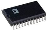
| 描述 | IC ADC 14BIT DUAL 500KSPS 24-TSS模数转换器 - ADC Bipolar Input Dual 14B 2Ch SAR |
| 产品分类 | |
| 品牌 | Analog Devices |
| 产品手册 | |
| 产品图片 |
|
| rohs | 符合RoHS无铅 / 符合限制有害物质指令(RoHS)规范要求 |
| 产品系列 | 数据转换器IC,模数转换器 - ADC,Analog Devices AD7367BRUZ-5- |
| 数据手册 | |
| 产品型号 | AD7367BRUZ-5 |
| 产品目录页面 | |
| 产品种类 | 模数转换器 - ADC |
| 位数 | 14 |
| 供应商器件封装 | 24-TSSOP |
| 信噪比 | 76 dB |
| 其它名称 | AD7367BRUZ5 |
| 分辨率 | 14 bit |
| 包装 | 管件 |
| 商标 | Analog Devices |
| 安装类型 | 表面贴装 |
| 安装风格 | SMD/SMT |
| 封装 | Tube |
| 封装/外壳 | 24-TSSOP(0.173",4.40mm 宽) |
| 封装/箱体 | TSSOP-24 |
| 工作温度 | -40°C ~ 85°C |
| 工作电源电压 | 5 V |
| 工厂包装数量 | 62 |
| 接口类型 | Serial (SPI, QSPI, Microwire) |
| 数据接口 | DSP,MICROWIRE™,QSPI™,串行,SPI™ |
| 最大功率耗散 | 54.5 mW |
| 最大工作温度 | + 85 C |
| 最小工作温度 | - 40 C |
| 标准包装 | 62 |
| 特性 | 同步采样 |
| 电压参考 | Internal, External |
| 电压源 | 模拟和数字,双 ± |
| 系列 | AD7367-5 |
| 结构 | SAR |
| 设计资源 | |
| 转换器数 | 2 |
| 转换器数量 | 2 |
| 转换速率 | 500 kS/s |
| 输入数和类型 | 4 个单端,单极4 个单端,双极 |
| 输入类型 | Differential |
| 通道数量 | 2 Channel |
| 采样率(每秒) | 500k |


- 商务部:美国ITC正式对集成电路等产品启动337调查
- 曝三星4nm工艺存在良率问题 高通将骁龙8 Gen1或转产台积电
- 太阳诱电将投资9.5亿元在常州建新厂生产MLCC 预计2023年完工
- 英特尔发布欧洲新工厂建设计划 深化IDM 2.0 战略
- 台积电先进制程称霸业界 有大客户加持明年业绩稳了
- 达到5530亿美元!SIA预计今年全球半导体销售额将创下新高
- 英特尔拟将自动驾驶子公司Mobileye上市 估值或超500亿美元
- 三星加码芯片和SET,合并消费电子和移动部门,撤换高东真等 CEO
- 三星电子宣布重大人事变动 还合并消费电子和移动部门
- 海关总署:前11个月进口集成电路产品价值2.52万亿元 增长14.8%


PDF Datasheet 数据手册内容提取
True Bipolar Input, 12-/14-Bit, 2-Channel, Simultaneous Sampling SAR ADCs AD7366-5/AD7367-5 FEATURES FUNCTIONAL BLOCK DIAGRAM Dual 12-bit/14-bit, 2-channel ADCs VDD DCAPA AVCC DVCC True bipolar analog inputs Programmable input ranges REF BUF ±10 V, ±5 V, 0 V to +10 V AD7366-5/AD7367-5 ±12 V with +3 V external reference Throughput rate: 500 kSPS VA1 12-/14-BIT Simultaneous conversion with read in less than 2 μs MUX T/H APSPURCOCXEISMSAITVIEON DORUITVPEURTS DOUTA High analog input impedance ADC Low current consumption VA2 SCLK 5.1 mA typical in normal mode CNVST CS 320 nA typical in shutdown mode CONTROL BUSY AD7366-5 LOGIC ADDR RANGE0 72 dB SNR at 50 kHz input frequency RANGE1 12-bit no missing codes REFSEL AD7367-5 VB1 VDRIVE 76 dB SNR at 50 kHz input frequency MUX T/H 12-/14-BIT 14-bit no missing codes SUCCESSIVE OUTPUT APPROXIMATION DRIVERS DOUTB Accurate on-chip reference: 2.5 V ± 0.2% ADC –40°C to +85°C operation VB2 BUF High speed serial interface iCMSPOIS-/ QprSoPcIe-/sMs ItCeRchOnWoIlRoEg-y/ DSP-compatible AGND AGND VSS DCAPB DGND 06842-001 Figure 1. Available in a 24-lead TSSOP GENERAL DESCRIPTION The devices have an on-chip 2.5 V reference that can be disabled to The AD7366-5/AD7367-51 are dual, 12-/14-bit, low power, allow the use of an external reference. If a 3 V reference is applied successive approximation analog-to-digital converters (ADCs) to the DCAPA and DCAPB pins, the AD7366-5/AD7367-5 can that feature throughput rates up to 500 kSPS. Each device contains accept a true bipolar ±12 V analog input. Minimum ±12 V VDD two ADCs, which are both preceded by a 2-channel multiplexer, and VSS supplies are required for the ±12 V input range. and a low noise, wide bandwidth, track-and-hold amplifier. PRODUCT HIGHLIGHTS The AD7366-5/AD7367-5 are fabricated on the Analog 1. True bipolar analog input signals can be accepted, as well Devices, Inc., industrial CMOS process (iCMOS®)2, which is as ±10 V, ±5 V, ±12 V (with external reference), and 0 V to a technology platform combining the advantages of low and +10 V unipolar signals. high voltage CMOS. The process allows the parts to accept 2. Two complete ADC functions allow simultaneous high voltage bipolar signals in addition to reducing power sampling and conversion of two channels. consumption and package size. The AD7366-5/AD7367-5 can accept true bipolar analog input signals in the ±10 V range, 3. A 500 kSPS serial interface is SPI-/QSPI™-/MICROWIRE™-/ ±5 V range, and 0 V to +10 V range. DSP-compatible. Table 1. Related Products Device Resolution Throughput Rate No. of Channels AD7366 12-Bit 1 MSPS Dual, 2-channel 1 Protected by U.S. Patent No. 6,731,232. 2 For analog systems designers within industrial/instrumentation equipment AD7366-5 12-Bit 500 kSPS Dual, 2-channel OEMs who need high performance ICs at higher voltage levels, iCMOS is a AD7367 14-Bit 1 MSPS Dual, 2-channel technology platform that enables the development of analog ICs capable of AD7367-5 14-Bit 500 kSPS Dual, 2-channel +30 V and operating at ±15 V supplies while allowing dramatic reductions in power consumption and package size, and increased ac and dc performance. Rev. B Information furnished by Analog Devices is believed to be accurate and reliable. However, no responsibility is assumed by Analog Devices for its use, nor for any infringements of patents or other One Technology Way, P.O. Box 9106, Norwood, MA 02062-9106, U.S.A. rights of third parties that may result from its use. Specifications subject to change without notice. No license is granted by implication or otherwise under any patent or patent rights of Analog Devices. Tel: 781.329.4700 www.analog.com Trademarks and registered trademarks are the property of their respective owners. Fax: 781.461.3113 ©2007-2011 Analog Devices, Inc. All rights reserved.
AD7366-5/AD7367-5 TABLE OF CONTENTS Features..............................................................................................1 Typical Connection Diagram...................................................18 Functional Block Diagram..............................................................1 Driver Amplifier Choice...........................................................19 General Description.........................................................................1 Reference.....................................................................................19 Product Highlights...........................................................................1 Modes of Operation.......................................................................20 Revision History...............................................................................2 Normal Mode..............................................................................20 Specifications.....................................................................................3 Shutdown Mode.........................................................................21 AD7366-5 Specifications.............................................................3 Power-Up Times.........................................................................21 AD7367-5 Specifications.............................................................5 Serial Interface................................................................................22 Timing Specifications..................................................................7 Microprocessor Interfacing...........................................................24 Absolute Maximum Ratings............................................................8 AD7366-5/AD7367-5 to ADSP-218x......................................24 ESD Caution..................................................................................8 AD7366-5/AD7367-5 to ADSP-BF53x...................................25 Pin Configuration and Function Descriptions.............................9 AD7366-5/AD7367-5 to TMS320VC5506.............................25 Typical Performance Characteristics...........................................11 AD7366-5/AD7367-5 to DSP563xx.........................................26 Terminology....................................................................................14 Application Hints...........................................................................27 Theory of Operation......................................................................16 Layout and Grounding..............................................................27 Circuit Information....................................................................16 Evaluating the AD7366-5/AD7367-5......................................27 Converter Operation..................................................................16 Outline Dimensions.......................................................................28 Analog Inputs..............................................................................17 Ordering Guide..........................................................................28 Transfer Function.......................................................................17 REVISION HISTORY 7/11—Rev. A to Rev. B Changes to Serial Interface Section..............................................22 Changes to Figure 27......................................................................23 8/09—Rev. 0 to Rev. A Changes to Table 2............................................................................4 Changes to Table 3............................................................................6 7/07—Revision 0: Initial Version Rev. B | Page 2 of 28
AD7366-5/AD7367-5 SPECIFICATIONS AD7366-5 SPECIFICATIONS AV = DV = 4.75 V to 5.25 V; V = 5 V to 16.5 V; V = −16.5 V to −5 V; V = 2.7 V to 5.25 V; f = 500 kSPS; f = 20 MHz; CC CC DD SS DRIVE SAMPLE SCLK V = 2.5 V internal/external; T = −40°C to +85°C, unless otherwise noted. REF A Table 2. Parameter Min Typ Max Unit Test Conditions/Comments DYNAMIC PERFORMANCE f = 50 kHz sine wave IN Signal-to-Noise Ratio (SNR)1 70 72 dB Signal-to-Noise (+ Distortion) Ratio (SINAD)1 70 71 dB Total Harmonic Distortion (THD)1 −85 −78 dB Spurious-Free Dynamic Range (SFDR)1 −87 −78 dB Intermodulation Distortion (IMD)1 fa = 49 kHz, fb = 51 kHz Second-Order Terms −88 dB Third-Order Terms −88 dB Channel-to-Channel Isolation1 −90 dB SAMPLE AND HOLD Aperture Delay2 10 ns Aperture Jitter2 40 ps Aperture Delay Matching2 ±100 ps Full Power Bandwidth 35 MHz @ 3 dB, ±10 V range 8 MHz @ 0.1 dB, ±10 V range DC ACCURACY Resolution 12 Bits Integral Nonlinearity (INL)1 ±0.5 ±1 LSB Differential Nonlinearity (DNL)1 ±0.25 ±0.5 LSB Guaranteed no missed codes to 12 bits Positive Full-Scale Error1 ±1 ±7 LSB ±5 V and ±10 V analog input range ±1 ±6 LSB 0 V to 10 V analog input range Positive Full-Scale Error Match1 ±1.5 LSB Matching from ADC A to ADC B ±0.1 LSB Channel-to-channel matching for ADC A and ADC B Zero Code Error1 ±0.5 ±3 LSB ±5 V and ±10 V analog input range ±1 ±6 LSB 0 V to 10 V analog input range Zero Code Error Match1 ±1.5 LSB Matching from ADC A to ADC B ±0.1 LSB Channel-to-channel matching for ADC A and ADC B Negative Full-Scale Error1 ±1 ±7 LSB ±5 V and ±10 V analog input range ±1 ±6 LSB 0 V to 10 V analog input range Negative Full-Scale Error Match1 ±1.5 LSB Matching from ADC A to ADC B ±0.1 LSB Channel-to-channel matching for ADC A and ADC B ANALOG INPUT Input Voltage Ranges ±10 V (Programmed via RANGE Pins) ±5 V 0 to 10 V DC Leakage Current ±0.01 ±1 μA Input Capacitance 9 pF When in track, ±10 V range 13 pF When in track, ±5 V or 0 V to +10 V range Input Impedance 500 kΩ For ±10 V @ 500 kSPS 2.5 MΩ For ±10 V @ 100 kSPS 250 kΩ For ±5 V/0 V to +10 V @ 500 kSPS 1.2 MΩ For ±5 V/0 V to +10 V @ 100 kSPS Rev. B | Page 3 of 28
AD7366-5/AD7367-5 Parameter Min Typ Max Unit Test Conditions/Comments REFERENCE INPUT/OUTPUT Reference Output Voltage3 2.494 2.5 2.506 V ±0.2% maximum @ 25°C Long-Term Stability 150 ppm For 1000 hours Output Voltage Hysteresis1 50 ppm Reference Input Voltage Range 2.5 3.0 V DC Leakage Current ±0.01 ±1 μA External reference applied to Pin D A/Pin D B CAP CAP Input Capacitance 25 pF ±5 V and ±10 V analog input range 17 pF 0 V to 10 V analog input range D A, D B Output Impedance 7 Ω CAP CAP Reference Temperature Coefficient 6 25 ppm/°C V Noise 20 μV rms Bandwidth = 3 kHz REF LOGIC INPUTS Input High Voltage, V 0.7 × V V INH DRIVE Input Low Voltage, V +0.8 V INL Input Current, I ±0.01 ±1 μA V = 0 V or V IN IN DRIVE Input Capacitance, C 2 6 pF IN LOGIC OUTPUTS Output High Voltage, V V − 0.2 V OH DRIVE Output Low Voltage, V 0.4 V OL Floating State Leakage Current ±0.01 ±1 μA Floating State Output Capacitance2 8 pF CONVERSION RATE Conversion Time 1.25 μs Track/Hold Acquisition Time2 140 ns Full-scale step input Throughput Rate 500 kSPS For 2.7 V ≤ V ≤ 5.25 V, f = 20 MHz DRIVE SCLK POWER REQUIREMENTS Digital inputs = 0 V or V DRIVE V 4.75 5.25 V See Table 7 CC V 5 16.5 V See Table 7 DD V −16.5 −5 V See Table 7 SS V 2.7 5.25 V DRIVE Normal Mode (Static) I 370 550 μA V = 16.5 V DD DD I 40 60 μA V = −16.5 V SS SS I 1.5 2.25 mA V = 5.5 V CC CC Normal Mode (Operational) f = 500 kSPS S I 1 1.2 mA V = 16.5 V DD DD I 0.7 0.82 mA V = −16.5 V SS SS I 3.4 4 mA V = 5.25 V, internal reference enabled CC CC Shutdown Mode I 0.01 1 μA V = 16.5 V DD DD I 0.01 1 μA V = −16.5 V SS SS I 0.3 3 μA V = 5.25 V CC CC Power Dissipation Normal Mode (Operational) 46 54.5 mW V = +16.5 V, V = −16.5 V, V = +5.25 V, DD SS CC f = 500 kSPS S 15 mW ±10 V input range, f = 100 kSPS S 20 mW ±5 V and 0 V to +10 V input range, f = 100 kSPS S Shutdown Mode 1.9 48.75 μW V = +16.5 V, V = −16.5 V, V = +5.25 V DD SS CC 1 See the Terminology section. 2 Sample tested during initial release to ensure compliance. 3 Refers to Pin DCAPA or Pin DCAPB specified for 25oC. Rev. B | Page 4 of 28
AD7366-5/AD7367-5 AD7367-5 SPECIFICATIONS AV = DV = 4.75 V to 5.25 V; V = 5 V to 16.5 V; V = −16.5 V to −5 V; V = 2.7 V to 5.25 V; f = 500 kSPS; f = 20 MHz; CC CC DD SS DRIVE SAMPLE SCLK V = 2.5 V internal/external; T = −40°C to +85°C, unless otherwise noted. REF A Table 3. Parameter Min Typ Max Unit Test Conditions/Comments DYNAMIC PERFORMANCE f = 50 kHz sine wave IN Signal-to-Noise Ratio (SNR)1 74 76 dB Signal-to-Noise (+ Distortion) Ratio (SINAD)1 73 75 dB Total Harmonic Distortion (THD)1 −84 −78 dB Spurious-Free Dynamic Range (SFDR)1 −87 −79 dB Intermodulation Distortion (IMD)1 fa = 49 kHz, fb = 51 kHz Second-Order Terms −91 dB Third-Order Terms −89 dB Channel-to-Channel Isolation1 −90 dB SAMPLE AND HOLD Aperture Delay2 10 ns Aperture Jitter2 40 ps Aperture Delay Matching2 ±100 ps Full Power Bandwidth 35 MHz @ 3 dB, ±10 V range 8 MHz @ 0.1 dB, ±10 V range DC ACCURACY Resolution 14 Bits Integral Nonlinearity (INL)1 ±2 ±3.5 LSB Differential Nonlinearity (DNL)1 ±0.5 ±0.90 LSB Guaranteed no missed codes to 14 bits Positive Full-Scale Error1 ±4 ±25 LSB ±5 V and ±10 V analog input range ±5 ±25 LSB 0 V to 10 V analog input range Positive Full-Scale Error Match1 ±3 LSB Matching from ADC A to ADC B ±0.2 LSB Channel-to-channel matching for ADC A and ADC B Zero Code Error1 ±1 ±10 LSB ±5 V and ±10 V analog input range ±5 ±25 LSB 0 V to 10 V analog input range Zero Code Error Match1 ±3 LSB Matching from ADC A to ADC B ±0.2 LSB Channel-to-channel matching for ADC A and ADC B Negative Full-Scale Error1 ±4 ±25 LSB ±5 V and ±10 V analog input range ±5 ±25 LSB 0 V to 10 V analog input range Negative Full-Scale Error Match1 ±3 LSB Matching from ADC A to ADC B ±0.2 LSB Channel-to-channel matching for ADC A and ADC B ANALOG INPUT Input Voltage Ranges ±10 V (Programmed via RANGE Pins) ±5 V 0 to 10 V See Table 7 DC Leakage Current ±0.01 ±1 μA Input Capacitance 9 pF When in track, ±10 V range 13 pF When in track, ±5 V or 0 V to +10 V range Input Impedance 500 kΩ For ±10 V @ 500 kSPS 2.5 MΩ For ±10 V @ 100 kSPS 250 kΩ For ±5 V/0 V to +10 V @ 500 kSPS 1.2 MΩ For ±5 V/0 V to +10 V @ 100 kSPS Rev. B | Page 5 of 28
AD7366-5/AD7367-5 Parameter Min Typ Max Unit Test Conditions/Comments REFERENCE INPUT/OUTPUT Reference Output Voltage3 2.494 2.5 2.506 V ±0.2% maximum @ 25°C Long-Term Stability 150 ppm For 1000 hours Output Voltage Hysteresis1 50 ppm Reference Input Voltage Range 2.5 3.0 V DC Leakage Current ±0.01 ±1 μA External reference applied to D A/Pin D B CAP CAP Input Capacitance 25 pF ±5 V and ±10 V analog input range 17 pF 0 V to 10 V analog input range D A, D B Output Impedance 7 Ω CAP CAP Reference Temperature Coefficient 6 25 ppm/°C V Noise 20 μV rms Bandwidth = 3 kHz REF LOGIC INPUTS Input High Voltage, V 0.7 × V V INH DRIVE Input Low Voltage, V 0.8 V INL Input Current, I ±0.01 ±1 μA V = 0 V or V IN IN DRIVE Input Capacitance, C 2 6 pF IN LOGIC OUTPUTS Output High Voltage, V V − 0.2 V OH DRIVE Output Low Voltage, V 0.4 V OL Floating State Leakage Current ±0.01 ±1 μA Floating State Output Capacitance2 8 pF CONVERSION RATE Conversion Time 1.25 ns Track/Hold Acquisition Time2 140 ns Full-scale step input Throughput Rate 500 kSPS For 2.7 V ≤ V ≤ 5.25 V, f = 20 MHz DRIVE SCLK POWER REQUIREMENTS Digital inputs = 0 V or V DRIVE V 4.75 5.25 V See Table 7 CC V 5 16.5 V See Table 7 DD V −16.5 −5 V See Table 7 SS V 2.7 5.25 V DRIVE Normal Mode (Static) I 370 550 μA V = 16.5 V DD DD I 40 60 μA V = −16.5 V SS SS I 1.5 2.25 mA V = 5.5 V CC CC Normal Mode (Operational) f = 500 kSPS S I 1 1.2 mA V = 16.5 V DD DD I 0.7 0.82 mA V = −16.5 V SS SS I 3.4 4 mA V = 5.25 V, internal reference enabled CC CC Shutdown Mode I 0.01 1 μA V = 16.5 V DD DD I 0.01 1 μA V = −16.5 V SS SS I 0.3 3 μA V = 5.25 V CC CC Power Dissipation Normal Mode (Operational) 46 54.5 mW V = +16.5 V, V = −16.5 V, V = +5.25 V DD SS CC 15 mW ±10 V input range, f = 100 kSPS S 20 mW ±5 V and 0 V to +10 V input range, f = 100 kSPS S Shutdown Mode 1.9 48.75 μW V = +16.5 V, V = −16.5 V, V = +5.25 V DD SS CC 1 See the Terminology section. 2 Sample tested during initial release to ensure compliance. 3 Refers to Pin DCAPA or Pin DCAPB. Rev. B | Page 6 of 28
AD7366-5/AD7367-5 TIMING SPECIFICATIONS AV = DV = 4.75 V to 5.25 V; V = 5 V to 16.5 V; V = −16.5 V to −5 V; V = 2.7 V to 5.25 V; T = T to T , unless otherwise noted.1 CC CC DD SS DRIVE A MIN MAX Table 4. Parameter 2.7 V ≤ V ≤ 5.25 V Unit Test Conditions/Comments DRIVE t Conversion time, internal clock. CONVST falling edge to BUSY falling edge. CONVERT 1.25 μs max For the AD7367-5. 1.25 μs max For the AD7366-5. f 10 kHz min Frequency of serial read clock. SCLK 20 MHz max t 50 ns min Minimum quiet time required between the end of serial read and the start of the next QUIET conversion. t 10 ns min Minimum CONVST low pulse. 1 t 40 ns min CONVST falling edge to BUSY rising edge. 2 t 0 ns min BUSY falling edge to MSB valid once CS is low for t prior to BUSY going low. 3 4 t 10 ns max Delay from CS falling edge until Pin 1 (D A) and Pin 23 (D B) are three-state disabled. 4 OUT OUT t 2 20 ns max Data access time after SCLK falling edge. 5 t 7 ns min SCLK to data valid hold time. 6 t 0.3 × t ns min SCLK low pulse width. 7 SCLK t 0.3 × t ns min SCLK high pulse width. 8 SCLK t 10 ns max CS rising edge to D A, D B, high impedance. 9 OUT OUT t 70 μs max Power up time from shutdown mode; time required between CONVST rising edge and POWER-UP CONVST falling edge. 1 Sample tested during initial release to ensure compliance. All input signals are specified with tR = tF = 5 ns (10% to 90% of VDRIVE) and timed from a voltage level of 1.6 V. All timing specifications given are with a 25 pF load capacitance. With a load capacitance greater than this value, a digital buffer or latch must be used. See the Terminology section and Figure 25. 2 The time required for the output to cross is 0.4 V or 2.4 V. Rev. B | Page 7 of 28
AD7366-5/AD7367-5 ABSOLUTE MAXIMUM RATINGS Stresses above those listed under Absolute Maximum Ratings Table 5. may cause permanent damage to the device. This is a stress Parameter Rating rating only; functional operation of the device at these or any V to AGND, DGND −0.3 V to +16.5 V DD other conditions above those indicated in the operational V to AGND, DGND −16.5 V to +0.3 V SS section of this specification is not implied. Exposure to absolute V to DGND −0.3 V to DV DRIVE CC maximum rating conditions for extended periods may affect V to AV (V − 0.3 V) to +16.5 V DD CC CC device reliability. AV to AGND, DGND −0.3 V to +7 V CC DVCC to AVCC −0.3 V to +0.3 V DV to DGND −0.3 V to +7 V CC ESD CAUTION V to AGND −0.3 V to DV DRIVE CC AGND to DGND −0.3 V to +0.3 V Analog Input Voltage to AGND V − 0.3 V to V + 0.3 V SS DD Digital Input Voltage to DGND −0.3 V to V + 0.3 V DRIVE Digital Output Voltage to GND −0.3 V to V + 0.3 V DRIVE D B, D B Input to AGND −0.3 V to AV + 0.3 V CAP CAP CC Input Current to Any Pin Except Supplies1 ±10 mA Operating Temperature Range −40°C to +85°C Storage Temperature Range −65°C to +150°C Junction Temperature 150°C TSSOP Package θ Thermal Impedance 128°C/W JA θ Thermal Impedance 42°C/W JC Pb-free Temperature, Soldering Reflow 260(+0)°C ESD 1.5 kV 1 Transient currents of up to 100 mA do not cause latch-up. Rev. B | Page 8 of 28
AD7366-5/AD7367-5 PIN CONFIGURATION AND FUNCTION DESCRIPTIONS DOUTA 1 24 DGND VDRIVE 2 23 DOUTB DVCC 3 22 BUSY RANGE1 4 AD7366-5/ 21 CNVST AD7367-5 RANGE0 5 20 SCLK ADDR 6 (NToOt Pto V SIEcWale) 19 CS AGND 7 18 REFSEL AVCC 8 17 AGND DCAPA 9 16 DCAPB VSS 10 15 VDD VVAA12 1112 1143 VVBB12 06842-002 Figure 2. Pin Configuration Table 6. Pin Function Descriptions Pin No. Mnemonic Description 1, 23 D A, D B Serial Data Outputs. The data output is supplied to each pin as a serial data stream. The bits are clocked out on OUT OUT the falling edge of the SCLK input and 12 SCLK cycles are required to access the data from the AD7366-5 while 14 SCLK cycle are required for the AD7367-5. The data simultaneously appears on both pins from the simultaneous conversions of both ADCs. The data stream consists of the 12 bits of conversion data for the AD7366-5 and 14 bits for the AD7367-5 and is provided MSB first. If CS is held low for a further 12 SCLK cycles for the AD7366-5 or 14 SCLK cycles for the AD7367-5, on either D A or D B, the data from the other ADC follows on that D pin. This OUT OUT OUT allows data from a simultaneous conversion on both ADCs to be gathered in serial format on either D A or OUT D B using only one serial port. See the Serial Interface section for more information. OUT 2 V Logic Power Supply Input. The voltage supplied at this pin determines at what voltage the interface operates. DRIVE This pin should be decoupled to DGND. The voltage range on this pin is 2.7 V to 5.25 V and may be different than the voltage at AV and DV , but should never exceed either by more than 0.3 V. CC CC 3 DV Digital Supply Voltage, 4.75 V to 5.25 V. The DV and AV voltages should ideally be at the same potential. CC CC CC For best performance, it is recommended that the DV and AV pins be shorted together, to ensure that the CC CC voltage difference between them never exceeds 0.3 V, even on a transient basis. This supply should be decoupled to DGND. Place 10 μF and 100 nF decoupling capacitors on the DV pin. CC 4, 5 RANGE1, Analog Input Range Selection, Logic Inputs. The polarity on these pins determines the input range of the analog RANGE0 input channels. See the Analog Inputs section and Table 8 for details. 6 ADDR Multiplexer Select, Logic Input. This input is used to select the pair of channels to be simultaneously converted, either Channel 1 of both ADC A and ADC B, or Channel 2 of both ADC A and ADC B. The logic state on this pin is latched on the rising edge of BUSY to set up the multiplexer for the next conversion. 7, 17 AGND Analog Ground. Ground reference point for all analog circuitry on the AD7366-5/AD7367-5. All analog input signals and any external reference signal should be referred to this AGND voltage. Both AGND pins should connect to the AGND plane of a system. The AGND and DGND voltages ideally should be at the same potential and must not be more than 0.3 V apart, even on a transient basis. 8 AV Analog Supply Voltage, 4.75 V to 5.25 V. This is the supply voltage for the ADC cores. The AV and DV voltages CC CC CC should ideally be at the same potential. For best performance, it is recommended that the DV and AV pins be CC CC shorted together to ensure that the voltage difference between them never exceeds 0.3 V even on a transient basis. This supply should be decoupled to AGND. Place 10 μF and 100 nF decoupling capacitors on the AV pin. CC 9, 16 D A, D B Decoupling Capacitor Pins. Decoupling capacitors are connected to these pins to decouple the reference buffer CAP CAP for each respective ADC. For best performance, it is recommended to use a 680 nF decoupling capacitor on these pins. Provided the output is buffered, the on-chip reference can be taken from these pins and applied externally to the rest of a system. 10 V Negative Power Supply Voltage. This is the negative supply voltage for the high voltage analog input structure SS of the AD7366-5/AD7367-5. The supply must be less than or equal to −5 V (see Table 7 for further details). Place 10 μF and 100 nF decoupling capacitors on the V pin. SS 11, 12 V , V Analog Inputs of ADC A. These are both single-ended analog inputs. The analog input range on these channels is A1 A2 determined by the RANGE0 and RANGE1 pins. 13, 14 V , V Analog Inputs of ADC B. These are both single-ended analog inputs. The analog input range on these channels is B2 B1 determined by the RANGE0 and RANGE1 pins. 15 V Positive Power Supply Voltage. This is the positive supply voltage for the high voltage analog input structure DD of the AD7366-5/AD7367-5. The supply must be greater than or equal to 5 V (see Table 7 for further details). Place 10 μF and 100 nF decoupling capacitors on the V pin. DD Rev. B | Page 9 of 28
AD7366-5/AD7367-5 Pin No. Mnemonic Description 18 REFSEL Internal/External Reference Selection, Logic Input. If this pin is tied to logic high, the on-chip 2.5 V reference is used as the reference source for both ADC A and ADC B. In addition, Pin D A and Pin D B must be tied to CAP CAP decoupling capacitors. If the REFSEL pin is tied to GND, an external reference can be supplied to the AD7366-5/ AD7367-5 through the D A and/or D B pins. CAP CAP 19 CS Chip Select, Active Low Logic Input. This input frames the serial data transfer. When CS is logic low, the output bus is enabled, and the conversion result is output on D A and D B. OUT OUT 20 SCLK Serial Clock, Logic Input. A serial clock input provides the SCLK for accessing the data from the AD7366-5/AD7367-5. 21 CNVST Conversion Start, Logic Input. This pin is edge triggered. On the falling edge of this input, the track/hold goes into hold mode and the conversion is initiated. If CNVST is low at the end of a conversion, the part goes into power- down mode. In this case, the rising edge of CNVST instructs the part to power up again. 22 BUSY Busy Output. BUSY transitions high when a conversion starts and remains high until the conversion completes. 24 DGND Digital Ground. This is the ground reference point for all digital circuitry on the AD7366-5/AD7367-5. The DGND pin should connect to the DGND plane of a system. The DGND and AGND voltages should ideally be at the same potential and must not be more than 0.3 V apart, even on a transient basis. Rev. B | Page 10 of 28
AD7366-5/AD7367-5 TYPICAL PERFORMANCE CHARACTERISTICS T = 25°C, unless otherwise noted. A 1.0 0.8 –76 0V TO +10V RANGE 0.6 –78 0.4 B) S ROR (L 0.02 D (dB) –80 ±5V RA±N1G0EV RANGE R H NL E –0.2 T –82 D –0.4 ––00..86 VADVDC C= =15 5VfVS,V , V =DDTS RV5SAI0CV =0=CE k –2==S15 P553°SCVVV –84 VADVDC C= =15 5VfVS,V , V =DDS RV5SI0CV =0CE k –==S1 P553SVVV INTERNAL REFERENCE INTERNAL REFERENCE –1.0 –86 0 2000 4000 6000 8C0O0D0E10000 12000 14000 16000 06842-003 10 ANALOG INPUT1 F0R0EQUENCY (kHz) 1000 06842-006 Figure 3. AD7367-5 Typical DNL Figure 6. THD vs. Analog Input Frequency 2.0 –66 AVCC = 5V, DVCC = 5V VDD = 15V, VSS = –15V 1.5 VfSD =R IV5E00 =k S3VPS RIN = 2000Ω INTERNAL REFERENCE 1.0 –71 ±5V RANGE B) S 0.5 L ERROR (L –0.50 THD (dB) –76 RIN = 5R1I0N0 =Ω 3000Ω RIN =R 4I7N0 =Ω 1300Ω N I –1.0 AVCC = 5V, DVCC = 5V –81 VDD = 15V, VSS = –15V VDRIVE = 3V RIN = 240Ω –1.5 fS = 500kSPS RIN = 56Ω TA = 25°C INTERNAL REFERENCE RIN = 3900Ω –2.00 2000 4000 6000 8C0O0D0E10000 12000 14000 16000 06842-004 –8610 ANALOG INPUT1 F0R0EQUENCY (kHz) 1000 06842-007 Figure 4. AD7367-5 Typical INL Figure 7. THD vs. Analog Input Frequency for Various Source Impedances 0 –20 VADVDC C= =15 5VV, ,V DSVSC =C –=1 55VV 77 VDRIVE = 3V fS = 500kSPS,fIN = 50kHz –40 INTERNAL REFERENCE 75 ±10V RANGE SNR = 76dB, SINAD = 75dB –60 dB) –80 D (dB) 73 0V TO +10V RANGE ( A N –100 SI 71 –120 AVCC = 5V, DVCC = 5V 69 VDD = 15V, VSS = –15V –140 VDRIVE = 3V fS = 500kSPS ±5V RANGE INTERNAL REFERENCE –160 67 0 50 FR10E0QUENCY (1k5H0z) 200 250 06842-005 10 ANALOG INPUT1 F0R0EQUENCY (kHz) 1000 06842-008 Figure 5. AD7367-5 FFT Figure 8. SINAD vs. Analog Input Frequency Rev. B | Page 11 of 28
AD7366-5/AD7367-5 –70 –70 B) –75 VCC, ADC A N (d –80 10N0mO VD Ep-CpO SUINPLEI NWGA VCEA POANC AITVOCRC OLATIO ––8850 ±5V RANGE VCC, ADC B VDD = 15VfS,V V=DS R5SI0V =0E k –=S1 P53SVV S –90 CHANNEL I ––9905 0V TO +10V RANGE PSRR (dB) –100 VDD, ADC B TO- ±10V RANGE VDD, ADC A VSS, ADC B NNEL- –100 VADVDC C= =15 5VV, ,V DSVSC =C –=1 55VV –110 CHA –105 fSV =D R5I0V0Ek =S P3SV VSS, ADC A INTERNAL REFERENCE –110 –120 0 100 FREQU20E0NCY OF3 I0N0PUT NO4IS00E (kHz)500 600 06842-009 0 200 SUPPL40Y0 RIPPLE6 F00REQUEN8C00Y (kHz)1000 1200 06842-011 Figure 9. Channel-to-Channel Isolation Figure 11. PSRR vs. Supply Ripple Frequency Without Supply Decoupling 110000 31 CODES 106091 CODES 344 CODES 40 AVCC = 5V, DVCC = 5V 100000 VDD = 15V, VSS = –15V VDRIVE = 3V VIN = 0V TO +10V 90000 fS = 500kSPS A) 30 INTERNAL REFERENCE 80000 T (µ 70000 EN 20 VIN = +5V R R 60000 CU VIN = +10V 50000 UT 10 P N 40000 OG I 0 30000 L A N 20000 A 10000 –10 VIN = –5V VIN = –10V 0 –20 8191 8192 8193CODE8194 8195 8196 06842-010 100 150 200THRO25U0GHPU3T00 RATE3 5(k0SPS)400 450 500 06842-012 Figure 10. Histogram of Codes for 200k Samples Figure 12. Analog Input Current vs. Throughput Rate Rev. B | Page 12 of 28
AD7366-5/AD7367-5 2.5050 45 AVCC = 5V, DVCC = 5V 2.5045 VDD = 15V, VSS = –15V 2.5040 40 VfSD =R IV5E00 =k S3VPS INTERNAL REFERENCE 2.5035 35 2.5030 W) 0V TO +10V RANGE ±5V RANGE V) m V (REF22..55002250 OWER ( 30 P 25 2.5015 2.5010 ±10V RANGE AVCC = 5V, DVCC = 5V 20 2.5005 VDD = 15V, VSS = –15V VDRIVE = 3V, 2.5000 15 0 10 20 30 CU4R0RENT5 (0µA) 60 70 80 90 06842-013 100 150 20S0AMPL2I5N0G FR3E0Q0UENC35Y0 (kSP4S0)0 450 500 06842-015 Figure 13. VREF vs. Reference Output Current Drive Figure 15. Power vs. Sampling Frequency in Normal Mode 0.300 0.250 DOUT SOURCE CURRENT V) (UT 0.200 O – V DOUT C 0.150 SINK CURRENT C V R O UT 0.100 O V 0.50 AVVDDCC = =1 55VV,, VDSVSC C= =1 55VV VDRIVE = 3V,fS = 500kSPS INTERNAL REFERENCE 0 0 500 10C0U0RRENT (1µ5A0)0 2000 2500 06842-014 Figure 14. DOUT Source Current vs. (VCC − VOUT ) and DOUT Sink Current vs. VOUT Rev. B | Page 13 of 28
AD7366-5/AD7367-5 TERMINOLOGY Differential Nonlinearity (DNL) Total Harmonic Distortion (THD) DNL is the difference between the measured and the ideal THD is the ratio of the rms sum of harmonics to the 1 LSB change between any two adjacent codes in the ADC. fundamental. For the AD7366-5/AD7367-5, it is defined as: Integral Nonlinearity (INL) V 2 +V 2 +V 2 +V 2 +V 2 THD(dB)=20log 2 3 4 5 6 INL is the maximum deviation from a straight line passing V 1 through the endpoints of the ADC transfer function. The where: endpoints of the transfer function are zero scale, a single (1) V is the rms amplitude of the fundamental. LSB point below the first code transition and full scale, a point 1 V, V, V, V, and V are the rms amplitudes of the second 1 LSB above the last code transition. 2 3 4 5 6 through the sixth harmonics. Zero Code Error Peak Harmonic or Spurious Noise This is the deviation of the midscale transition (all 1s to all 0s) Peak harmonic, or spurious noise, is defined as the ratio of the from the ideal V voltage, that is, AGND – ½ LSB for bipolar IN rms value of the next largest component in the ADC output ranges and 2 × V − 1 LSB for the unipolar range. REF spectrum (up to f/2, excluding dc) to the rms value of the S Positive Full-Scale Error fundamental. Normally, the value of this specification is deter- This is the deviation of the last code transition (011…110) to mined by the largest harmonic in the spectrum. However, for (011…111) from the ideal (that is, 4 × V − 1 LSB or 2 × V ADCs where the harmonics are buried in the noise floor, it is REF REF – 1 LSB) after the zero code error has been adjusted out. a noise peak. Negative Full-Scale Error Channel-to-Channel Isolation This is the deviation of the first code transition (10…000) to Channel-to-channel isolation is a measure of the level of cross- (10…001) from the ideal (that is, −4 × V + 1 LSB, −2 × V + talk between any two channels when operating in any of the REF REF 1 LSB, or AGND + 1 LSB) after the zero code error has been input ranges. It is measured by applying a full-scale, 150 kHz adjusted out. sine wave signal to all unselected input channels and determin- ing how much that signal is attenuated in the selected channel Zero Code Error Match with a 50 kHz signal. The figure given is the typical across all This is the difference in zero code error across all 12 channels. four channels for the AD7366-5/AD7367-5 (see the Figure 9 for more information). Positive Full-Scale Error Match This is the difference in positive full-scale error across all channels. Intermodulation Distortion With inputs consisting of sine waves at two frequencies, fa Negative Full-Scale Error Match and fb, any active device with nonlinearities creates distortion This is the difference in negative full-scale error across all channels. products at the sum, and different frequencies of mfa ± nfb Track-and-Hold Acquisition Time where m, n = 0, 1, 2, 3, and so on. Intermodulation distortion The track-and-hold amplifier returns to track mode at the end terms are those for which neither m nor n is equal to zero. of a conversion. Track-and-hold acquisition time is the time For example, the second-order terms include (fa + fb) and required for the output of the track-and-hold amplifier to reach (fa − fb), while the third-order terms include (2fa + fb), its final value, within ±½ LSB, after the end of conversion. (2fa − fb), (fa + 2fb), and (fa − 2fb). The AD7366-5/AD7367-5 is tested using the CCIF standard Signal-to-Noise (+ Distortion) Ratio (SINAD) where two input frequencies near the top end of the input This ratio is the measured ratio of signal-to-noise (+ distortion) bandwidth are used. In this case, the second-order terms are at the output of the ADC. The signal is the rms amplitude of the usually distanced in frequency from the original sine waves, fundamental. Noise is the sum of all nonfundamental signals up while the third-order terms are usually at a frequency close to to half the sampling frequency (f/2), excluding dc. The ratio is S the input frequencies. As a result, the second- and third-order dependent on the number of quantization levels in the digitiza- terms are specified separately. The calculation of the intermodula- tion process: the more levels, the smaller the quantization noise. tion distortion is as per the THD specification, where it is the ratio The theoretical signal-to-noise (+ distortion) ratio for an ideal of the rms sum of the individual distortion products to the rms N-bit converter with a sine wave input is given by: amplitude of the sum of the fundamentals expressed in decibels. Signal-to-Noise (+ Distortion) = (6.02N + 1.76) dB Thus, for a 12-bit converter, this is 74 dB. Rev. B | Page 14 of 28
AD7366-5/AD7367-5 Power Supply Rejection Ration (PSRR) It is expressed in ppm using the following equation: Variations in power supply affect the full-scale transition but V (25°C)−V (T_HYS) not the converter’s linearity. PSRR is the maximum change in V (ppm) = REF REF ×106 HYS V (25°C) the full-scale transition point due to a change in power supply REF voltage from the nominal value (see Figure 11). where: V (25°C) is V at 25°C. Thermal Hysteresis REF REF V (T_HYS) is the maximum change of V at T_HYS+ Thermal hysteresis is defined as the absolute maximum change REF REF or T_HYS−. of reference output voltage after the device is cycled through temperature from either T_HYS+ = +25°C to T to +25°C MAX or T_HYS− = +25°C to T to +25°C MIN Rev. B | Page 15 of 28
AD7366-5/AD7367-5 THEORY OF OPERATION CIRCUIT INFORMATION If the internal reference is the preferred option, the user must tie the REFSEL pin logic high. Alternatively, if REFSEL is tied to The AD7366-5/AD7367-5 are fast, dual, 2-channel, 12-/14-bit, GND, an external reference can be supplied to both ADCs bipolar input, simultaneous sampling, serial ADCs. The through the D A and D B pins. AD7366-5/AD7367-5 can accept bipolar input ranges of ±10 V CAP CAP and ±5 V. They can also accept a 0 V to 10 V unipolar input The analog inputs are configured as two single-ended inputs for range. The AD7366-5/AD7367-5 require V and V dual DD SS each ADC. The various different input voltage ranges can be supplies for the high voltage analog input structure. These selected by programming the RANGE bits as shown in Table 8. supplies must be greater than or equal to the analog input range (see Table 7 for the minimum requirements on these supplies CONVERTER OPERATION for each analog input range). The AD7366-5/AD7367-5 require The AD7366-5/AD7367-5 have two successive approximation a low voltage 4.75 V to 5.25 V V supply to power the ADC core. CC ADCs, each based around two capacitive DACs. Figure 16 and Figure 17 show simplified schematics of an ADC in acquisition Table 7. Reference and Supply Requirements for Each and conversion phases, respectively. The ADC is comprised of Analog Input Range control logic, a SAR, and a capacitive DAC. In Figure 16 (the Selected Full-Scale acquisition phase), SW2 is closed, SW1 is in Position A, the Analog Input Reference Input Minimum Range (V) Voltage (V) Range (V) AVCC (V) VDD/VSS (V) comparator is held in a balanced condition, and the sampling ±10 +2.5 ±10 +5 ±10 capacitor arrays acquire the signal on the input. +3.0 ±12 +5 ±12 ±5 +2.5 ±5 +5 ±5 CAPACITIVE DAC +3.0 ±6 +5 ±6 0 to +10 +2.5 0 to +10 +5 +10/AGND A +3.0 0 to +12 +5 +12/AGND VIN CONTROL SW1 B LOGIC Each AD7366-5/AD7367-5 contains two on-chip, track-and-hold SW2 ainmteprlfiafcieer ws,i tthw tow sou scecpeassriavtee dapatpar oouxtipmuatt pioinns .A TDhCe ds,e avnicde ais sheoruiasle d AGND COMPARATOR 06842-018 Figure 16. ADC Acquisition Phase in a 24-lead TSSOP, offering the user considerable space-saving advantages over alternative solutions. When the ADC starts a conversion (see Figure 17), SW2 opens, and SW1 moves to Position B, causing the comparator to The AD7366-5/AD7367-5 require a CNVST signal to start a become unbalanced. The control logic and the charge redis- conversion. On the falling edge of CNVST, both track-and- tribution DAC is used to add and subtract fixed amounts of holds are placed into hold mode, and the conversions are charge from the sampling capacitor to bring the comparator initiated. The BUSY signal goes high to indicate that the back into a balanced condition. When the comparator is conversions are taking place. The clock source for each balanced again, the conversion is complete. The control logic successive approximation ADC is provided by an internal generates the ADC output code. oscillator. The BUSY signal goes low to indicate the end of conversion. On the falling edge of BUSY, the track-and-hold CAPACITIVE returns to track mode. Once the conversion is finished, the DAC serial clock input accesses data from the part. A VIN CONTROL The AD7366-5/AD7367-5 have an on-chip 2.5 V reference that SW1 B LOGIC can be disabled when an external reference is preferred. If the SW2 ifnrotemrn DalC ArePAfe raenndc eD iCsA tPoB bme uusste fdir eslts bewe bhuerfefe irne da. sOysnt epmow, tehre- uopu,t tphuet AGND COMPARATOR 06842-019 Figure 17. ADC Conversion Phase REFSEL pin must be tied to a high or low logic state to select either the internal or external reference option. Rev. B | Page 16 of 28
AD7366-5/AD7367-5 ANALOG INPUTS TRANSFER FUNCTION Each ADC in the AD7366-5/AD7367-5 has two single-ended The output coding of the AD7366-5/AD7367-5 is twos comple- analog inputs. Figure 18 shows the equivalent circuit of the ment. The designed code transitions occur at successive integer analog input structure of the AD7366-5/AD7367-5. The two LSB values (that is, 1 LSB, 2 LSB, and so on). The LSB size is diodes provide ESD protection. Care must be taken to ensure dependent on the analog input range selected (see Table 10). that the analog input signals never exceed the supply rails by The ideal transfer characteristic is shown in Figure 19. more than 300 mV. Otherwise, these diodes become forward- Table 10. LSB Sizes for Each Analog Input Range biased and start conducting current into the substrate. The AD7366-5 AD7367-5 diodes can conduct up to 10 mA without causing irreversible Input Full-Scale LSB Size Full-Scale LSB Size damage to the part. The resistors are lumped components made Range Range (mV) Range (mV) up of the on resistance of the switches. The value of these resistors ±10 V 20 V/4096 4.88 20 V/16384 1.22 is typically 170 Ω. Capacitor C1 can primarily be attributed to ±5 V 10 V/4096 2.44 10 V/16384 0.61 pin capacitance while Capacitor C2 is the sampling capacitor of 0 V to +10 V 10 V/4096 2.44 10 V/16384 0.61 the ADC. The total lumped capacitance of C1 and C2 is approxi- mately 9 pF for the ±10 V input range and approximately 13 pF for all other input ranges. 011...111 011...110 VDD E VIN0 D R1 C2 C COD 001001001.........001001101 C1 D AD VSS 06842-020 110000......001001 Figure 18. Equivalent Analog Input Structure 100...000 TThhee aAnDal7o3g6 i6n-p5u/At Dca7n3 b6e7 -s5e tc taon ohnaen odfl et htrrueee rbaipnogelasr: ±in1p0u Vt ,v ±o5lt aVg,e osr. –FSR/2 + 1LASNBALO0GV INPU+TFSR/2 – 1LSB 06842-021 Figure 19. Transfer Characteristic 0 V to +10 V. The logic levels on Pin RANGE0 and Pin RANGE1 determine which input range is selected as outlined in Table 8. Track-and-Hold These range bits should not be changed during the acquisition The track-and-hold on the analog input of the AD7366-5/ time prior to a conversion, but can change at any other time. AD7367-5 allows the ADC to accurately convert an input sine Table 8. Analog Input Range Selection wave of full-scale amplitude to 12-/14-bit accuracy. The input RANGE0 RANGE1 Range Selected bandwidth of the track-and-hold is greater than the Nyquist 0 0 ±10 V rate of the ADC. The AD7366-5/AD7367-5 can handle frequencies up to 35 MHz. 1 0 ±5 V 0 1 0 V to +10 V The track-and-hold enters its tracking mode once the BUSY 1 1 Do not program signal goes low after the CS falling edge. The time required to The parts require VDD and VSS dual supplies for the high voltage acquire an input signal depends on how quickly the sampling analog input structures. These supplies must be greater than or capacitor is charged. With zero source impedance, 140 ns is equal to ±5 V (see Table 7 for the requirements on these supplies). sufficient to acquire the signal to the 12-bit level for the AD7366-5 The AD7366-5/AD7367-5 require a low voltage 4.75 V to 5.25 V and the 14-bit level for the AD7367-5. The acquisition time for AVCC supply to power the ADC core, a 4.75 V to 5.25 V DVCC the ±10 V, ±5 V, and 0 V to +10 V ranges to settle to within ±½ LSB supply for digital power, and a 2.7 V to 5.25 V VDRIVE supply for is typically 140 ns. The ADC goes back into hold mode on the interface power. falling edge of CNVST. Channel selection is made via the ADDR pin as shown in Table 9. The acquisition time required is calculated using the following The logic level on the ADDR pin is latched on the rising edge of formula: the BUSY signal for the next conversion, not the one in progress. t = 10 × ((R + R) × C) When power is first supplied to the AD7366-5/AD7367-5, the ACQ SOURCE default channel selection is VA1 and VB1. where: C is the sampling capacitance. Table 9. Channel Selection R is the resistance seen by the track-and-hold amplifier looking ADDR Channels Selected at the input. 0 V , V A1 B1 R should include any extra source impedance on the SOURCE 1 V , V A2 B2 analog input. Rev. B | Page 17 of 28
AD7366-5/AD7367-5 TYPICAL CONNECTION DIAGRAM Unlike other bipolar ADCs, the AD7366-5/AD7367-5 do not have a resistive analog input structure. On the AD7366-5/ Figure 20 shows a typical connection diagram for the AD7366-5/ AD7366-5, the bipolar analog signal is sampled directly onto AD7367-5. In this configuration, the AGND pin is connected the sampling capacitor. This gives the devices high analog input to the analog ground plane of the system, and the DGND pin impedance. The analog input impedance can be calculated from is connected to the digital ground plane of the system. The the following formula: analog inputs on the AD7366-5/AD7367-5 accept bipolar single-ended signals. The AD7366-5/AD7367-5 can operate Z = 1/(f × C) S S with either an internal or an external reference. In Figure 20, the where: AD7366-5/AD7367-5 is configured to operate with the internal fS is the sampling frequency. 2.5 V reference. A 680 nF decoupling capacitor is required when CS is the sampling capacitor value. operating with the internal reference. CS depends on the analog input range chosen (see the Analog The AVCC and DVCC pins are connected to a 5 V supply voltage. Inputs section). When operating at 500 kSPS, the analog input The V and V are the dual supplies for the high voltage analog DD SS impedance is typically 260 kΩ for the ±10 V range. As the input structures. The voltage on these pins must be greater than sampling frequency is reduced, the analog input impedance or equal to ±5 V (see Table 7 for more information). The V pin DRIVE further increases. As the analog input impedance increases, the is connected to the supply voltage of the microprocessor. The current required to drive the analog input therefore, decreases voltage applied to the V input controls the voltage of the DRIVE (see Figure 7 for more information). serial interface. V can be set to 3 V or 5 V. DRIVE + 0.1µF +5V SUPPLY +5V TO +16.5V SUPPLY + + + + 10µF 0.1µF 0.1µF 10µF VDD DVCC AVCC +3V OR +5V SUPPLY VA1 AD7366-5/VDRIVE 0.1µF + 10µF + AD7367-5 A±N5AVL, OANGD I N0PVU TTOS +±1100VV, VVVBBA122 CDDABSNOODUCVUUDCSLSTTRABKYST MICROCONTROLLER/MICROPROCESSOR DCAPA REFSEL VDRIVE SERIAL 680nF + DCAPB RANGE0 INTERFACE + RANGE1 680nF VSS AGND DGND –16.5V TO –5V SUPPLY +10µF +0.1µF 06842-022 Figure 20. Typical Connection Diagram for ±10 V Range Using Internal Reference Rev. B | Page 18 of 28
AD7366-5/AD7367-5 V DRIVER AMPLIFIER CHOICE DRIVE The AD7366-5/AD7367-5 also have a V feature to control Each AD7366-5/AD7367-5 has a total of four analog inputs, DRIVE the voltage at which the serial interface operates. V allows which operate in single-ended mode. Both ADC analog inputs DRIVE the ADC to easily interface to both 3 V and 5 V processors. For can be programmed to one of the three analog input ranges. In example, if the AD7366-5/AD7367-5 is operated with a V of applications where the signal source is high impedance, it is CC 5 V, the V pin could be powered from a 3 V supply, allowing recommended to buffer the signal before applying it to the DRIVE a large dynamic range with low voltage digital processors. Thus, ADC analog inputs. Figure 21 shows the configuration of the the AD7366-5/AD7367-5 could be used with the ±10 V input AD7366-5/AD7367-5 in single-ended mode. range while still being able to interface to 3 V digital parts. In applications where the THD and SNR are critical specifi- REFERENCE cations, the analog input of the AD7366-5/AD7367-5 should be driven from a low impedance source. Large source impedances The AD7366-5/AD7367-5 can operate with either the internal significantly affect the ac performance of the ADC and can 2.5 V on-chip reference or an externally applied reference. The necessitate the use of an input buffer amplifier. logic state of the REFSEL pin determines whether the internal reference is used. The internal reference is selected for both ADCs When no amplifier is used to drive the analog input, the source when the REFSEL pin is tied to logic high. If the REFSEL pin is impedance should be limited to low values. The maximum source tied to GND, an external reference can be supplied through the impedance depends on the amount of THD that can be tolerated D A and D B pins. On power-up, the REFSEL pin must be CAP CAP in the application. The THD increases as the source impedance tied to either a low logic or high logic state for the part to operate. increases and performance degrades. Figure 7 shows THD vs. Suitable reference sources for the AD7366-5/AD7367-5 include the analog input frequency for various source impedances. the AD780, AD1582, ADR431, REF193, and ADR391. Depending on the input range and analog input configuration selected, the AD7366-5/AD7367-5 can handle source The internal reference circuitry consists of a 2.5 V band gap impedances as illustrated in Figure 7. reference and a reference buffer. When operating the AD7366-5/ AD7367-5 in internal reference mode, the 2.5 V internal reference Due to the programmable nature of the analog inputs on the is available at the D A and D B pins, which should be CAP CAP AD7366-5/AD7367-5, the choice of op amp used to drive the decoupled to AGND using a 680 nF capacitor. It is recommended inputs is a function of the particular application and depends that the internal reference be buffered before applying it elsewhere on the selected analog input voltage ranges. in the system. The internal reference is capable of sourcing up to 150 μA with an analog input range of ±10 V and 70 μA for The driver amplifier must be able to settle for a full-scale step to both the ±5 V range and 0 V to +10 V range a 14-bit level, 0.0061%, in less than the specified acquisition time of the AD7366-5/AD7367-5. An op amp such as the AD8021 If the internal reference operation is required for the ADC meets this requirement when operating in single-ended mode. conversion, the REFSEL pin must be tied to logic high on power- The AD8021 needs an external compensating NPO type of up. The reference buffer requires 70 μs to power up and charge capacitor. The AD8022 can also be used in high frequency the 680 nF decoupling capacitor during the power-up time. applications where a dual version is required. For lower frequency applications, recommended op amps are the AD797, AD845, The AD7366-5/AD7367-5 is specified for a 2.5 V to 3 V reference and AD8610. range. When a 3 V reference is selected, the ranges are ±12 V, ±6 V, and 0 V to +12 V. For these ranges, the V and V supply DD SS V+ must be greater than or equal to the +12 V and −12 V, respectively. + 10µF +5V +10V/+5V + + 0.1µF AGND –10V/–5V AD8021 VA1 VDD DVCC/AVCC 1kΩ AD7366-5/ AD7367-5* 1kΩ 15pF + VSS 0.1µF + CCOMP= 10pF 10µF *ADDITIONAL PINSV–OMITTED FOR CLARITY. 06842-023 Figure 21. Typical Connection Diagram with the AD8021 Driving the Analog Input in Single-Ended Mode Rev. B | Page 19 of 28
AD7366-5/AD7367-5 MODES OF OPERATION The mode of operation for the AD7366-5/AD7367-5 is selected The BUSY signal remains high for the duration of the conversion. by the (logic) state of the CNVST signal at the end of a conver- The CS pin must be brought low to bring the data bus out of sion. There are two possible modes of operation: normal mode three-state; subsequently 12 SCLK cycles are required to read and shutdown mode. These modes of operation are designed to the conversion result from the AD7366-5, while 14 SCLK cycles provide flexible power management options, which can be are required to read from the AD7367-5. The D lines return OUT chosen to optimize the power dissipation/throughput rate to three-state only when CS is brought high. If CS is left low for ratio for differing application requirements. a further 12 SCLK cycles for the AD7366-5 or 14 SCLK cycles for the AD7367-5, the result from the other on-chip ADC is NORMAL MODE also accessed on the same D line, as shown in Figure 27 and OUT Normal mode is intended for applications needing fast Figure 28 (see the Serial Interface section). throughput rates because the user does not have to worry about any power-up times (with the AD7366-5/AD7367-5 After 24 SCLK cycles have elapsed for the AD7366-5 and 28 SCLK remaining fully powered at all times). Figure 22 shows the cycles have elapsed for the AD7367-5, the DOUT line returns to normal mode of operation for the AD7366-5, while Figure 23 three-state when CS is brought high (not on the 24th or 28th SCLK illustrates normal mode for the AD7367-5. falling edge). If CS is brought high prior to this, the DOUT line returns to three-state at that point. Thus, CS must be brought The conversion is initiated on the falling edge of CNVST as high once the read is completed because the bus does not described in the Circuit Information section. To ensure that automatically return to three-state upon completion of the the part remains fully powered up at all times, CNVST must be dual result read. at a logic high state prior to the BUSY signal going low. If CNVST is at a logic low state when the BUSY signal goes low, Once a data transfer is complete and DOUTA and DOUTB have the analog circuitry powers down and the part ceases converting. returned to three-state, another conversion can be initiated after the quiet time, t , has elapsed by bringing CNVST low again. QUIET t 1 CNVST t QUIET t 2 BUSY t CONVERT t 3 CS SCLK SERIAL READ OPERATION 1 12 06842-024 Figure 22. Normal Mode Operation for the AD7366-5 t 1 CNVST t QUIET t 2 BUSY t CONVERT t 3 CS SCLK SERIAL READ OPERATION 1 14 06842-025 Figure 23. Normal Mode Operation for the AD7367-5 Rev. B | Page 20 of 28
AD7366-5/AD7367-5 SHUTDOWN MODE POWER-UP TIMES Shutdown mode is intended for use in applications where slow As described in the Shutdown Mode section, the AD7366-5/ throughput rates are required. Shutdown mode is suited to AD7367-5 have one power-down mode. This section deals with applications where a series of conversions performed at a the power-up time required when coming out of this mode. It relatively high throughput rate are followed by a long period of should be noted that these power-up times apply with the inactivity and, thus, shutdown. When the AD7366-5/AD7367-5 recommended capacitors in place on the DCAPA and DCAPB pins. are in full power-down, all analog circuitry is powered down. To power up from shutdown, CNVST must be brought high and remain high for a minimum of 70 μs, as shown in Figure 24. The falling edge of CNVST initiates the conversion. The BUSY When power supplies are first applied to the AD7366-5/AD7367-5, output subsequently goes high to indicate that the conversion is in progress. Once the conversion is completed, the BUSY output the ADC can power up with CNVST in either the low or high returns low. If the CNVST signal is at logic low when BUSY logic state. Before attempting a valid conversion, CNVST must goes low, the part enters shutdown at the end of the conversion be brought high and remain high for the recommended power- phase. While the part is in shutdown mode, the digital output up time of 70 μs. CNVST can then be brought low to initiate a code from the last conversion on each ADC can still be read conversion. With the AD7366-5/AD7367-5, no dummy conversion from the DOUT pins. To read the DOUT data, CS must be brought is required before valid data can be read from the DOUT pins. low as described in the Serial Interface section. The D pins OUT If it is intended to place the part in shutdown mode when the return to three-state once CS is brought back to logic high. supplies are first applied, the AD7366-5/AD7367-5 must be powered up, and a conversion initiated. However, CNVST To exit full power-down and to power up the AD7366-5/ AD7367-5, a rising edge of CNVST is required. After the should remain in the logic low state, and when the BUSY signal goes low, the part enters shutdown. required power-up time has elapsed, CNVST may be brought low again to initiate another conversion, as shown in Figure 24 Once supplies are applied to the AD7366-5/AD7367-5, sufficient time must be allowed for any external reference to power up and to charge the various reference buffer decoupling capacitors to their final values. t ENTERS SHUTDOWN POWER-UP CNVST BUSY t2 t CONVERT t CS 3 SCLK 1 12 SERIAL READ OPERATION 06842-026 Figure 24. Autoshutdown Mode for AD7366-5 Rev. B | Page 21 of 28
AD7366-5/AD7367-5 SERIAL INTERFACE Figure 25 and Figure 26 show the detailed timing diagram for On the rising edge of CS, the conversion is terminated, and serial interfacing to the AD7366-5 and the AD7367-5. On the D and D return to three-state. If CS is not brought high OUTA OUTB falling edge of CNVST, the AD7366-5/AD7367-5 simultaneously but is instead held low for an additional 14 SCLK cycles, the convert the selected channels. These conversions are performed data from the other D pin follows on the selected D pin. OUT OUT using the on-chip oscillator. After the falling edge of CNVST, Note that the second serial result from the AD7366-5 is the BUSY signal goes high, indicating that the conversion has preceded by two zeros. See Figure 27 and Figure 28, where started. The BUSY signal returns low when the conversion has D is shown. In this case, the D line in use returns to OUTA OUT been completed. The data can now be read from the D pins. three-state on the rising edge of CS. OUT The CS and SCLK signals are required to transfer data from the If the falling edge of SCLK coincides with the falling edge of CS, AD7366-5/AD7367-5. The AD7366-5/AD7367-5 have two the falling edge of SCLK is not acknowledged by the AD7366-5/ output pins corresponding to each ADC. Data can be read from AD7367-5, and the next falling edge of SCLK is the first registered the AD7366-5/ AD7367-5 using both DOUTA and DOUTB. after the falling edges of the CS. Alternatively, a single output pin of the user’s choice can be used. The SCLK input signal provides the clock source for the serial The CS pin can be brought low before the BUSY signal goes low, interface. The CS goes low to access data from the AD7366- indicating the end of a conversion. When CS is at a logic low state, 5/AD7367-5. The falling edge of CS takes the bus out of three- the data bus is brought out of three-state. This feature can be state and clocks out the MSB of the conversion result. The data used to ensure that the MSB is valid on the falling edge of BUSY stream consists of 12 bits of data for the AD7366-5 and 14 bits of by bringing CS low a minimum of t4 before the BUSY signal data for the AD7367-5, MSB first. The first bit of the conversion goes low. The dotted CS line in Figure 22 and Figure 23 result is valid on the first SCLK falling edge after the CS falling illustrates this feature. edge. The subsequent 11-bits/ 13-bits of data for the AD7366- Alternatively, the CS pin can be tied to a low logic state continu- 5/AD7367-5, respectively, are clocked out on the falling edge of ously. In this case, the D pins never enter three-state, and the the SCLK signal. A minimum of 12 clock pulses must be OUT data bus is continuously active. Under these conditions, the MSB provided to the AD7366-5 to access each conversion result, and of the conversion result for the AD7366-5/AD7367-5 is available a minimum of 14 clock pulses must be provided to the AD7367- on the falling edge of the BUSY signal. The next most significant 5 to access the conversion result. Figure 25 shows how a 12 bit is available on the first SCLK falling edge after the BUSY SCLK read is used to access the conversion results for the signal has gone low. This mode of operation enables the user to AD7366-5, and Figure 26 illustrates the case for the AD7367-5 read the MSB as soon as it is made available by the converter. with a 14 SCLK read. CS t 8 SCLK 1 2 3 4 5 12 DDOOUUTTBA TSHTARTEEE- DB11t4DB10 DB9 DB8 t5 t6 Dt7B2 DB1 DBt90 THREE-STATE 06842-027 Figure 25. Serial Interface Timing Diagram for the AD7366-5 CS t 8 SCLK 1 2 3 4 5 14 DDOOUUTTBA TSHTARTEEE- DB13t4DB12 DB11 DB10 t5 t6 Dt7B2 DB1 DBt90 THREE-STATE 06842-028 Figure 26. Serial Interface Timing Diagram for the AD7367-5 Rev. B | Page 22 of 28
AD7366-5/AD7367-5 CS t 8 SCLK 1 2 3 4 5 10 11 12 13 14 26 t 7 t t t 4 5 6 DOUTATSHTARTEEE-DB11ADB10A DB9A DB1A DB0A 0 0 DB11B DB1B DB0B TSHTARTEEE- 06842-030 Figure 27. Reading Data from Both ADCs on One DOUT Line with 24 SCLKs for the AD7366-5 CS t 8 SCLK 1 2 3 4 5 12 13 14 15 28 t 7 t t t 3 5 6 DOUTATSHTARTEEE-DB13ADB12A DB11A DB1A DB0A DB13B DB12B DB1B DB0B TSHTARTEEE- 06842-029 Figure 28. Reading Data from Both ADCs on One DOUT Line with 28 SCLKs for the AD7367-5 Rev. B | Page 23 of 28
AD7366-5/AD7367-5 MICROPROCESSOR INTERFACING The serial interface on the AD7366-5/AD7367-5 allows the Table 11. SPORT0 Control Register Setup parts to be directly connected to a range of different micro- Setting Description processors. This section explains how to interface the AD7366-5/ TFSW = RFSW = 1 Alternate framing. AD7367-5 with some more common microcontrollers and DSP INVRFS = INVTFS = 1 Active low frame signal. serial interface protocols. DTYPE = 00 Right justify data. AD7366-5/AD7367-5 TO ADSP-218x SLEN = 1111 16-bit data-word (or can be set to 1101 for 14-bit data-word). The ADSP-218x family of DSPs interfaces directly to the ISCLK = 1 Internal serial clock. AD7366-5/AD7367-5 with no glue logic required. The V DRIVE TFSR = RFSR = 1 Frame every word. pin of the AD7366-5/AD7367-5 takes the same supply voltage IRFS = 0 as that of the ADSP-218x. This allows the ADC to operate at a ITFS = 1 higher supply voltage than its serial interface and therefore, the ADSP-218x, if necessary. The connection diagram in Figure 29 Table 12. SPORT1 Control Register Setup shows both DOUTA and DOUTB of the AD7366-5/AD7367-5 Setting Description connected to both serial ports of the ADSP-218x. The SPORT0 TFSW = RFSW = 1 Alternate framing. and SPORT1 control registers should be set up as shown in INVRFS = INVTFS = 1 Active low frame signal. Table 11 and Table 12. DTYPE = 00 Right justify data. SLEN = 1111 16-bit data-word (or can be set to 1101 AD7366-5/ ADSP-218x* for 14-bit data-word). AD7367-5* SCLK SCLK0 ISCLK = 0 External serial clock. SCLK1 TFSR = RFSR = 1 Frame every word. CS TFS0 IRFS = 0 RFS0 ITFS = 1 RFS1 The ADSP-218x has the TFS0 and RFS0 of the SPORT0 and the DOUTA DR0 RFS1 of SPORT1 tied together. TFS0 is set as an output, and both DOUTB DR1 RFS0 and RFS1 are set as inputs. The DSP operates in alternate BUSY IRQn framing mode, and the SPORT control registers are set up as CNVST FLn described in Table 11 and Table 12. The frame synchronization VDRIVE signal generated on the TFS0 is tied to CS. *ADDITIONAL PINS OMITTED FOR CLARITY. VDD 06842-031 Tthhee A ADDS7P3-26168-x5 /wAhDen7 3th67e -c5o nBvUeSrsYio lnin ies cpormovpildeetes. aTnh ien ctoernrvueprsti oton Figure 29. Interfacing the AD7366-5/AD7367-5 to the ADSP-218x results can then be read from the AD7366-5/AD7367-5 using a read operation. When an interrupt is received on IRQn from the BUSY signal, a value is transmitted with TFS/DT (ADC control word). The TFS is used to control the RFS and, therefore, the reading of data. Rev. B | Page 24 of 28
AD7366-5/AD7367-5 AD7366-5/AD7367-5 TO ADSP-BF53x AD7366-5/AD7367-5 TO TMS320VC5506 The ADSP-BF53x family of DSPs interfaces directly to the The serial interface on the TMS320VC5506 uses a continuous AD7366-5/AD7367-5 with no glue logic required. The availability serial clock and frame synchronization signals to synchronize of secondary receive registers on the serial ports of the Blackfin® the data transfer operations with peripheral devices like the DSPs means that only one serial port is necessary to read from AD7366-5/AD7367-5. The CS input allows easy interfacing both D A and D B pins simultaneously. Figure 30 shows between the TMS320VC5506 and the AD7366-5/AD7367-5 OUT OUT D A and D B of the AD7366-5/AD7367-5 connected to with no glue logic required. The serial ports of the TMS320VC5506 OUT OUT Serial Port 0 of the ADSP-BF53x. The SPORT0 Receive are set up to operate in burst mode with internal CLKX0 (Tx Configuration 1 register and SPORT0 Receive Configuration 2 serial clock on Serial Port 0) and FSX0 (Tx frame sync from register should be set up as outlined in Table 13 and Table 14. Serial Port 0). The connection diagram is shown in Figure 31. The serial port control registers (SPC) must be setup as shown AD7366-5/ ADSP-BF53x* in Table 15. SERIAL AD7367-5* DEVICE A SPORT0 (PRIMARY) DOUTA DR0PRI AD7366-5/ TMS320VC5506* AD7367-5* SCLK RCLKO SCLK CLKX0 CS RFS0 CLKR0 BUSY RXINPUTS CLKX1 CNVST PFn CLKR1 DOUTB DR0SEC DOUTA DR0 VDRIVE DSEEVRICIAEL B DOUTB DR1 (SECONDARY) CS FSX0 FSR0 *ADDITIONAL PINS OMITTED FOR CLARITY. VDD 06842-032 BUSY FINSTRn1 Figure 30. Interfacing the AD7366-5/AD7367-5 to the ADSP-BF53x CNVST XF VDRIVE Table 13. SPORT0 Receive Configuration 1 Register (SSePttOinRgT 0_RCR1) SDeteuspcr iption *ADDITIONAL PINS OMITTED FOR CLARITY. VDD 06842-033 Figure 31. Interfacing the AD7366-5/AD7367-5 to the TMS320VC5506 RCKFE = 1 Sample data with falling edge of RSCLK. LRFS = 1 Active low frame signal. Table 15. Serial Port Control Register Setup RFSR = 1 Frame every word. SPC FO FSM MCM TXM IRFS = 1 Internal RFS used. SPC0 0 1 1 1 RLSBIT = 0 Receive MSB first. SPC1 0 1 0 0 RDTYPE = 00 Zero fill. IRCLK = 1 Internal receive clock. The V pin of the AD7366-5/AD7367-5 takes the same DRIVE RSPEN = 1 Receive enabled. supply voltage as that of the TMS320VC5506. This allows the SLEN = 1111 16-bit data-word (or can be set to 1101 for ADC to operate at a higher voltage than its serial interface and, 14-bit data-word). therefore, the TMS320VC5506, if necessary. TFSR = RFSR = 1 As with the previous interfaces, conversion can be initiated Table 14. SPORT0 Receive Configuration 2 Register from the TMS320VC5506 or from an external source, and the (SPORT0_RCR2) Setup processor is interrupted when the conversion sequence is Setting Description complete. RXSE = 1 Secondary side enabled. SLEN = 1111 16-bit data-word (or can be set to 1101 for 14-bit data-word). Rev. B | Page 25 of 28
AD7366-5/AD7367-5 AD7366-5/AD7367-5 TO DSP563xx Normal operation of the ESSI is selected by making MOD = 0 in the CRB register. Set the word length to 16 by setting Bit WL1 = 1 The connection diagram in Figure 32 shows how the AD7366-5/ and Bit WL0 = 0 in the CRA register. The FSP bit in the CRB AD7367-5 can be connected to the enhanced synchronous register should be set to 1 so that the frame sync is negative. serial interface (ESSI) of the DSP563xx family of DSPs from Motorola. There are two on-board ESSIs, and each is operated in In Figure 32, the serial clock is taken from the ESSI0 so the SCK0 synchronous mode (Bit SYN = 1 in the CRB register) with pin must be set as an output (SCKD = 1) while the SCK1 pin is set internally generated word length frame sync for both Tx and Rx as an input (SCKD = 0). The frame sync signal is taken from SC02 (Bit FSL1 = 0 and Bit FSL0 = 0 in the CRB register). on ESSI0, so SCD2 = 1, while on ESSI1, SCD2 = 0; therefore, SC12 is configured as an input. The V pin of the AD7366-5/ DRIVE AD7366-5/ DSP563xx* AD7367-5 takes the same supply voltage as that of the DSP563xx. AD7367-5* SCLK SCK0 This allows the ADC to operate at a higher voltage than its SCK1 serial interface and, therefore, the DSP563xx, if necessary. DOUTA SRD0 DOUTB SRD1 CS SC02 SC12 BUSY IRQn CNVST PBn VDRIVE *ADDITIONAL PINS OMITTED FOR CLARITY. VDD 06842-034 Figure 32. Interfacing the AD7366-5/AD7367-5 to the DSP563xx Rev. B | Page 26 of 28
AD7366-5/AD7367-5 APPLICATION HINTS LAYOUT AND GROUNDING To avoid radiating noise to other sections of the board, com- ponents such as clocks with fast switching signals, should be The printed circuit board that houses the AD7366-5/AD7367-5 shielded with digital ground and should never be run near the should be designed so that the analog and digital sections are analog inputs. Avoid crossover of digital and analog signals. To confined to their own separate areas of the board. This design reduce the effects of feedthrough within the board, traces should facilitates the use of ground planes that can be easily separated. be run at right angles to each other. A microstrip technique is To provide optimum shielding for ground planes, a minimum the best method, but its use may not be possible with a double- etch technique is generally the best option. All AGND pins on sided board. In this technique, the component side of the board the AD7366-5/AD7367-5 should be connected to the AGND is dedicated to ground planes, and signals are placed on the plane. Digital and analog ground pins should be joined in only other side. one place. If the AD7366-5/AD7367-5 are in a system where Good decoupling is also important. All analog supplies should multiple devices require an AGND and DGND connection, the be decoupled with 10 μF tantalum capacitors in parallel with connection should still be made at only one point. A star point 0.1 μF capacitors to AGND. To achieve the best results from should be established as close as possible to the ground pins on these decoupling components, they must be placed as close as the AD7366-5/AD7367-5. possible to the device, ideally right up against the device. The Good connections should be made to the power and ground 0.1 μF capacitors should have a low effective series resistance planes. This can be done with a single via or multiple vias for (ESR) and low effective series inductance (ESI), such as is typical each supply and ground pin. of common ceramic and surface mount types of capacitors. These low ESR, low ESI capacitors provide a low impedance path to Avoid running digital lines under the AD7366-5/AD7367-5 ground at high frequencies to handle transient currents due to devices because this couples noise onto the die. However, the internal logic switching. analog ground plane should be allowed to run under the AD7366-5/AD7367-5 to avoid noise coupling. The power EVALUATING THE AD7366-5/AD7367-5 supply lines to the AD7366-5/AD7367-5 should use as large Evaluation boards for the AD7366 and AD7367, the a trace as possible to provide low impedance paths and reduce EVAL-AD7366CBZ and EVAL-AD7367CBZ, can also be the effects of glitches on the power supply line. used to evaluate the performance of the AD7366-5 and AD7367-5, respectively. These evaluation boards can be used in conjunction with EVAL-CONTROL BRD2 to provide a full-featured evaluation platform. Rev. B | Page 27 of 28
AD7366-5/AD7367-5 OUTLINE DIMENSIONS 7.90 7.80 7.70 24 13 4.50 4.40 4.30 6.40 BSC 1 12 PIN 1 0.65 1.20 BSC MAX 0.15 0.05 8° 0.75 0.30 SEATING 0.20 0° 0.60 0.19 PLANE 0.09 0.45 0.10 COPLANARITY COMPLIANT TO JEDEC STANDARDS MO-153-AD Figure 33. 24-Lead Thin Shrink Small Outline Package [TSSOP] (RU-24) Dimensions shown in millimeters ORDERING GUIDE Model1 Temperature Range Package Description Package Option AD7366BRUZ-5 −40°C to +85°C 24-Lead Thin Shrink Small Outline Package [TSSOP] RU-24 AD7366BRUZ-5-RL7 −40°C to +85°C 24-Lead Thin Shrink Small Outline Package [TSSOP] RU-24 AD7366BRUZ-5500RL7 −40°C to +85°C 24-Lead Thin Shrink Small Outline Package [TSSOP] RU-24 AD7367BRUZ-5 −40°C to +85°C 24-Lead Thin Shrink Small Outline Package [TSSOP] RU-24 AD7367BRUZ-5-RL7 −40°C to +85°C 24-Lead Thin Shrink Small Outline Package [TSSOP] RU-24 AD7367BRUZ-5500RL7 −40°C to +85°C 24-Lead Thin Shrink Small Outline Package [TSSOP] RU-24 1 Z = RoHS Compliant Part. ©2007-2011 Analog Devices, Inc. All rights reserved. Trademarks and registered trademarks are the property of their respective owners. D06842-0-7/11(B) Rev. B | Page 28 of 28
Mouser Electronics Authorized Distributor Click to View Pricing, Inventory, Delivery & Lifecycle Information: A nalog Devices Inc.: AD7366BRUZ-500RL7 EVAL-AD7366SDZ AD7366BRUZ-RL7 AD7366BRUZ AD7366BRUZ-5-RL7 AD7366BRUZ- 5 AD7367BRUZ-5-RL7 AD7367BRUZ-5500RL7 AD7367BRUZ-5