ICGOO在线商城 > 集成电路(IC) > 接口 - 编码器,解码器,转换器 > AD725ARZ
 Datasheet下载
- 型号: AD725ARZ
- 制造商: Analog
- 库位|库存: xxxx|xxxx
- 要求:
| 数量阶梯 | 香港交货 | 国内含税 |
| +xxxx | $xxxx | ¥xxxx |
查看当月历史价格
查看今年历史价格
AD725ARZ产品简介:
ICGOO电子元器件商城为您提供AD725ARZ由Analog设计生产,在icgoo商城现货销售,并且可以通过原厂、代理商等渠道进行代购。 AD725ARZ价格参考。AnalogAD725ARZ封装/规格:接口 - 编码器,解码器,转换器, Video Encoder IC RGB to NTSC/PAL 16-SOIC。您可以下载AD725ARZ参考资料、Datasheet数据手册功能说明书,资料中有AD725ARZ 详细功能的应用电路图电压和使用方法及教程。
AD725ARZ 是由 Analog Devices Inc. 生产的一款视频编码器芯片,属于接口 - 编码器、解码器、转换器类别。其主要应用场景包括:

1. 视频信号转换:AD725ARZ 可将 RGB 或 YUV 格式的数字视频信号转换为 NTSC 或 PAL 格式的复合视频信号。这种功能使其广泛应用于需要视频格式转换的设备中,如多媒体播放器、视频会议系统和游戏机。

2. 嵌入式系统:在嵌入式系统中,AD725ARZ 能够帮助实现视频输出功能。例如,在工业控制面板、医疗显示器或车载娱乐系统中,它可将内部生成的数字视频信号转换为标准电视格式输出。

3. 消费类电子产品:该芯片常用于 DVD 播放器、VCD 播放器和其他消费类视频设备中,以支持多种视频输出格式,满足用户对不同显示设备的需求。

4. 监控系统:在安防监控领域,AD725ARZ 可用于将摄像头捕捉到的数字视频信号转换为模拟视频信号,以便通过传统电视或监视器进行显示。

5. 教育与演示设备:投影仪、电子白板等教育和演示设备可以利用 AD725ARZ 实现高质量的视频信号输出,确保内容清晰呈现。

6. 家用电器:部分智能家电(如带屏幕的冰箱或厨房终端)可能需要视频输出功能,AD725ARZ 提供了经济高效的解决方案。

总之,AD725ARZ 的核心优势在于其能够灵活地处理多种视频格式之间的转换,适用于需要复合视频输出的各类应用场合。
| 参数 | 数值 |
| 产品目录 | 集成电路 (IC)半导体 |
| 描述 | IC ENCODER RGB TO NTSC 16-SOIC视频 IC RGB-NTSC/PAL ENCODER |
| DevelopmentKit | AD725-EBZ |
| 产品分类 | |
| 品牌 | Analog Devices Inc |
| 产品手册 | |
| 产品图片 |
|
| rohs | 符合RoHS无铅 / 符合限制有害物质指令(RoHS)规范要求 |
| 产品系列 | 多媒体 IC,视频 IC,Analog Devices AD725ARZ- |
| 数据手册 | |
| 产品型号 | AD725ARZ |
| 产品目录页面 | |
| 产品种类 | 视频 IC |
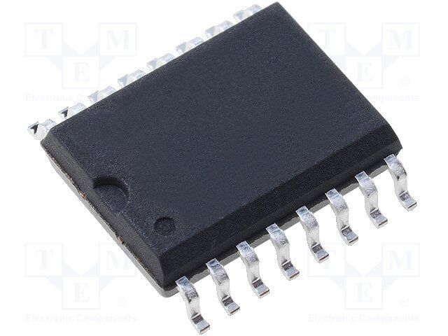
| 供应商器件封装 | 16-SOIC |
| 包装 | 管件 |
| 商标 | Analog Devices |
| 安装类型 | 表面贴装 |
| 安装风格 | SMD/SMT |
| 封装 | Tube |
| 封装/外壳 | 16-SOIC(0.295",7.50mm 宽) |
| 封装/箱体 | SOIC-16 |
| 工作电源电压 | 5 V |
| 工厂包装数量 | 47 |
| 带宽 | 4.4 MHz, 5.2 MHz |
| 应用 | RGB 至 NTSC/PAL |
| 最大功率耗散 | 800 mW |
| 最大工作温度 | + 85 C |
| 最小工作温度 | - 40 C |
| 标准包装 | 47 |
| 电压-电源,数字 | 4.75 V ~ 5.25 V |
| 电压-电源,模拟 | - |
| 电源电流 | 30 mA |
| 类型 | 视频编码器 |
| 系列 | AD725 |
| 通道数量 | 3 Channel |


PDF Datasheet 数据手册内容提取
a Low Cost RGB to NTSC/PAL Encoder with Luma Trap Port AD725 FEATURES PRODUCT DESCRIPTION Composite Video Output: Both NTSC and PAL The AD725 is a very low cost general purpose RGB to NTSC/ Chrominance and Luminance (S-Video) Outputs PAL encoder that converts red, green and blue color compo- Luma Trap Port to Eliminate Cross Color Artifacts nent signals into their corresponding luminance (baseband TTL Logic Levels amplitude) and chrominance (subcarrier amplitude and phase) Integrated Delay Line and Auto-Tuned Filters signals in accordance with either NTSC or PAL standards. Drives 75 (cid:86) Reverse-Terminated Loads These two outputs are also combined on-chip to provide a Low Power +5 V Operation composite video output. All three outputs are available sepa- Power-Down to <1 (cid:109)A rately at voltages of twice the standard signal levels as re- Very Low Cost quired for driving 75 W , reverse-terminated cables. APPLICATIONS The AD725 features a luminance trap (YTRAP) pin that pro- RGB/VGA to NTSC/PAL Encoding vides a means of reducing cross color generated by subcarrier Personal Computers/Network Computers frequency components found in the luminance signal. For por- Video Games table or other power-sensitive applications, the device can be Video Conference Cameras powered down to less than 1 m A of current consumption. All Digital Still Cameras logic levels are TTL compatible thus supporting the logic re- quirements of 3 V CMOS systems. The AD725 is packaged in a low cost 16-lead SOIC and oper- ates from a +5 V supply. FUNCTIONAL BLOCK DIAGRAM NTSC/PAL HSYNC SYNC CSYNC VSYNC XNOR CSYNC SEPARATOR 4FSC BURST NTSC/PAL 4FSC CLOCK FSC 908C 61808C FSC 908C/2708C 4FSC QUADRATURE (PAL ONLY) DEC+O4DER FSC 08C CLOCK CSYNC AT 8FSC RED CLDACMP Y L3FP-IPL POTRELERE- DSEALDMAAPYTL ALEIDN-E L2FP-I PLPOTOELSRET- X2 LOUUMTPINUATNCE LUMINANCE TRAP GREEN DC REGNBC-TOOD-IYNUGV U 4-LPPOFLE CLAUMP NTSC/PAL S X2 COOUMTPPUOTSITE CLAMP MATRIX BALANCED 4-POLE CHROMINANCE MODULATORS LPF X2 OUTPUT DC V 4-POLE V BLUE CLAMP LPF CLAMP BURST REV. 0 Information furnished by Analog Devices is believed to be accurate and reliable. However, no responsibility is assumed by Analog Devices for its use, nor for any infringements of patents or other rights of third parties One Technology Way, P.O. Box 9106, Norwood, MA 02062-9106, U.S.A. which may result from its use. No license is granted by implication or Tel: 781/329-4700 World Wide Web Site: http://www.analog.com otherwise under any patent or patent rights of Analog Devices. Fax: 781/326-8703 © Analog Devices, Inc., 1997
AD725–SPECIFICATIONS (Unless otherwise noted, V = +5, T = +25(cid:56)C, using 4FSC synchronous clock. All loads are S A 150 (cid:86) (cid:54) 5% at the IC pins. Outputs are measured at the 75 (cid:86) reverse terminated load.) Parameter Conditions Min Typ Max Units SIGNAL INPUTS (RIN, GIN, BIN) Input Amplitude Full Scale 714 mV p-p Black Level1 0.8 V Input Resistance2 RIN, GIN, BIN 1 MW Input Capacitance 5 pF LOGIC INPUTS (HSYNC, VSYNC, 4FSC, CE, STND) TTL Logic Levels Logic Low Input Voltage 1 V Logic High Input Voltage 2 V Logic Low Input Current (DC) 1 m A Logic High Input Current (DC) 1 m A VIDEO OUTPUTS3 Luminance (LUMA) Bandwidth, –3 dB NTSC 4.4 MHz PAL 5.2 MHz Gain Error –7 –2 +7 % Nonlinearity max p-p 0.3 % Sync Level NTSC 252 279 310 mV PAL 264 291 325 mV DC Black Level 1.3 V Luminance Trap (YTRAP) Output Resistance 1.0 kW DC Black Level 1.0 V Chrominance (CRMA) Bandwidth, –3 dB NTSC 1.2 MHz PAL 1.5 MHz Color Burst Amplitude NTSC 206 255 305 mV p-p PAL 221 291 362 mV p-p Color Burst Width NTSC 2.51 m s PAL 2.28 m s Chroma Level Error4 –4 % Chroma Phase Error5 – 3 Degrees DC Black Level 2.0 V Chroma Feedthrough R, G, B = 0 15 40 mV p-p Composite (COMP) Absolute Gain Error With Respect to Luma –5 –1 +3 % Differential Gain With Respect to Chroma 0.5 % Differential Phase With Respect to Chroma 1.5 Degrees DC Black Level 1.4 V Chroma/Luma Time Alignment S-Video 20 ns POWER SUPPLIES Recommended Supply Range Single Supply +4.75 +5.25 V Quiescent Current—Encode Mode 30 36 mA Quiescent Current—Power Down <1 m A NOTES 1R, G, and B signals are inputted via an external ac coupling capacitor. 2Except during dc restore period (back porch clamp). 3All outputs measured at a 75 W reverse-terminated load; ac voltages at the IC output pins are twice those specified here. 4Difference between ideal and actual color bar subcarrier amplitudes. 5Difference between ideal and actual color bar subcarrier phases. Specifications are subject to change without notice. –2– REV. 0
AD725 ABSOLUTE MAXIMUM RATINGS* PIN CONFIGURATION SupplyVoltage, APOS to AGND . . . . . . . . . . . . . . . . . . +6V 16-Lead Wide Body (SOIC) SupplyVoltage, DPOS to DGND . . . . . . . . . . . . . . . . . . +6V (R-16) AGND to DGND . . . . . . . . . . . . . . . . . . . . . –0.3 V to +0.3 V Inputs . . . . . . . . . . . . . . . . . . .DGND – 0.3 to DPOS + 0.3 V InternalPowerDissipation . . . . . . . . . . . . . . . . . . . . . .800 mW Operating Temperature Range . . . . . . . . . . . .–40(cid:176) C to +85(cid:176) C STND 1 16 HSYNC Storage Temperature Range . . . . . . . . . . . . .–65(cid:176) C to +125(cid:176) C AGND 2 15 VSYNC Lead Temperature Range (Soldering30sec) . . . . . . . . +230(cid:176) C 4FSC 3 14 DPOS APOS 4 AD725 13 DGND *Stresses above those listed under Absolute Maximum Ratings may cause perma- TOP VIEW nent damage to the device. This is a stress rating only; functional operation of the CE 5 (Not to Scale) 12 YTRAP device at these or any other conditions above those indicated in the operational RIN 6 11 LUMA section of this specification is not implied. Exposure to absolute maximum rating GIN 7 10 COMP conditions for extended periods may affect device reliability. BIN 8 9 CRMA Thermal Characteristics: 16-Pin SOIC Package: q = 100(cid:176)C/W. JA ORDERING GUIDE Temperature Package Package Model Range Description Option AD725AR –40(cid:176) C to +85(cid:176) C 16-Lead SOIC R-16 AD725AR-Reel –40(cid:176) C to +85(cid:176) C 16-Lead SOIC R-16 AD725AR-Reel7 –40(cid:176) C to +85(cid:176) C 16-Lead SOIC R-16 AD725-EB Evaluation Board CAUTION ESD (electrostatic discharge) sensitive device. Electrostatic charges as high as 4000V readily WARNING! accumulate on the human body and test equipment and can discharge without detection. Although the AD725 features proprietary ESD protection circuitry, permanent damage may occur on devices subjected to high energy electrostatic discharges. Therefore, proper ESD ESD SENSITIVE DEVICE precautions are recommended to avoid performance degradation or loss of functionality. REV. 0 –3–
AD725 PIN DESCRIPTIONS Pin Mnemonic Description Equivalent Circuit 1 STND Encoding Standard Pin. A Logic HIGH input selects NTSC encoding. Circuit A A Logic LOW input selects PAL encoding. TTL Logic Levels. 2 AGND Analog Ground Connection. 3 4FSC 4FSC Clock Input. Circuit A For NTSC: 14.318 180 MHz. For PAL: 17.734 475 MHz. TTL Logic Levels. 4 APOS Analog Positive Supply (+5 V – 5%). 5 CE Chip Enable. A Logic HIGH input enables the encode function. Circuit A A Logic LOW input powers down chip when not in use. TTL Logic Levels. 6 RIN Red Component Video Input. Circuit B 0 mV to 714 mV AC-Coupled. 7 GIN Green Component Video Input. Circuit B 0 mV to 714 mV AC-Coupled. 8 BIN Blue Component Video Input. Circuit B 0 mV to 714 mV AC-Coupled. 9 CRMA Chrominance Output.* Circuit C Approximately 1.8 V peak-to-peak for both NTSC and PAL. 10 COMP Composite Video Output.* Circuit C Approximately 2.5 V peak-to-peak for both NTSC and PAL. 11 LUMA Luminance plus CSYNC Output.* Circuit C Approximately 2 V peak-to-peak for both NTSC and PAL. 12 YTRAP Luminance Trap Filter Tap. Attach L-C resonant network to reduce cross-color artifacts. Circuit D 13 DGND Digital Ground Connection. 14 DPOS Digital Positive Supply (+5 V – 5%). 15 VSYNC Vertical Sync Signal (if using external CSYNC set at > +2 V). TTL Logic Levels. Circuit A 16 HSYNC Horizontal Sync Signal (or CSYNC signal). TTL Logic Levels. Circuit A *The Luminance, Chrominance and Composite Outputs are at twice normal levels for driving 75 W reverse-terminated lines. APOS DPOS DPOS DPOS APOS DPOS 1kV 12 1 6 9 3 7 10 AGND DGND 5 8 11 15 DGND DGND AGND DGND 16 VCLAMP Circuit A Circuit B Circuit C Circuit D Figure 1.Equivalent Circuits –4– REV. 0
Typical Characteristics–AD725 +5V COMPOSITE TESTKIGGT2RN0OA0N0LIX SYNC RAGDB7 2T5O COVMIPDOESOITE MOSONINTYOR GPELNAETRFAOTRIOMN RGB NENTSCCO/DPEARL PVMMO-1D3E5L4Q 3 75V 4FSC GENLOCK 75V FSC (43.4.537396O51R485MMHHzz) FSC H3P 43 3P1L4LA TEVKMT7R0O0NAIX OSCILLATOR WAVEFORM MONITOR Figure 2.Evaluation Setup 1.0 1.0 APL = 50.8% APL = 50.6% 525 LINE NTSC NO FILTERING 625 LINE PAL NO FILTERING SLOW CLAMP TO 0.00V @ 6.63ms SLOW CLAMP TO 0.00V @ 6.72ms 100 0.5 0.5 S 50 S VOLT IRE VOLT 0.0 0 0.0 –50 –0.5 –0.5 0 10 20 30 40 50 60 0 10 20 30 40 50 60 µs ms Figure 3.100% Color Bars, NTSC Figure 5.100% Color Bars, PAL Figure 4. 100% Color Bars on Vector Scope, NTSC Figure 6.100% Color Bars on Vector Scope, PAL REV. 0 –5–
AD725–Typical Characteristics 1.0 1.0 APL = 46.6% APL = 33.5% 525 LINE NTSC NO FILTERING 625 LINE PAL NO FILTERING SLOW CLAMP TO 0.00V SLOW CLAMP TO 0.00V @ 6.63ms 100 @ 6.72 ms 0.5 0.5 VOLTS 50 IRE VOLTS 0.0 0 0.0 –50 –0.5 –0.5 0 10 20 30 40 50 60 0 10 20 30 40 50 60 ms ms Figure 7.Modulated Pulse and Bar, NTSC Figure 9.Modulated Pulse and Bar, PAL 200mV 1ms 200mV 1ms Figure 8.Zoom on Modulated Pulse, NTSC Figure 10.Zoom on Modulated Pulse, PAL –6– REV. 0
AD725 1.0 1.0 APL = 48.2% APL = 48.2% 625 LINE PAL NO FILTERING 525 LINE NTSC NO FILTERING SLOW CLAMP TO 0.00V @ 6.63ms 100 SLOW CLAMP TO 0.00V @ 6.72ms 100 0.5 0.5 S 50 S 50 VOLT IRE VOLT IRE 0.5MHz 1MHz 2MHz 3MHz 4MHz 5MHz 1MHz 2MHz 3MHz 4MHz 5MHz 6MHz 0.0 0 0.0 0 –50 –50 –0.5 –0.5 0 10 20 30 40 50 60 0 10 20 30 40 50 60 ms ms Figure 11.Multiburst, NTSC Figure 14.Multiburst, PAL H TIMING MEASUREMENT RS–170A (NTSC) H TIMING (PAL) FIELD = 1 LINE = 22 LINE = 25 9.35ms 5.67ms 2.29ms 5.57ms 9.0 CYCLES 4.90ms 4.80ms 273.4mV 36.1 IRE 85ns 70ns 38.0 IRE 89ns 287.7mV 89ns AVERAGE $ 256 AVERAGE $ 256 Figure 12.Horizontal Timing, NTSC Figure 15.Horizontal Timing, PAL DG DP (NTSC) Wfm —> MOD 5 STEP DG DP (PAL) Wfm —> MOD 5 STEP DIFFERENTIAL GAIN (%) MIN = –0.05 MAX = 0.39 pk–pk/MAX = 0.44 DIFFERENTIAL GAIN (%) MIN = –0.06 MAX = 0.43 pk–pk = 0.49 0.00 0.07 –0.05 0.20 0.22 0.39 0.00 –0.06 0.15 0.23 0.43 0.38 0.5 0.5 0.4 0.4 0.3 0.3 0.2 0.2 0.1 0.1 0.0 0.0 –0.1 –0.1 –0.2 –0.2 DIFFERENTIAL PHASE (deg) MIN = –0.33 MAX = 1.17 pk–pk = 1.50 DIFFERENTIAL PHASE (deg) MIN = –0.44 MAX = 1.34 pk–pk = 1.79 0.00 –0.33 0.10 0.70 1.05 1.17 0.00 –0.44 –0.02 0.70 1.17 1.34 2.0 2.0 1.5 1.5 1.0 1.0 0.5 0.5 0.0 0.0 –0.5 –0.5 –1.0 –1.0 1ST 2ND 3RD 4TH 5TH 6TH 1ST 2ND 3RD 4TH 5TH 6TH Figure 13.Composite Output Differential Phase Figure 16.Composite Output Differential Phase and Gain, NTSC and Gain, PAL REV. 0 –7–
AD725 THEORY OF OPERATION Following the dc clamps, the RGB inputs are buffered and split The AD725 is a predominantly analog design, with digital logic into two signal paths for constructing the luminance and control of timing. This timing logic is driven by a external fre- chrominance outputs. quency reference at four times the color subcarrier frequency, Luminance Signal Path input into the 4FSC pin of the AD725. This frequency should The luminance path begins with the luma (Y) matrix. This be 14.318 180 MHz for NTSC encoding, and 17.734 475 MHz matrix combines the RGB inputs to form the brightness infor- for PAL encoding. The 4FSC input accepts standard TTL logic mation in the output video. The inputs are combined by the levels. The duty cycle of this input clock is not critical, but a fast- standard transformation edged clock should be used to prevent excessive jitter in the timing. Y = 0.299 · R + 0.587 · G + 0.114 · B The AD725 accepts two common sync standards, composite This equation describes the sensitivity of the human eye to the sync or separate horizontal and vertical syncs. To use an exter- individual component colors, combining them into one value of nal composite sync, a logic high signal is input to the VSYNC brightness. The equation is balanced so that full-scale RGB pin and the composite sync is input to the HSYNC pin. If sepa- inputs give a full-scale Y output. rate horizontal and vertical syncs are available, the horizontal sync can be input to the HSYNC pin and vertical sync to the Following the luma matrix, the composite sync is added. The VSYNC pin. Internally, the device XNORs the two sync inputs user-supplied sync (from the HSYNC and VSYNC inputs) is to combine them into one negative-going composite sync. latched into the AD725 at half the master clock rate, gating a sync pulse into the luminance signal. With the exception of The AD725 detects the falling sync pulse edges, and times their transitioning on the clock edges, the output sync timing will be width. A sync pulse of standard horizontal width will cause the in the same format as the input sync timing. The output sync insertion of a colorburst vector into the chroma modulators at level will depend on the encoding standard, 286 mV (40 IRE) the proper time. A sync pulse outside the detection range will for NTSC and 300 mV for PAL (voltages at the pin will be cause suppression of the color burst, and the device will enter its twice these levels). vertical blanking mode. During this mode, the on-chip RC time constants are verified using the input frequency reference, and In order to be time-aligned with the filtered chrominance signal the filter cutoff frequencies are retuned as needed. path, the luma signal must be delayed before it is output. The AD725 uses a sampled delay line to achieve this delay. The component color inputs, RIN, GIN and BIN, receive ana- log signals specifying the desired active video output. The full- Following the luma matrix and prior to this delay line, a prefilter scale range of the inputs is 0.714 mV (for either NTSC or PAL removes higher frequencies from the luma signal to prevent aliasing operation). External black level is not important as these inputs by the sampled delay line. This three-pole Bessel low-pass filter has are terminated externally, and then ac coupled to the AD725. a –3 dB frequency of 4.85 MHz for NTSC, 6 MHz for PAL. The AD725 contains on-chip RGB input clamps to restore the After the luma prefilter, the bandlimited luma signal is sampled dc level on-chip to match its single supply signal path. This dc onto a set of capacitors at twice the master reference clock rate. restore timing is coincident with the burst flag, starting approxi- After an appropriate delay, the data is read off the delay line, mately 5.5 m s after the falling sync edge and lasting for 2.5 m s. reconstructing the luma signal. The 8FSC oversampling of this During this time, the device should be driven with a black input. delay line limits the amount of jitter in the reconstructed sync output. The clocks driving the delay line are reset once per video line during the burst flag. The output of the luma path will remain unchanged during this period and will not respond to changing RGB inputs. NTSC/PAL POWER AND GROUNDS 4FSC CHVLSSOYYCNNKCC 4FXSNCOR CSYNC SEPSAYRNACTOR BCUSYRNSCT NTSC/PAL AG++N55DVV LAAONNGAALLICOOGG FSC 908C 61808C FSC 908C/2708C DGND LOGIC 4FSC QUADRATURE (PAL ONLY) NOTE: DEC+O4DER FSC 08C CLOCK TOHUET PLUUTMSIN AARNEC AET, CTOWMICPEO NSIOTREM AANLD L CEHVREOLSM IFNOARNCE CSYNC AT 8FSC DRIVING 75V REVERSE-TERMINATED LINES. RED CLDACMP Y L3FP-IPL POTRELERE- DSEALDMAAPYTL ALEIDN-E L2FP-I PLPOTOELSRET- X2 LOUUMTPINUATNCE LUMINANCE TRAP GREEN DC REGNBC-TOOD-IYNUGV U 4-LPPOFLE CLAUMP NTSC/PAL S X2 COOUMTPPUOTSITE CLAMP MATRIX BALANCED 4-POLE CHROMINANCE MODULATORS LPF X2 OUTPUT DC V 4-POLE V BLUE CLAMP LPF CLAMP BURST Figure 17.Functional Block Diagram –8– REV. 0
AD725 The reconstructed luma signal is then smoothed with a two pole level during this time. The offset cancellation occurs after each Bessel low-pass filter. This filter has a –3 dB bandwidth of falling sync edge, approximately 350 ns after the falling sync 5.25 MHz for NTSC, 6.5 MHz for PAL. A final buffer pro- edge, lasting for a period of 140 ns. If the inputs are unbalanced vides current drive for the LUMA output pin. during this time (for example, if a sync-on-green RGB input were used), there will be an offset in this chrominance response Chrominance Signal Path of the inputs during the remainder of the horizontal line, includ- The chrominance path begins with the U and V color-difference ing the colorburst. matrices. The AD725 uses U and V modulation vectors for NTSC and PAL (+U being defined as 0 degrees phase), simpli- The U signal is sampled by the sine clock and the V signal is fying the design compared to I and Q designs. The U and V ma- sampled by the cosine clock in the modulators, after which they trices combine the RGB inputs by the standard transformations: are summed to form the chrominance (C) signal. U = 0.493 · (B – Y) The chrominance signal then passes through a final four-pole V = 0.877 · (R – Y) modified Bessel low-pass filter to remove the harmonics of the switching modulation. This filter has a –3 dB frequency of The Y signal in these transformations is provided by the lumi- 4.4 MHz for NTSC and 5.9 MHz for PAL. A final buffer pro- nance matrix. vides current drive for the CRMA output pin. Before modulation, the U and V signals are prefiltered to pre- Composite Output vent aliasing. These four-pole modified Bessel low-pass filters To provide a composite video output, the separate (S-Video) have a –3 dB bandwidth of 1.2 MHz for NTSC and 1.5 MHz luminance and chrominance signal paths are summed. Prior to for PAL. summing, however, a filter tap for removing cross-color artifacts Between the prefilters and the modulators, the colorburst vec- in the receiver is provided. tors are added to the U and V signals. The colorburst levels are The luminance path contains a resistor, output pin (YTRAP), defined according to the encoding standard. For NTSC, the and buffer prior to entering the composite summer. By connecting colorburst is in the –U direction (with no V component) with a an inductor and capacitor on this pin, an R-L-C series-resonant resultant amplitude of 286 mV (40 IRE) at 180 degrees phase. circuit can be tuned to null out the luminance frequency For PAL, the colorburst has equal parts of –U and – V vectors response at the chrominance subcarrier frequency (3.579 545MHz (changing V phase every line) for a resultant amplitude of for NTSC, 4.433 618 MHz for PAL). The center frequency (f ) 300 mV alternating between 135 and 225 degrees phase (volt- C of this filter will be determined by the external inductor and ages at the pin will be twice these levels). capacitor by the equation: The burst gate timing is generated by waiting for a certain num- ber of reference clock cycles following the falling sync edge. If 1 f = the sync pulse width is measured to be outside the standard C 2p LC horizontal width, it is assumed that the device is in an h/2 period (vertical blanking interval) and the burst is suppressed. It can be seen from this equation that the center frequency of the trap is entirely dependent on external components. The U and V signals are used to modulate a pair of quadrature clocks (sine and cosine) at one-fourth the reference frequency The ratio of center frequency to bandwidth of the notch (Q = input (3.579 545 MHz for NTSC, 4.433618 MHz for PAL). f /BW) can be described by the equation: C For PAL operation, the phase of the cosine (V) clock is changed after each falling sync edge is detected. This will change the 1 L Q = V-vector phase in PAL mode every horizontal line. By driving 1000 C the AD725 with an odd number of sync edges per field, any individual line will flip phase each field as required by the standard. When choosing the Q of the filter, it should be kept in mind that the sharper the notch, the more critical the tolerance of the In order to suppress the carriers in the chrominance signal, the components must be in order to target the subcarrier frequency. U and V modulators are balanced. Once per horizontal line the Additionally, higher Q notches will exhibit a transient response offsets in the modulators are cancelled in order to minimize with more ringing after a luminance step. The magnitude of this residual subcarrier when the RGB inputs are equal. This offset ringing can be large enough to cause visible shadowing for Q cancellation also provides a dc restore for the U and V signal values much greater than 1.5. paths, so it is important that the RGB inputs be held at black REV. 0 –9–
AD725 HSYNC/VSYNC t (USER INPUTS) SW RIN/GIN BIN t (USER INPUTS) SB t SM MODULATOR RESTORE t MW INPUT CLAMPS tSR tRW BURST FLAG/ t t DELAY LINE RESET SD DW t t SS BY LUMA t BC t SC CRMA Figure 18.Timing Diagram (Not to Scale) Table I. Timing Description (See Figure 18) Symbol Name Description NTSC1 PAL2 t Sync Width Input valid sync width for burst Min 2.8 m s Min 3.3 m s SW insertion (user-controlled). Max 5.3 m s Max 5.4 m s t Sync to Blanking Minimum sync to color delay SB End (user-controlled). Min 8.2 m s Min 8.1 m s t Sync to Modulator Delay to modulator clamp start. SM Restore 392 ns 298 ns t Modulator Restore Length of modulator offset clamp MW Width (no chroma during this period). 140 ns 113 ns t Sync to RGB DC Delay to input clamping start. SR Restore 5.4 m s 5.6 m s t DC Restore Width Length of input clamp (no RGB RW response during this period). 2.5 m s 2.3 m s t Sync to Delay Line Delay to start of delay line SD Reset clock reset. 5.7 m s 5.8 m s t Delay Line Reset Length of delay line clock reset DW Width (no luma response during this period), also burst gate. 2.5 m s 2.3 m s t Sync Input to Luma Delay from sync input assertion SS Sync Output to sync in LUMA output. typ 310 ns typ 265 ns t Blanking End to Delay from RGB input assertion BY LUMA Start to LUMA output response. typ 340 ns typ 280 ns t Sync to Colorburst Delay from valid horizontal sync SC start to CRMA colorburst output. typ 5.8 m s typ 5.9 m s t Blanking End to Delay from RGB input assertion BC CRMA Start to CRMA output response. typ 360 ns typ 300 ns NOTES 1Input clock = 14.318180 MHz, STND pin = logic high. 2Input cock = 17.734475 MHz, STND pin = logic low. –10– REV. 0
AD725 APPLYING THE AD725 The AD725 will operate with subcarrier frequencies that deviate Inputs quite far from those specified by the TV standards. However, RIN, BIN, GIN are analog inputs that should be terminated to the monitor will in general not be quite so forgiving. Most moni- ground with 75 W in close proximity to the IC. When properly tors can tolerate a subcarrier frequency that deviates several hun- terminated the peak-to-peak voltage for a maximum input level dred Hz from the nominal standard without any degradation in should be 714 mV p-p. The horizontal blanking interval should picture quality. These conditions imply that the subcarrier fre- be the most negative part of each signal. quency accuracy is a system specification and not a specification The inputs should be held at the input signal’s black level dur- of the AD725 itself. ing the horizontal blanking interval. The internal dc clamps will The STND pin is used to select between NTSC and PAL opera- clamp this level during color burst to a reference that is used tion. Various blocks inside the AD725 use this input to program internally as the black level. Any noise present on the RIN, their operation. Most of the more common variants of NTSC and GIN, BIN or AGND pins during this interval will be sampled PAL are supported. There are, however, two known specific stan- onto the input capacitors. This can result in varying dc levels dards which are not supported by the standard AD725. These are from line to line in all outputs, or if imbalanced, subcarrier NTSC 4.43 and M-PAL. feedthrough in the COMP and CRMA outputs. Basically these two standards use most of the features of the For increased noise rejection, larger input capacitors are desired. standard that their names imply, but use the subcarrier that is A capacitor of 0.1 m F is usually adequate. equal to or approximately equal to the frequency of the other Similarly, the U and V clamps balance the modulators during an standard. Because of the automatic programming of the filters in interval shortly after the falling CSYNC input. Noise present the chrominance path and other timing considerations, a factory- during this interval will be sampled in the modulators, resulting programmed special version of the AD725 is necessary to sup- in residual subcarrier in the COMP and CRMA outputs. port these standards. HSYNC and VSYNC are two logic level inputs that are com- Layout Considerations The AD725 is an all CMOS mixed signal part. It has separate bined internally to produce a composite sync signal. If a com- pins for the analog and digital +5 V and ground power supplies. posite sync signal is to be used, it can be input to HSYNC while Both the analog and digital ground pins should be tied to the VSYNC is pulled to logic HI (> +2 V). ground plane by a short, low inductance path. Each power The form of the input sync signal(s) will determine the form of supply pin should be bypassed to ground by a low inductance the composite sync on the composite video (COMP) and lumi- 0.1 m F capacitor and a larger tantalum capacitor of about 10 m F. nance (LUMA) outputs. If no equalization or serration pulses The three analog inputs (RIN, GIN, BIN) should be terminated are included in the HSYNC input there won’t be any in the with 75 W to ground close to the respective pins. However, as outputs. Although sync signals without equalization and serra- these are high impedance inputs, they can be in a loop-through tion pulses do not technically meet the video standards’ specifi- configuration. This technique is used to drive two or more cations, many monitors do not require these pulses in order to devices with high frequency signals that are separated by some display good pictures. The decision whether to include these distance. A connection is made to the AD725 with no local signals is a system trade-off between cost and complexity and termination, and the signals are run to another distant device adhering strictly to the video standards. where the termination for these signals is provided. The HSYNC and VSYNC logic inputs have a small amount of The output amplitudes of the AD725 are double that required built-in hysteresis to avoid interpreting noisy input edges as by the devices that it drives. This compensates for the halving of multiple sync edges. This is critical to proper device operation, as the signal levels by the required terminations. A 75 W series the sync pulses are timed for vertical blanking interval detection. resistor is required close to each AD725 output, while 75 W to The logic inputs have been designed for VIL < 1.0 V and VIH ground should terminate the far end of each line. >2.0 V for the entire temperature and supply range of opera- The outputs have a dc bias and must be ac coupled for proper tion. This allows the AD725 to directly interface to TTL or 3 V operation. The COMP and LUMA outputs have information CMOS compatible outputs, as well as 5 V CMOS outputs down to 30 Hz for NTSC (25 MHz for PAL) that must be trans- where VOL is less than 1.0 V. mitted. Each output requires a 220 m F series capacitor to work The NTSC specification calls for a frequency accuracy of – 10 Hz with the 75 W resistance to pass these low frequencies. The CRMA from the nominal subcarrier frequency of 3.579545 MHz. While signal has information mostly up at the chroma frequency and maintaining this accuracy in a broadcast studio might not be a can use a smaller capacitor if desired, but 220 m F can be used to severe hardship, it can be quite expensive in a low cost con- minimize the number of different components used in the design. sumer application. REV. 0 –11–
AD725 Displaying VGA Output on a TV system, the internal 4FSC (14.318 180 MHz) clock that drives The AD725 can be used to convert the analog RGB output from a the VGA controller can be used for 4FSC on the AD725. This personal computer’s VGA card to the NTSC or PAL television signal is not directly accessible from outside the computer, but it standards. To accomplish this it is important to understand that does appear on the VGA card. (A 1FSC-input encoder, the the AD725 requires interlaced RGB video and clock rates that AD724, is also available.) are consistent with those required by the television standards. If a separate RGB monitor is also to be used, it is not possible to In most computers the default output is a noninterlaced RGB simply connect it to the R, G and B signals. The monitor pro- signal at a frame rate higher than used by either NTSC or PAL. vides a termination that would double terminate these signals. Most VGA controllers support a wide variety of output modes The R, G, and B signals should be buffered by three amplifiers that are controlled by altering the contents of internal registers. with high input impedances. These should be configured for a It is best to consult with the VGA controller manufacturer to gain of two, which is normalized by the divide by two termina- determine the exact configuration required to provide an inter- tion scheme used for the RGB monitor. laced output at 60 Hz (50 Hz for PAL). The AD8073 is a low cost triple video amplifier that can pro- Figure 19 shows a circuit for connection to the VGA port of a vide the buffering required in this application. However, since PC. The RGB outputs are ac coupled to the respective inputs of the R, G and B signals go all the way to ground during horizon- the AD725. These signals should each be terminated to ground tal sync, the AD8073 will require a –5 V supply to handle these with 75 W . signals. To be able to buffer the R, G and B signals using a single supply, a rail-to-rail amplifier is required. In this applica- The standard 15-pin VGA connector has HSYNC on Pin 13 tion, the AD8051 (single) and AD8052 (dual) can be used to and VSYNC on Pin 14. These signals also connect directly to provide the three required channels. These can be operated on a the same name signals on the AD725. For a synchronous NTSC single supply of 3 V to 5 V. +5V +5V 10mF 0.1mF 4 14 0.1mF 10mF APOS DPOS POWER DOWN 5 CE 0.1mF 0.1mF 6 RIN 75V COMPOSITE 0.1mF 7 GIN CMPS 10 220mF VIDEO AD725 8 BIN 16 HSYNC 75V Y 15 VSYNC LUMA 11 75V 75V 75V +5V 220mF 4FSC CLOCK OSC 4FSC 14.318180MHz (NTSOCR) 0.1mF CRMA 9 75V C 17.734475MHz (PAL) 220mF STND 47kV 9pF 68mH NTSC/PAL YTRAP S-VIDEO (Y/C VIDEO) 1N4148 18pF +5V (VAA) AGND DGND 0.1mF 2 13 VGA OUTPUT CONNECTOR 75V 1/3 AD8073 1kV 1kV VSYNC FROM VGA PORT 1/3 75V HSYNC AD8073 B 75V 1kV 1kV G 75V 1/3 75V AD8073 R 75V 0.1mF –5V 1kV 1kV RGB MONITOR Figure 19.Interfacing the AD725 to the (Interlaced) VGA Port of a PC –12– REV. 0
AD725 Low Cost Crystal Oscillator to as S-video or Y/C video. Since the luminance and chromi- A low cost oscillator can be made that provides a CW clock that nance are already separated, the monitor does not have to per- can be used to drive both the AD725 4FSC and other devices in form this function. The S-video outputs of the AD725 can be the system that require a clock at this frequency. Figure 20 shows a used to create higher quality pictures when there is an S-video circuit that uses one inverter of a 74HC04 package to create a input available on the monitor. crystal oscillator and another inverter to buffer the oscillator Flicker and drive other loads. The logic family must be a CMOS type In a VGA conversion application, where the software controlled that can support the frequency of operation, and it must NOT registers are correctly set, there are two techniques that are be a Schmitt trigger type of inverter. Resistor R1 from input to commonly used by VGA controller manufacturers to generate output of U1A linearizes the inverter’s gain such that it provides the interlaced signal. Each of these techniques introduces a useful gain and a 180 degree phase shift to drive the oscillator. unique characteristic into the display created by the AD725. The artifacts described below are not due to the encoder or its R1 1MV encoding algorithm as all encoders will generate the same dis- play when presented with these inputs. They are due to the TO PIN 3 U1A U1B OF AD725 method used by the controller display chip to convert a non- HC04 HC04 interlaced output to an interlaced signal. R2 TO OTHER Y1 200V DEVICE CLOCKS The first interlacing technique outputs a true interlaced signal with odd and even fields (one each to a frame Figure 21a). This ~(1O5PCpTF3) C471pF C602pF pCrDov vididees ot haen db easnt ipmicattuiorne q(guaamliteys ,w ehtecn.) .d Hispolwaeyvinegr, pith owtiollg irnatprhoy-, duce a defect commonly referred to as flicker into the display. Figure 20.Low Cost Crystal Oscillator Flicker is a fundamental defect of all interlaced displays and is The crystal should be a parallel resonant type at the appropriate caused by the alternating field characteristic of the interlace frequency (NTSC/PAL, 4FSC). The series combination of C1 technique. Consider a one pixel high black line which extends and C2 should approximately equal to the crystal manufacturer’s horizontally across a white screen. This line will exist in only specification for the parallel capacitance required for the crystal one field and will be refreshed at a rate of 30 Hz (25 Hz for to operate at its specified frequency. C1 will usually want to be PAL). During the time that the other field is being displayed the a somewhat smaller value because of the input parasitic capaci- line will not be displayed. The human eye is capable of detect- tance of the inverter. If it is desired to tune the frequency to ing this, and the display will be perceived to have a pulsating or greater accuracy, C1 can be made still smaller and a parallel flickering black line. This effect is highly content sensitive and adjustable capacitor can be used to adjust the frequency to the is most pronounced in applications in which text and thin desired accuracy. horizontal lines are present. In applications such as CD video, photography and animation, portions of objects naturally Resistor R2 serves to provide the additional phase shift occur in both odd and even fields and the effect of flicker is required by the circuit to sustain oscillation. It can be sized by R2 = 1/(2 · p · f · C2). Other functions of R2 are to provide a imperceptible. low pass filter that suppresses oscillations at harmonics of the The second commonly used technique is to output an odd and fundamental of the crystal and to isolate the output of the in- even field that are identical (Figure 21b). This ignores the data verter from the resonant load that the crystal network presents. that naturally occurs in one of the fields. In this case the same one pixel high line mentioned above would either appear as a The basic oscillator described above is buffered by U1B to drive two pixel high line, (one pixel high in both the odd and even field) the AD725 4FSC pin and other devices in the system. For a or not appear at all if it is in the data that is ignored by the control- system that requires both an NTSC and PAL oscillator, the ler. Which of these cases occurs is dependent on the placement circuit can be duplicated by using a different pair of inverters of the line on the screen. This technique provides a stable (i.e., from the same package. nonflickering) display for all applications, but small text can be Dot Crawl difficult to read and lines in drawings (or spreadsheets) can There are numerous distortions that are apparent in the presen- disappear. As above, graphics and animation are not particularly tation of composite signals on TV monitors. These effects will affected although some resolution is lost. vary in degree depending on the circuitry used by the monitor There are methods to dramatically reduce the effect of flicker and to process the signal and on the nature of the image being dis- maintain high resolution. The most common is to ensure that played. It is generally not possible to produce pictures on a display data never exists solely in a single line. This can be accom- composite monitor that are as high quality as those produced by plished by averaging/weighting the contents of successive/multiple standard quality RGB, VGA monitors. noninterlaced lines prior to creating a true interlaced output (Fig- One well known distortion of composite video images is called ure 21c). In a sense, this provides an output that will lie between dot crawl. It shows up as a moving dot pattern at the interface the two extremes described above. The weight or percentage of between two areas of different color. It is caused by the inability one line that appears in another, and the number of lines used, of the monitor circuitry to adequately separate the luminance are variables that must be considered in developing a system of and chrominance signals. this type. If this type of signal processing is performed, it must One way to prevent dot crawl is to use a video signal that has be completed prior to the data being presented to the AD725 separate luminance and chrominance. Such a signal is referred for encoding. REV. 0 –13–
AD725 Vertical Scaling NONINTERLACED ODD FIELD EVEN FIELD In addition to converting the computer generated image from 1 1 noninterlaced to interlaced format, it is also necessary to scale 2 2 3 3 the image down to fit into NTSC or PAL format. The most 4 = + 4 common vertical lines/screen for VGA display are 480 and 600 5 5 lines. NTSC can only accommodate approximately 400 visible 6 6 7 7 lines/frame (200 per field), PAL can accommodate 576 lines/ frame (288 per field). If scaling is not performed, portions of a. Conversion of Noninterlace to Interlace the original image will not appear in the television display. This line reduction can be performed by merely eliminating NONINTERLACED ODD FIELD EVEN FIELD every Nth (6th line in converting 480 lines to NSTC or every 1 1 2 2 25th line in converting 600 lines to PAL). This risks generation 3 3 of jagged edges and jerky movement. It is best to combine the 4 = + 4 scaling with the interpolation/averaging technique discussed 5 5 6 6 above to ensure that valuable data is not arbitrarily discarded in 7 7 the scaling process. Like the flicker reduction technique men- tioned above, the line reduction must be accomplished prior to b. Line Doubled Conversion Technique the AD725 encoding operation. NONINTERLACED ODD FIELD EVEN FIELD There is a new generation of VGA controllers on the market 1 1 specifically designed to utilize these techniques to provide a 2 2 crisp and stable display for both text and graphics oriented 3 3 applications. In addition these chips rescale the output from the 4 = + 4 5 5 computer to fit correctly on the screen of a television. A list of 6 6 known devices is available through Analog Devices’ Applica- 7 7 tions group, but the most complete and current information will c. Line Averaging Technique be available from the manufacturers of graphics controller ICs. Figure 21. Synchronous vs. Asynchronous Operation The source of RGB video and synchronization used as an input LUMA TRAP-THEORY to the AD725 in some systems is derived from the same clock The composite video output of the AD725 can be improved for signal as used for the AD725 subcarrier input (4FSC). These some types of images by incorporating a luma trap (or Y-Trap) systems are said to be operating synchronously. In systems in the encoder circuit. The basic configuration for such a circuit where two different clock sources are used for these signals, the is a notch or band elimination filter that is centered at the operation is called asynchronous. subcarrier frequency. The luma trap is only functional for the composite video output of the AD725; it has no influence on The AD725 supports both synchronous and asynchronous the S-Video (or Y/C-Video) output. operation, but some minor differences might be noticed be- tween them. These can be caused by some details of the inter- The need for a luma trap arises from the method used by com- nal circuitry of the AD725. posite video to encode the color part (chrominance or chroma) of the video signal. This is performed by amplitude and phase There is an attempt to process all of the video and synchroniza- modulation of a subcarrier. The saturation (or lack of dilution of tion signals totally asynchronous with respect to the subcarrier a color with white) is represented in the subcarrier’s amplitude signal. This was achieved everywhere except for the sampled modulation, while the hue (or color as thought of as the sections delay line used in the luminance channel to time align the lumi- of a rainbow) information is contained in the subcarrier’s phase nance and chrominance. This delay line uses a signal at eight modulation. The modulated subcarrier occupies a bandwidth times the subcarrier frequency as its clock. somewhat greater than 1 MHz depending on the video standard. The phasing between the delay line clock and the luminance For a composite signal, the chroma is linearly added to the signal (with inserted composite sync) will be constant during luminance (luma or brightness) plus sync signal to form a single synchronous operation, while the phasing will demonstrate a composite signal with all of the picture information. Once this periodic variation during asynchronous operation. The jitter of addition is performed, it is no longer possible to ascertain which the asynchronous video output will be slightly greater due to component contributed which part of the composite signal. these periodic phase variations. At the receiver, this single composite signal must be separated into its various parts to be properly processed. In particular, the chroma must be separated and then demodulated into its or- thogonal components, U and V. Then, along with the luma signal, the U and V signals generate the RGB signals that con- trol the three video guns in the monitor. A basic problem arises when the luma signal (which contains no color information) contains frequency components that fall –14– REV. 0
AD725 within the chroma band. All signals in this band are processed quality. S-video will not just eliminate cross chrominance, but as chroma information since the chroma processing circuit has will also not have this notch in the luma response. no knowledge as to where these signals originated. Therefore, Implementing a Luma Trap the color that results from the luma signals in the chroma band The AD725 implementation of a luma trap uses an on-chip is a false color. This effect is referred to as cross chrominance. resistor along with an off-chip inductor and capacitor to create The cross chrominance effect is sometimes evident in white text an RLC notch filter. The filter must be tuned to the center on a black background as a moving rainbow pattern around the frequency of the video standard being output by the AD725, characters. The sharp transitions from black to white (and vice 3.58MHz for NTSC or 4.43 MHz for PAL. versa) that comprise the text dots contain frequency compo- The circuit is shown in Figure 22. The 1 kW series resistor in nents across the whole video band, and those in the chroma the composite video luma path on the AD725 works against the band create cross chrominance. This is especially pronounced impedance of the off-chip series LC to form a notch filter. The when the dot clock used to generate the characters is an integer frequency of the filter is given by: multiple of the chroma subcarrier frequency. Another common contributor to cross chrominance effects is f = 1 certain striped clothing patterns that are televised. At a specific 2p LC amount of zoom, the spatial frequency of vertical stripe patterns will generate luma frequencies in the chroma band. These fre- CRMA 220mF 75V quency components will ultimately get turned into color by the video monitor. Since the phase of these signals is not coherent A AD725 COMP 220mF 75V with the subcarrier, the effect shows up as random colors. If the 14.318180MHz zoom of a TV camera is modified or there is motion of the B 4FSC LUMA 220mF 75V striped pattern, the false colors can vary quite radically and 17.734475MHz produce a quite objectionable “moving rainbow” effect. Most A/B LUMA 1.0kV TV-savvy people have learned to adapt by just not wearing STND YTRAP certain patterns when appearing on TV. An excellent way to eliminate virtually all cross chrominance C2 L effects is to use S-video. Since the luma and chroma are carried 47kV 9pF 68mH on two separate circuits, there is no confusion as to which cir- NTSC/PAL D1 C1 cuit should process which signals. Unfortunately, not all TVs 1N4148 18pF that exist today, and probably still not even half of those being sold, have a provision for S-video input. Figure 22.Luma Trap Circuit for NTSC and PAL Video To ensure compatibility with the input capabilities of the major- Dual-Standard Luma Trap ity of TVs in existence, composite video must be supplied. For a filter that will work for both PAL and NTSC a means is Many more TVs have a composite baseband video input port required to switch the tuning of the filter between the two than have an S-video port to connect cameras and VCRs. subcarrier frequencies. The PAL standard requires a higher However, still the only common denominator for virtually all frequency than NTSC. A basic filter can be made that is tuned TVs is an RF input. This requires modulating the baseband to the PAL subcarrier and a simple diode circuit can then be video onto an RF carrier that is usually tuned to either Channel used to switch in an extra parallel capacitor that will lower the 3 or 4 (for NTSC). Most video games that can afford only a filter’s frequency for NTSC operation. single output use an RF interface because of its universality. Figure 22 shows how the logic signal that drives STND (Pin 1) Sound can also be carried on this channel. can also be used to drive the circuit that selects the tuning of the Since it is not practical to rely exclusively on S-video to improve luma trap circuit. When the signal applied to STND (Pin 1) is the picture quality by eliminating cross chrominance, a luma low (ground), the PAL mode is selected. This results in a bias of trap can be used to minimize this effect for systems that use 0 V across D1, which is an off condition. As a result, C2 is out composite video. The luma trap notches out or “traps” the of the filter circuit and only C1 tunes the notch filter to the PAL offending frequencies from the luma signal before it is added to subcarrier frequency, 4.43 MHz. the chroma. The cross chrominance that would be generated by On the other hand, when STND is high (+5 V), NTSC is se- these frequencies is thereby significantly attenuated. lected and there is a forward bias across D1. This turns the The only sacrifice that results is that the luma response has a diode on and adds C2 in parallel with C1. The notch filter is “hole” in it at the chroma frequency. This will lower the lumi- now tuned to the NTSC subcarrier frequency, 3.58 MHz. nance resolution of details whose spatial frequency causes frequency components in the chroma band. However, the attenuation of cross chrominance outweighs this in the picture REV. 0 –15–
AD725 Measuring the Luma Trap Frequency Response tarily apply an HSYNC signal to reset the timing and perform The frequency response of the luma trap can be measured in the dc restore. Because the inputs are high-impedance, the two different ways. The first involves using an RGB frequency droop during testing will be minimal. It is not desirable to apply sweep input pattern into the AD725 and observing the compos- a steady pulse train of HSYNC inputs because the spectrum of ite output on a TV monitor, a TV waveform monitor or on an these pulses will show up in the output response. oscilloscope. A more stable, low noise method is shown in Figure 23. The On a TV monitor, the composite video display will look like RGB inputs are biased using a power supply and the source port vertical black and white lines that are coarsely spaced (low fre- bias input of the network analyzer. A momentary sync input is quency) on the left side and progress to tightly spaced (high still applied to the device to reset its internal timing, but droop frequency) on the right side. Somewhere to the right of center, during testing will no longer be an issue. there will not be discernible stripes, but rather only a gray verti- The signal source is applied to the GIN input for largest output cal area. This is the effect of the luma trap, which filters out response. This input should be terminated through the appro- luminance detail at a band of frequencies. priate termination resistor (matching the output impedance of At the bottom of the display are markings at each megahertz the network analyzer). If necessary, calibration inaccuracies can that establish a scale of frequency vs. horizontal position. The be flattened out by reading back the input reference using a location of the center of the gray area along the frequency FET probe. marker scale indicates the range of frequencies that are being filtered out. The gray area should be about halfway between the NETWORK ANALYZER 3 MHz and 4 MHz markers for NTSC, and about halfway SOURCE between the 4 MHz and 5 MHz markers for PAL. REF SOURCE MEASURE BIAS When a horizontal line is viewed on an oscilloscope or video 1V FET waveform monitor, the notch in the response will be apparent. PROBE OUT 15V 15V The frequency will have to be interpolated from the location of IN the notch position along the H-line. 1 1 10mF 0.1mF 0.1mF 10mF 1.0 4 14 7 GIN APOS DPOS 100 75V 220mF 75V 1 COMP 6 RIN 0.5 50 8 BIN AD725 TS 1V VOL IRE 15V 15 VSYNC CRMA 9 NC 15V 0.0 0 LUMA 11 NC MOMENTARY 10kV CSYNC 16 HSYNC ENCD 5 15V –50 OSC 4FSC –0.5 0 10 20 30 40 50 60 STND ms NTSC/PAL YTRAP Figure 23.Luminance Sweep with Trap, COMP Pin 47kV 68mH AGND DGND The second method involves using a network analyzer to mea- 9pF 2 13 sure the frequency response of the composite signal. In order to NC = NO CONNECT 1N4148 18pF perform this successfully, the AD725 must be given the appro- priate signals so that it will pass video signals through it. Figure 24 illustrates the setup used for these measurements. Figure 24.Measurement Setup for Determining Luma Trap Frequency The first requirement is that the part must receive a subcarrier clock. This will provide clocking to the internal delay line and The composite output is reverse terminated with a 50 W or 75W enable it to pass the video signal. The subcarrier clock should be resistor and input to the measuring channel of a network analyzer. at the 4FSC frequency for either NTSC or PAL. Since only the green input is driven, this method does not yield The second requirement is that the RGB inputs are properly an absolute measurement of composite signal levels, but the biased for linear operation, and the timing logic is properly notch in the composite output will be readily discernible. The reset. It is acceptable to ac-couple the RGB inputs and momen- frequency measuring functions of the network analyzer can then be use to accurately measure the frequency of the luma notch filter (luma trap). –16– REV. 0
AD725 6 signal should occur at the output of an on-chip XNOR gate on the AD725 whose two inputs are HSYNC (Pin 16) and VSYNC 3 (Pin 15). There are several options for meeting these conditions. 0 LUMA PIN The first is to have separate signals for HSYNC and VSYNC. –3 Each should be mostly low and then high going during their COMP PIN B d–6 respective time of assertion. This is the convention used by – AIN –9 RGB monitors for most PCs. The proper composite sync signal G will be produced by the on-chip XNOR gate when using these –12 inputs. –15 If a composite sync signal is already available, it can be input –18 into HSYNC (Pin 16), while VSYNC (Pin 15) can be used to –21 change the polarity. (In actuality, HSYNC and VSYNC are interchangeable since they are symmetric inputs to a two-input –24 0.1 1.0 10.0 gate). FREQUENCY – MHz Figure 25.Luminance Frequency Response with NTSC Trap If the composite sync input is mostly high and then low going for active HSYNC time (and inverted duty cycle during VSYNC), SYNCHRONIZING SIGNALS then it is already of the proper polarity. Pulling VSYNC high, The AD725 requires explicit horizontal and vertical synchroniz- while inputting the composite sync signal to HSYNC will pass ing signals for proper operation. This information cannot and this signal though the XNOR gate without inversion. should not be incorporated in any of the RGB signals. However, On the other hand, if the composite sync signal is the opposite the synchronizing information can be provided as either separate polarity as described above, pulling VSYNC low will cause the horizontal (HSYNC) and vertical (VSYNC) signals or as a XNOR gate to invert the signal. This will make it the proper single composite sync (CSYNC) signal. polarity for use inside the AD725. These logic conditions are Internally the AD725 requires a composite sync logic signal that illustrated in Figure 26. is mostly high and goes low during horizontal sync time. The vertical interval will have an inverted duty cycle from this. This HSYNC VSYNC CSYNC Figure 26.Sync Logic Levels (Equalization and Serration Pulses Not Shown) REV. 0 –17–
AD725 OUTLINE DIMENSIONS Dimensions shown in inches and (mm). 16-Lead Wide Body SOIC (R-16) 0.4133 (10.50) 0.3977 (10.00) 16 9 1 8 0.2992 (7.60)0.2914 (7.40) 0.4193 (10.65)0.3937 (10.00) PIN 1 0.1043 (2.65) 0.0291 (0.74) 0.0118 (0.30) 0.0926 (2.35) 0.0098 (0.25)x 45° 0.0040 (0.10) 8° 0.0500 (1.27) 0(B.10.S52C070) 00..00119328 ((00..4395)) SPELAANTIENG 00..00102951 ((00..3223))0° 0.0157 (0.40) –18– REV. 0
–19–
7 9 0/ 1 – 8 – 9 9 1 3 C A. S. U. N D I E T N RI P –20–