ICGOO在线商城 > 集成电路(IC) > 数据采集 - 数模转换器 > AD7245AAN
 Datasheet下载
- 型号: AD7245AAN
- 制造商: Analog
- 库位|库存: xxxx|xxxx
- 要求:
| 数量阶梯 | 香港交货 | 国内含税 |
| +xxxx | $xxxx | ¥xxxx |
查看当月历史价格
查看今年历史价格
AD7245AAN产品简介:
ICGOO电子元器件商城为您提供AD7245AAN由Analog设计生产,在icgoo商城现货销售,并且可以通过原厂、代理商等渠道进行代购。 AD7245AAN价格参考。AnalogAD7245AAN封装/规格:数据采集 - 数模转换器, 12 位 数模转换器 1 24-PDIP。您可以下载AD7245AAN参考资料、Datasheet数据手册功能说明书,资料中有AD7245AAN 详细功能的应用电路图电压和使用方法及教程。
| 参数 | 数值 |
| 产品目录 | 集成电路 (IC)半导体 |
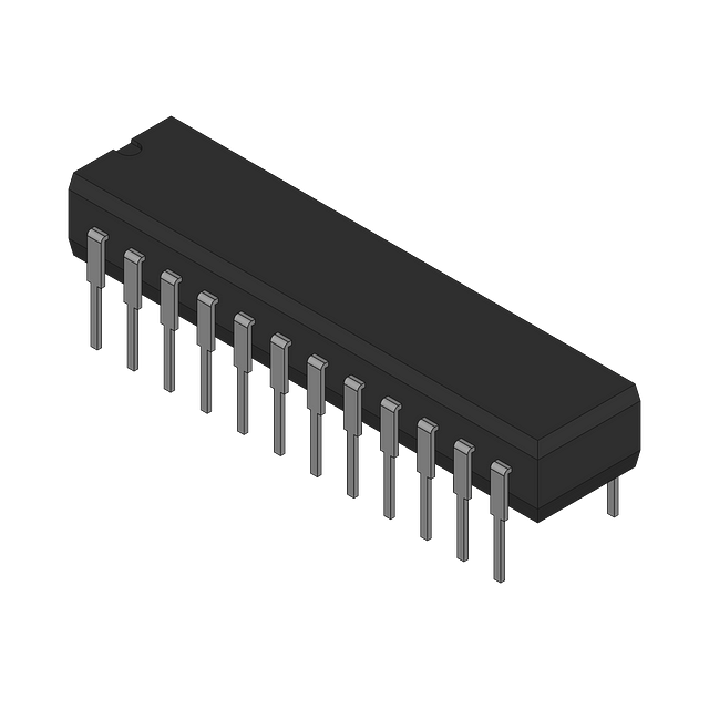
| 描述 | IC DAC 12BIT LC2MOS 24-DIP数模转换器- DAC 12B V-OUT IC w/ Dbl Buffrd Parallel Inpt |
| 产品分类 | |
| 品牌 | Analog Devices Inc |
| 产品手册 | |
| 产品图片 |
|
| rohs | 否含铅 / 不符合限制有害物质指令(RoHS)规范要求 |
| 产品系列 | 数据转换器IC,数模转换器- DAC,Analog Devices AD7245AANDACPORT® |
| 数据手册 | |
| 产品型号 | AD7245AAN |
| 产品培训模块 | http://www.digikey.cn/PTM/IndividualPTM.page?site=cn&lang=zhs&ptm=19145http://www.digikey.cn/PTM/IndividualPTM.page?site=cn&lang=zhs&ptm=18614http://www.digikey.cn/PTM/IndividualPTM.page?site=cn&lang=zhs&ptm=26125http://www.digikey.cn/PTM/IndividualPTM.page?site=cn&lang=zhs&ptm=26140http://www.digikey.cn/PTM/IndividualPTM.page?site=cn&lang=zhs&ptm=26150http://www.digikey.cn/PTM/IndividualPTM.page?site=cn&lang=zhs&ptm=26147 |
| 产品种类 | 数模转换器- DAC |
| 位数 | 12 |
| 供应商器件封装 | 24-PDIP |
| 分辨率 | 12 bit |
| 包装 | 管件 |
| 商标 | Analog Devices |
| 安装类型 | 通孔 |
| 安装风格 | Through Hole |
| 封装 | Tube |
| 封装/外壳 | 24-DIP(0.300",7.62mm) |
| 封装/箱体 | PDIP-24 |
| 工作温度 | -40°C ~ 85°C |
| 工厂包装数量 | 15 |
| 建立时间 | 7µs |
| 接口类型 | Parallel |
| 数据接口 | 并联 |
| 最大功率耗散 | 450 mW |
| 最大工作温度 | + 85 C |
| 最小工作温度 | - 40 C |
| 标准包装 | 15 |
| 电压参考 | 5 V |
| 电压源 | 双 ± |
| 电源电压-最大 | 16.5 V |
| 电源电压-最小 | 10.8 V |
| 积分非线性 | +/- 1 LSB |
| 稳定时间 | 10 us |
| 系列 | AD7245A |
| 结构 | R-2R |
| 转换器数 | 1 |
| 转换器数量 | 1 |
| 输出数和类型 | 1 电压,单极1 电压,双极 |
| 输出类型 | Voltage Buffered |
| 采样比 | 143 kSPs |
| 采样率(每秒) | 143k |


PDF Datasheet 数据手册内容提取
a LC2MOS 12-Bit DACPORTs AD7245A/AD7248A FEATURES AD7245A FUNCTIONAL BLOCK DIAGRAM 12-Bit CMOS DAC with Output Amplifier and VDD REF OUT ROFS Reference Improved AD7245/AD7248: 2R 2R 12 V to 15 V Operation RFB (cid:1)1/2 LSB Linearity Grade VOUT Faster Interface—30 ns Typ Data Setup Time Extended Plastic Temperature Range (–40(cid:2)C to +85(cid:2)C) VREF DAC AGND VSS Single or Dual Supply Operation Low Power—65 mW Typ in Single Supply Parallel Loading Structure: AD7245A CS DAC LATCH CLR (8+4) Loading Structure: AD7248A CONTROL WR LOGIC AD7245A GENERAL DESCRIPTION The AD7245A/AD7248A is an enhanced version of the industry LDAC INPUT LATCH standard AD7245/AD7248. Improvements include operation from 12 V to 15 V supplies, a ±1/2 LSB linearity grade, faster interface times and better full scale and reference variations with V . Additional features include extended temperature range DB0 DB11 DGND DD operation for commercial and industrial grades. AD7248A FUNCTIONAL BLOCK DIAGRAM The AD7245A/AD7248A is a complete, 12-bit, voltage output, digital-to-analog converter with output amplifier and Zener voltage VDD REF OUT ROFS reference on a monolithic CMOS chip. No external user trims 2R 2R are required to achieve full specified performance. RFB Both parts are microprocessor compatible, with high speed data latches and double-buffered interface logic. The AD7245A accepts VOUT 12-bit parallel data that is loaded into the input latch on the VREF DAC rising edge of CS or WR. The AD7248A has an 8-bit-wide data AGND VSS bus with data loaded to the input latch in two write operations. For both parts, an asynchronous LDAC signal transfers data LDAC DAC LATCH from the input latch to the DAC latch and updates the analog output. The AD7245A also has a CLR signal on the DAC latch WR CONTROL AD7248A LOGIC CSLSB which allows features such as power-on reset to be implemented. 4-BIT 8-BIT CSMSB INPUT INPUT The on-chip 5 V buried Zener diode provides a low noise, tem- LATCH LATCH perature compensated reference for the DAC. For single supply operation, two output ranges of 0 V to 5 V and 0 V to 10 V are available, while these two ranges plus an additional ±5 V range DB7 DB0 DGND are available with dual supplies. The output amplifiers are capa- ble of developing 10 V across a 2 kΩ load to GND. PRODUCT HIGHLIGHTS The AD7245A/AD7248A is fabricated in linear compatible CMOS 1. The AD7245A/AD7248A is a 12-bit DACPORT® on a single (LC2MOS), an advanced, mixed technology process that combines chip. This single chip design and small package size offer precision bipolar circuits with low power CMOS logic. The considerable space saving and increased reliability over AD7245A is available in a small, 0.3" wide, 24-lead DIP and multichip designs. SOIC and in 28-terminal surface mount packages. The AD7248A 2. The improved interface times on the part allows easy, direct is packaged in a small, 0.3" wide, 20-lead DIP and SOIC and in interfacing to most modern microprocessors. 20-terminal surface mount packages. 3. The AD7245A/AD7248A features a wide power supply range allowing operation from 12 V supplies. DACPORT is a registered trademark of Analog Devices, Inc. REV.B Information furnished by Analog Devices is believed to be accurate and reliable. However, no responsibility is assumed by Analog Devices for its use, nor for any infringements of patents or other rights of third parties One Technology Way, P.O. Box 9106, Norwood, MA 02062-9106, U.S.A. which may result from its use. No license is granted by implication or Tel: 781/329-4700 World Wide Web Site: http://www.analog.com otherwise under any patent or patent rights of Analog Devices. Fax: 781/326-8703 © Analog Devices, Inc., 2001
AD7245A/AD7248A–SPECIFICATIONS (V = +12 V to +15 V,1 V = O V or –12 V to –15 V,1 DD SS AGND = DGND = O V, R = 2 k(cid:3), C = 100 pF. All specifications T to T unless otherwise noted.) L L MIN MAX A2 B2 T2 Parameter Version Version Version Unit Test Conditions/Comments STATIC PERFORMANCE Resolution 12 12 12 Bits Relative Accuracy @ 25°C3 ±3/4 ±1/2 ±1/2 LSB max T to T ±1 ±3/4 ±3/4 LSB max MIN MAX T to T ±1/2 LSB max V = 15 V ± 10% MIN MAX DD Differential Nonlinearity3 ±1 ±1 ±1 LSB max Guaranteed Monotonic Unipolar Offset Error @ 25°C3 ±3 ±3 ±3 LSB max V = 0 V or –12 V to –15 V4 SS T to T ±5 ±5 ±5 LSB max Typical Tempco is ±3 ppm of FSR5/°C. MIN MAX Bipolar Zero Error @ 25°C3 ±3 ±2 ±2 LSB max R connected to REF OUT; V = –12 V to –15 V4 OFS SS T to T ±5 ±4 ±4 LSB max Typical Tempco is ±3 ppm of FSR5/°C. MIN MAX DAC Gain Error3, 6 ±2 ±2 ±2 LSB max Full-Scale Output Voltage Error7 @ 25°C ±0.2 ±0.2 ±0.2 % of FSR max V = 15 V DD ∆Full Scale/∆V ±0.06 ±0.06 ±0.06 % of FSR/V max V = +12 V to +15 V4 DD DD ∆Full Scale/∆V ±0.01 ±0.01 ±0.01 % of FSR/V max V = –12 V to –15 V4 SS SS Full-Scale Temperature Coefficient8 ±40 ±30 ±40 ppm of FSR/°C max V = 15 V DD REFERENCE OUTPUT REF OUT @ 25°C 4.99/5.01 4.99/5.01 4.99/5.01 V min/V max V = 15 V DD ∆REF OUT/∆V 2 2 2 mV/V max V = 12 V to 15 V4 DD DD Reference Temperature Coefficient ±25 ±25 ±35 ppm/°C typ Reference Load Change (∆REF OUT vs. ∆I) –1 –1 –1 mV max Reference Load Current Change (0–100 µA) DIGITAL INPUTS Input High Voltage, V 2.4 2.4 2.4 V min INH Input Low Voltage, V 0.8 0.8 0.8 V max INL Input Current, I ±10 ±10 ±10 µA max V = 0 V to V IN IN DD Input Capacitance9 8 8 8 pF max ANALOG OUTPUTS Output Range Resistors 15/30 15/30 15/30 kΩ min/kΩ max Output Voltage Ranges10 5, 10 5, 10 5, 10 V V = 0 V; Pin Strappable SS 5, 10, 5, 10, 5, 10, V = –12 V to –15 V;4 Pin Strappable SS ±5 ±5 ±5 V DC Output Impedance 0.5 0.5 0.5 Ω typ AC CHARACTERISTICS9 Voltage Output Settling Time Settling Time to Within ±1/2 LSB of Final Value Positive Full-Scale Change 7 7 10 µs max DAC Latch All 0s to All 1s Negative Full-Scale Change 7 7 10 µs max DAC Latch All 1s to All 0s; V = –12 V to –15 V4 SS Output Voltage Slew Rate 2 2 1.5 V/µs min Digital Feedthrough3 10 10 10 nV-s typ Digital-to-Analog Glitch Impulse 30 30 30 nV-s typ POWER REQUIREMENTS V +10.8/ +10.8/ +10.8/ V min/ For Specified Performance Unless Otherwise Stated DD +16.5 +16.5 +16.5 V max V –10.8/ –10.8/ –10.8/ V min/ For Specified Performance Unless Otherwise Stated SS –16.5 –16.5 –16.5 V max I @ 25°C 9 9 9 mA max Output Unloaded; Typically 5 mA DD T to T 10 10 12 mA max Output Unloaded MlN MAX I (Dual Supplies) 3 3 5 mA max Output Unloaded; Typically 2 mA SS NOTES 1Power supply tolerance is ±10%. 2Temperature ranges are as follows: A/B Versions; –40°C to +85°C; T Version; –55°C to +125°C. 3See Terminology. 4With appropriate power supply tolerances. 5FSR means Full-Scale Range and is 5 V for the 0 V to 5 V output range and 10 V for both the 0 V to 10 V and ±5 V output ranges. 6This error is calculated with respect to the reference voltage and is measured after the offset error has been allowed for. 7This error is calculated with respect to an ideal 4.9988 V on the 0 V to 5 V and ±5 V ranges; it is calculated with respect to an ideal 9.9976 V on the 0 V to 10 V range. It includes the effects of internal voltage reference, gain and offset errors. 8Full-Scale TC = ∆FS/∆T, where ∆FS is the full-scale change from T = 25°C to T or T . A MIN MAX 9Guaranteed by design and characterization, not production tested. 100 V to 10 V output range is available only when V ≥ +14.25 V. DD Specifications subject to change without notice. –2– REV. B
AD7245A/AD7248A SWITCHING CHARACTERISTICS1 (V = +12 V to +15 V;2 V = 0 V to –12 V to –15 V;2 See Figures 5 and 7.) DD SS Parameter A, B Versions T Version Unit Conditions t 1 @ 25°C 55 55 ns typ Chip Select Pulsewidth T to T 80 100 ns min MIN MAX t 2 @ 25°C 40 40 ns typ Write Pulsewidth T to T 80 100 ns min MIN MAX t 3 @ 25°C 0 0 ns min Chip Select to Write Setup Time T to T 0 0 ns min MIN MAX t 4 @ 25°C 0 0 ns min Chip Select to Write Hold Time T to T 0 0 ns min MIN MAX t 5 @ 25°C 40 40 ns typ Data Valid to Write Setup Time T to T 80 80 ns min MIN MAX t 6 @ 25°C 10 10 ns min Data Valid to Write Hold Time T to T 10 10 ns min MIN MAX t 7 @ 25°C 40 40 ns typ Load DAC Pulsewidth T to T 80 100 ns min MIN MAX t (AD7245A Only) 8 @ 25°C 40 40 ns typ Clear Pulsewidth T to T 80 100 ns min MIN MAX NOTES 1Sample tested at 25°C to ensure compliance. 2Power supply tolerance is ±10%. ABSOLUTE MAXIMUM RATINGS1 Operating Temperature V to AGND . . . . . . . . . . . . . . . . . . . . . . . . –0.3 V to +17 V Commercial (A, B Versions) . . . . . . . . . . . –40°C to +85°C VDD to DGND . . . . . . . . . . . . . . . . . . . . . . . . –0.3 V to +17 V Extended (S Version) . . . . . . . . . . . . . . . –55°C to +125°C DD V to V . . . . . . . . . . . . . . . . . . . . . . . . . . . –0.3 V to +34 V Storage Temperature . . . . . . . . . . . . . . . . . . –65°C to +150°C DD SS AGND to DGND . . . . . . . . . . . . . . . . . . . . . . . . –0.3 V, V Lead Temperature (Soldering, 10 secs) . . . . . . . . . . . . . 300°C DD Digital Input Voltage to DGND . . . . . . . –0.3 V, VDD + 0.3 V NOTES V to AGND2 . . . . . . . . . . . . . . . . . . . . . . . . . . . . V , V 1Stresses above those listed under Absolute Maximum Ratings may cause perma- OUT SS DD V to V 2 . . . . . . . . . . . . . . . . . . . . . . . . . . . . . . 0 V, 24 V nent damage to the device. This is a stress rating only; functional operation of the OUT SS V to V 2 . . . . . . . . . . . . . . . . . . . . . . . . . . . . . –32 V, 0 V device at these or any other conditions above those listed in the operational OUT DD sections of this specification is not implied. Exposure to absolute maximum rating REF OUT2 to AGND . . . . . . . . . . . . . . . . . . . . . . . . 0 V, V DD conditions for extended periods may affect device reliability. Power Dissipation (Any Package) to 75°C . . . . . . . . . 450 mW 2The output may be shorted to voltages in this range provided the power dissipation Derates above 75°C by . . . . . . . . . . . . . . . . . . . . 6 mW/°C of the package is not exceeded. VOUT short circuit current is typically 80 mA. CAUTION ESD (electrostatic discharge) sensitive device. Electrostatic charges as high as 4000 V readily WARNING! accumulate on the human body and test equipment and can discharge without detection. Although the AD7245A/AD7248A features proprietary ESD protection circuitry, permanent damage may occur on devices subjected to high-energy electrostatic discharges. Therefore, proper ESD precautions are recommended to avoid performance degradation or loss of functionality. ESD SENSITIVE DEVICE REV. B –3–
AD7245A/AD7248A AD7245A ORDERING GUIDE DAC GAIN ERROR DAC Gain Error is a measure of the output error between an Temperature Relative Package ideal DAC and the actual device output with all 1s loaded after Model1 Range Accuracy Option2 offset error has been allowed for. It is, therefore defined as: AD7245AAN –40°C to +85°C ±3/4 LSB N-24 Measured Value—Offset—Ideal Value AD7245ABN –40°C to +85°C ±1/2 LSB N-24 where the ideal value is calculated relative to the actual refer- AD7245AAQ –40°C to +85°C ±3/4 LSB Q-24 ence value. AD7245ATQ3 –55°C to +125°C ±3/4 LSB Q-24 AD7245AAP –40°C to +85°C ±3/4 LSB P-28A UNIPOLAR OFFSET ERROR AD7245AAR –40°C to +85°C ±3/4 LSB R-24 Unipolar Offset Error is a combination of the offset errors of the AD7245ABR –40°C to +85°C ±1/2 LSB R-24 voltage mode DAC and the output amplifier and is measured AD7245ATE3 –55°C to +125°C ±3/4 LSB E-28A when the part is configured for unipolar outputs. It is present for all codes and is measured with all 0s in the DAC register. NOTES 1To order MIL-STD-883, Class B processed parts, add /883B to part number. BIPOLAR ZERO OFFSET ERROR Contact our local sales office for military data sheet and availability. Bipolar Zero Offset Error is measured when the part is config- 2E = Leadless Ceramic Chip Carrier; N = Plastic DIP; P = Plastic Leaded Chip ured for bipolar output and is a combination of errors from the Carrier; Q = Cerdip; R = SOIC. 3This grade will be available to /883B processing only. DAC and output amplifier. It is present for all codes and is measured with a code of 2048 (decimal) in the DAC register. AD7248A ORDERING GUIDE SINGLE SUPPLY LINEARITY AND GAIN ERROR The output amplifier of the AD7245A/AD7248A can have a Temperature Relative Package true negative offset even when the part is operated from a single Model1 Range Accuracy Option2 positive power supply. However, because the lower supply rail AD7248AAN –40°C to +85°C ±3/4 LSB N-20 to the part is 0 V, the output voltage cannot actually go nega- AD7248ABN –40°C to +85°C ±1/2 LSB N-20 tive. Instead the output voltage sits on the lower rail and this AD7248AAQ –40°C to +85°C ±3/4 LSB Q-20 results in the transfer function shown. This is an offset effect AD7248ATQ3 –55°C to +125°C ±3/4 LSB Q-20 and the transfer function would have followed the dotted line if AD7248AAP –40°C to +85°C ±3/4 LSB P-20A the output voltage could have gone negative. Normally, linearity AD7248AAR –40°C to +85°C ±3/4 LSB R-20 is measured after offset and full scale have been adjusted or AD7248ABR –40°C to +85°C ±1/2 LSB R-20 allowed for. On the AD7245A/AD7248A the negative offset is allowed for by calculating the linearity from the code which the NOTES 1To order MIL-STD-883, Class B processed parts, add /883B to part number. amplifier comes off the lower rail. This code is given by the Contact our local sales office for military data sheet and availability. negative offset specification. For example, the single supply 2N = Plastic DIP; P = Plastic Leaded Chip Carrier; Q = Cerdip; R = SOIC. linearity specification applies between Code 3 and Code 4095 3This grade will be available to /883B processing only. for the 25°C specification and between Code 5 and Code 4095 over the T to T temperature range. Since gain error is MIN MAX also measured after offset has been allowed for, it is calculated TERMINOLOGY between the same codes as the linearity error. Bipolar linearity and RELATIVE ACCURACY gain error are measured between Code 0 and Code 4095. Relative Accuracy, or endpoint nonlinearity, is a measure of the actual deviation from a straight line passing through the endpoints of the DAC transfer function. It is measured after allowing for zero and full scale and is normally expressed in LSBs or as a percentage of full-scale reading. OUTPUT DIFFERENTIAL NONLINEARITY VOLTAGE Differential Nonlinearity is the difference between the measured change and the ideal 1 LSB change between any two adjacent codes. A specified differential nonlinearity of ±1 LSB max over the operating temperature range ensures monotonicity. 0V DIGITAL FEEDTHROUGH NEGATIVE DAC CODE OFFSET Digital Feedthrough is the glitch impulse injected from the digital inputs to the analog output when the inputs change state. It is measured with LDAC high and is specified in nV-s. –4– REV. B
AD7245A/AD7248A AD7245A PIN FUNCTION DESCRIPTIONS (DIP PIN NUMBERS) Pin Mnemonic Description Pin Mnemonic Description l V Negative Supply Voltage (0 V for single 19 WR Write Input (Active LOW). This is used in SS supply operation). conjunction with CS to write data into the input latch of the AD7245A. 2 R Bipolar Offset Resistor. This provides OFS access to the on-chip application resistors 20 LDAC Load DAC Input (Active LOW). This is and allows different output voltage ranges. an asynchronous input which when active transfers data from the input latch to the 3 REF OUT Reference Output. The on-chip reference DAC latch. is provided at this pin and is used when configuring the part for bipolar outputs. 21 CLR Clear Input (Active LOW). When this input is active the contents of the DAC 4 AGND Analog Ground. latch are reset to all 0s. 5 DB11 Data Bit 11. Most Significant Bit (MSB). 22 V Positive Supply Voltage. DD 6–11 DB10–DB5 Data Bit 10 to Data Bit 5. 23 R Feedback Resistor. This allows access to FB 12 DGND Digital Ground. the amplifier’s feedback loop. 13–16 DB4–DB1 Data Bit 4 to Data Bit 1. 24 V Output Voltage. Three different output OUT 17 DB0 Data Bit 0. Least Significant Bit (LSB). voltage ranges can be chosen: 0 V to 5 V, 0 V to 10 V or –5 V to +5 V. 18 CS Chip Select Input (Active LOW). The device is selected when this input is active. AD7245A PIN CONFIGURATIONS DIP and SOIC PLCC LCCC T U T O U RVOSFSS 12 2243 RVOFBUT REF 4 R3OFS V2SS NC1 2VOUT8 2RFB7 2VDD6 REF O4 R3OFS V2SS NC1 2VOUT8 2RFB7 V2DD6 REF OUT 3 22 VDD AGND 4 21 CLR AGND 5 25 CLR AGND 5 25CLR AD7245A (MSB) DB11 5 TOP VIEW 20 LDAC DB11 6 24 LDAC DB11 6 24LDAC DB10 6 (NOT TO SCALE) 19 WR DB10 7 AD7245A 23 WR DB10 7 AD7245A 23WR DB9 7 18 CS NC 8 TOP VIEW 22 NC NC 8 (NOTTO TPO V SIECWALE) 22NC (NOT TO SCALE) DB9 9 21CS DB8 8 17 DB0 (LSB) DB9 9 21 CS DB810 20DB0 DB7 9 16 DB1 DB8 10 20 DB0 DB711 19DB1 DB6 10 15 DB2 DB7 11 19 DB1 DB5 11 14 DB3 12 13 14 15 16 17 18 12 13 14 15 16 17 18 6 5 D C 4 3 2 DGND 12 13 DB4 B B N N B B B B6 B5 ND NC B4 B3 B2 D D DG D D D D D G D D D D NC = NO CONNECT NC = NO CONNECT REV. B –5–
AD7245A/AD7248A AD7248A PIN FUNCTION DESCRIPTIONS (ANY PACKAGE) Pin Mnemonic Description Pin Mnemonic Description l V Negative Supply Voltage (0 V for single 14 CSMSB Chip Select Input for MS Nibble. (Active SS supply operation). LOW). This selects the upper 4 bits of the input latch. Input data is right justified. 2 R Bipolar Offset Resistor. This provides OFS access to the on-chip application resistors 15 CSLSB Chip Select Input for LS byte. (Active and allows different output voltage ranges. LOW). This selects the lower 8 bits of the input latch. 3 REF OUT Reference Output. The on-chip reference is provided at this pin and is used when 16 WR Write Input. This is used in conjunction configuring the part for bipolar outputs. with CSMSB and CSLSB to load data into the input latch of the AD7248A. 4 AGND Analog Ground. 17 LDAC Load DAC Input (Active LOW). This is 5 DB7 Data Bit 7. an asynchronous input which when active 6 DB6 Data Bit 6. transfers data from the input latch to the 7 DB5 Data Bit 5. DAC latch. 8 DB4 Data Bit 4. 18 V Positive Supply Voltage. DD 9 DB3 Data Bit 3. 19 R Feedback Resistor. This allows access to FB the amplifier’s feedback loop. 10 DGND Digital Ground. 20 V Output Voltage. Three different output 11 DB2 Data Bit 2/Data Bit 10. OUT voltage ranges can be chosen: 0 V to 5 V, 12 DB1 Data Bit 1/Data Bit 9. 0 V to 10 V or –5 V to +5 V. 13 DB0 Data Bit 0 (LSB)/Data Bit 8. AD7248A PIN CONFIGURATIONS DIP and SOIC PLCC LCCC T T U U RVOSFSS 12 2109 RVOFBUT REF O ROFS VSS VOUT RFB REF O ROFSVSSVOUTRFB 3 2 1 20 19 3 2 1 20 19 REF OUT 3 18 VDD AGND 4 17 LDAC AGND 4 PIDINE N1TIFIER 18 VDD AGND4 18VDD (MSB) DDBB67 56 (NOATTOD TP7O 2V S4IEC8WAALE) 1165 CWSRLSB (MSB) DDDBBB675 567 (NOATTOD TP7O 2V S4IEC8WAALE) 111765CWLDSRALSCB (MSB) DDDBBB675 567 (NOATTOD TP7O 2V S4IEC8WAALE) 111567CWLDSRALSCB DB5 7 14 CSMSB DB48 14CSMSB DB4 8 14 CSMSB DB4 8 13 DB0 (LSB) 9 10 11 12 13 9 10 11 12 13 DGDNBD3 190 1121 DDBB21 DB3 DGND DB2 DB1 (LSB) DB0 DB3 DGND DB2 DB1 (LSB) DB0 –6– REV. B
Typical Performance Characteristics–AD7245A/AD7248A 7 4.995 IDD (VSS = –15V, VIN = VINL OR VINH) VDD = +15V 6 URRENT – mA 54 IIDDDD ((VVSSSS == 0–V1,5 VV,I NV =IN 0 =V 0 OVR O VRD VD)DD) TAGE – Volts 5.000 C L PPLY 3 CE VO U N R S RE 5.005 E 2 E W F PO ISS (VSS = –15V) RE 1 0 5.010 –55 –25 0 25 70 85 125 –55 –25 0 25 70 85 125 TEMPERATURE – (cid:2)C TEMPERATURE – (cid:2)C TPC 1.Power Supply Current vs. Temperature TPC 4.Reference Voltage vs. Temperature 500 VVDSSD == 01V5V OUT0PsU OTN W DITAHC ALL DECOUPLING* TA = 25(cid:2)C 80 200 REFERENCE (NO DECOUPLING) NO DECOUPLING 100 B 60 Hz REFERENCE (DECOUPLED*) – d nV 50 PSRR 40 OUT1PsU OTN W DITAHC ALL DECOUPLING NO DECOUPLING 20 20 OUTPUT WITH VDD = 15V WITH ALL 0s ON DAC 100mV p-p SIGNAL 10 0 50 100 200 500 1k 2k 5k 10k 20k 50k 50 100 200 1k 2k 10k 20k 100k FREQUENCY – Hz FREQUENCY – Hz *REFERENCE DECOUPLING COMPONENTS AS PER FIGURE 8 *POWER SUPPLY DECOUPLING CAPACITORS ARE 10(cid:4)F AND 0.1(cid:4)F TPC 2.Noise Spectral Density vs. Frequency TPC 5.Power Supply Rejection Ration vs. Frequency 1mV 1mV 100 100 90 90 10 10 0% 0% 2V 1(cid:4)s 2V 1(cid:4)s TPC 3. Positive-Going Settling Time TPC 6. Negative Going Settling Time (VDD = +15 V, VSS = –15 V) (VDD = +15 V, VSS = –15 V) REV. B –7–
AD7245A/AD7248A CIRCUIT INFORMATION The small signal (200 mV p-p) bandwidth of the output buffer amplifier is typically 1 MHz. The output noise from the ampli- D/A SECTION fier is low with a figure of 25 nV/√Hz at a frequency of 1 kHz. The AD7245A/AD7248A contains a 12-bit voltage mode digi- The broadband noise from the amplifier has a typical peak-to- tal-to-analog converter. The output voltage from the converter peak figure of 150 µV for a 1 MHz output bandwidth. There is has the same positive polarity as the reference voltage allowing no significant difference in the output noise between single and single supply operation. The reference voltage for the DAC is dual supply operation. provided by an on-chip buried Zener diode. VOLTAGE REFERENCE The DAC consists of a highly stable, thin-film, R–2R ladder and The AD7245A/AD7248A contains an internal low noise buried twelve high-speed NMOS single-pole, double-throw switches. Zener diode reference which is trimmed for absolute accuracy The simplified circuit diagram for this DAC is shown in Figure 1. and temperature coefficient. The reference is internally connected to the DAC. Since the DAC has a variable input impedance at 2R 2R ROFS RFB its reference input the Zener diode reference is buffered. This buffered reference is available to the user to drive the circuitry R R R R R VOUT required for bipolar output ranges. It can be used as a reference for other parts in the system provided it is externally buffered. 2R 2R 2R 2R 2R 2R The reference will give long-term stability comparable with the best discrete Zener reference diodes. The performance of the DB0 DB1 DB9 DB10 DB11 AD7245A/AD7248A is specified with internal reference, and all VREF the testing and trimming is done with this reference. The reference should be decoupled at the REF OUT pin and recommended AGND SHOWN FOR ALL 1s ON DAC decoupling components are 10 µF and 0.1 µF capacitors in series with a 10 Ω resistor. A simplified schematic of the refer- Figure 1.D/A Simplified Circuit Diagram ence circuitry is shown in Figure 3. The input impedance of the DAC is code dependent and can vary from 8 kΩ to infinity. The input capacitance also varies VDD with code, typically from 50 pF to 200 pF. OP AMP SECTION The output of the voltage mode D/A converter is buffered by a IC noninverting CMOS amplifier. The user has access to two gain V-TO-I TO DAC setting resistors which can be connected to allow different out- put voltage ranges (discussed later). The buffer amplifier is capable of developing up to 10 V across a 2 kΩ load to GND. The output amplifier can be operated from a single positive power supply by tying V = AGND = 0 V. The amplifier can AGND REF OUT SS also be operated from dual supplies to allow a bipolar output IC IS TEMPERATURE COMPENSATION CURRENT range of –5 V to +5 V. The advantages of having dual supplies for the unipolar output ranges are faster settling time to voltages Figure 3.Internal Reference near 0 V, full sink capability of 2.5 mA maintained over the entire DIGITAL SECTION output range and elimination of the effects of negative offset on The AD7245A/AD7248A digital inputs are compatible with the transfer characteristic (outlined previously). Figure 2 shows either TTL or 5 V CMOS levels. All data inputs are static pro- the sink capability of the amplifier for single supply operation. tected MOS gates with typical input currents of less than 1 nA. The control inputs sink higher currents (150 µA max) as a result 5 of the fast digital interfacing. Internal input protection of all logic inputs is achieved by on-chip distributed diodes. 4 The AD7245A/AD7248A features a very low digital feedthrough figure of 10 nV-s in a 5 V output range. This is due to the volt- 3 age mode configuration of the DAC. Most of the impulse is A m actually as a result of feedthrough across the package. – NK INTERFACE LOGIC INFORMATION—AD7245A SI 2 I Table I shows the truth table for AD7245A operation. The part contains two 12-bit latches, an input latch and a DAC latch. CS 1 and WR control the loading of the input latch while LDAC TA = TMIN TO TMAX controls the transfer of information from the input latch to the DAC latch. All control signals are level triggered; and therefore, 0 0 1 2 3 4 5 6 7 8 9 10 either or both latches may be made transparent, the input latch OUTPUT VOLTAGE – Volts by keeping CS and WR “LOW”, the DAC latch by keeping Figure 2.Typical Single Supply Sink Current vs. LDAC “LOW.” Input data is latched on the rising edge of WR. Output Voltage –8– REV. B
AD7245A/AD7248A The data held in the DAC latch determines the analog output of t 1 the converter. Data is latched into the DAC latch on the rising 5V edge of LDAC. This LDAC signal is an asynchronous signal CS 0V and is independent of WR. This is useful in many applications. t t 3 4 However, in systems where the asynchronous LDAC can occur t 2 5V during a write cycle (or vice versa) care must be taken to ensure WR that incorrect data is not latched through to the output. For 0V t 7 example, if LDAC goes LOW while WR is “LOW,” then the 5V LDAC signal must stay LOW for t or longer after WR goes LDAC 7 t5 t6 0V high to ensure correct data is latched through to the output. 5V DATA VALID HIGH IMPEDANCE DATA BUS Table I. AD7245A Truth Table 0V NOTES CLR LDAC WR CS Function 1. SEE TIMING SPECIFICATIONS. 2. ALL INPUT RISE AND FALL TIMES MEASURES FROM 10% TO H L L L Both Latches are Transparent 90% OF 5V, tr = tf = 5ns. 3. TIMING MEASUREMENT REFERENCE LEVEL IS H H H X Both Latches are Latched VINH + VINL 2 H H X H Both Latches are Latched 4. IF LDAC IS ACTIVATED WHILE WR IS LOW, LDAC MUST STAY H H L L Input Latches Transparent LOW FOR t7 OR LONGER AFTER WR GOES HIGH. H H g L Input Latches Latched Figure 5.AD7245A Write Cycle Timing Diagram H L H H DAC Latches Transparent H g H H DAC Latches Latched INTERFACE LOGIC INFORMATION—AD7248A L X X X DAC Latches Loaded with all 0s The input loading structure on the AD7248A is configured for g H H H DAC Latches Latched with All interfacing to microprocessors with an 8-bit wide data bus. The 0s and Output Remains at part contains two 12-bit latches—an input latch and a DAC 0 V or –5 V latch. Only the data held in the DAC latch determines the ana- g L L L Both Latches are Transparent log output from the converter. The truth table for AD7248A and Output Follows Input Data operation is shown in Table II, while the input control logic diagram is shown in Figure 6. H = High State, L = Low State, X = Don’t Care The contents of the DAC latch are reset to all 0s by a low level LDAC DAC LATCH on the CLR line. With both latches transparent, the CLR line 12 functions like a zero override with the output brought to 0 V in the unipolar mode and –5 V in the bipolar mode for the dura- 4 tion of the CLR pulse. If both latches are latched, a “LOW” UPPER CSMSB 4 BITS pulse on the CLR input latches all 0s into the DAC latch and the OF INPUT 8 output remains at 0 V (or –5 V) after the CLR line has returned LATCH LOWER “HIGH.” The CLR line can be used to ensure power-up to 0 V 8 BITS on the AD7245A output in unipolar operation and is also use- CSLSB OF INPUT LATCH ful, when used as a zero override, in system calibration cycles. WR Figure 4 shows the input control logic for the AD7245A and the 8 write cycle timing for the part is shown in Figure 5. DB7 – DB0 Figure 6.AD7248A Input Control Logic LDAC DAC LATCH CSMSB, CSLSB and WR control the loading of data from the CLR external data bus to the input latch. The eight data inputs on the AD7248A accept right justified data. This data is loaded to WR CS INPUT LATCH the input latch in two separate write operations. CSLSB and WR control the loading of the lower 8-bits into the 12-bit wide latch. The loading of the upper 4-bit nibble is controlled by INPUT DATA CSMSB and WR. All control inputs are level triggered, and Figure 4.AD7245A Input Control Logic input data for either the lower byte or upper 4-bit nibble is latched into the input latches on the rising edge of WR (or either CSMSB or CSLSB). The order in which the data is loaded to the input latch (i.e., lower byte or upper 4-bit nibble first) is not important. REV. B –9–
AD7245A/AD7248A The LDAC input controls the transfer of 12-bit data from the APPLYING THE AD7245A/AD7248A input latch to the DAC latch. This LDAC signal is also level The internal scaling resistors provided on the AD7245A/ triggered, and data is latched into the DAC latch on the rising AD7248A allow several output voltage ranges. The part can edge of LDAC. The LDAC input is asynchronous and indepen- produce unipolar output ranges of 0 V to 5 V or 0 V to 10 V dent of WR. This is useful in many applications especially in and a bipolar output range of –5 V to +5 V. Connections for the simultaneous updating of multiple AD7248A outputs. How- the various ranges are outlined below. ever, in systems where the asynchronous LDAC can occur during a write cycle (or vice versa) care must be taken to ensure that UNIPOLAR (0 V TO 10 V) CONFIGURATION incorrect data is not latched through to the output. In other words, The first of the configurations provides an output voltage range if LDAC goes low while WR and either CS input are low (or of 0 V to 10 V. This is achieved by connecting the bipolar offset WR and either CS go low while LDAC is low), then the LDAC resistor, R , to AGND and connecting R to V .In this OFS FB OUT signal must stay low for t or longer after WR returns high to configuration the AD7245A/AD7248A can be operated single 7 ensure correct data is latched through to the output. The write supply (V = 0 V = AGND). If dual supply performance is SS cycle timing diagram for the AD7248A is shown in Figure 7. required, a V of –12 V to –15 V should be applied. Figure 8 SS shows the connection diagram for unipolar operation while the t table for output voltage versus the digital code in the DAC latch 1 5V is shown in Table III. CSLSB t1 0V 10(cid:3) 5V CSMSB 0.1(cid:4)F 10(cid:4)F t t 3 4 0V t t t2 3 t2 4 REF OUT ROFS VDD 5V WR 2R 2R RFB t7 0V 5V LDAC t5 t5 0V REF VREF DAC VOUT t t 6 6 AD7245A/AD7248A* 5V DATA VALID VALID IN DATA DATA *DIGITAL CIRCUITRY DGND AGND VSS 0V OMITTED FOR CLARITY Figure 7.AD7248A Write Cycle Timing Diagram Figure 8.Unipolar (0 to 10 V) Configuration An alternate scheme for writing data to the AD7248A is to tie the CSMSB and LDAC inputs together. In this case exercising Table III. Unipolar Code Table (0 V to 10 V Range) CSLSB and WR latches the lower 8 bits into the input latch. The second write, which exercises CSMSB, WR and LDAC DAC Latch Contents loads the upper 4-bit nibble to the input latch and at the same MSB LSB Analog Output, V OUT time transfers the 12-bit data to the DAC latch. This automatic transfer mode updates the output of the AD7248A in two write 4095 operations. This scheme works equally well for CSLSB and 1 1 1 1 1 1 1 1 1 1 1 1 +2 V (cid:5) REF 4096 LDAC tied together provided the upper 4-bit nibble is loaded to the input latch followed by a write to the lower 8 bits of 2049 the input latch. 1 0 0 0 0 0 0 0 0 0 0 1 +2 VREF (cid:5) 4096 Table II. AD7248A Truth Table 2048 CSLSB CSMSB WR LDAC Function 1 0 0 0 0 0 0 0 0 0 0 0 +2 VREF (cid:5) 4096 =+VREF L H L H Load LS Byte into Input Latch 2047 L H g H Latches LS Byte into Input Latch 0 1 1 1 1 1 1 1 1 1 1 1 +2 V (cid:5) g H L H Latches LS Byte into Input Latch REF 4096 H L L H Loads MS Nibble into Input Latch H L g H Latches MS Nibble into Input Latch 1 H g L H Latches MS Nibble into Input Latch 0 0 0 0 0 0 0 0 0 0 0 1 +2 VREF (cid:5) 4096 H H H L Loads Input Latch into DAC Latch H H H g Latches Input Latch into DAC Latch 0 0 0 0 0 0 0 0 0 0 0 0 0 V H L L L Loads MS Nibble into Input Latch and 1 Loads Input Latch into DAC Latch NOTE: 1 LSB = 2 (cid:5) V (2–12) = V H H H H No Data Transfer Operation REF REF 2048 H = High State, L = Low State –10– REV. B
AD7245A/AD7248A UNIPOLAR (0 V TO 5 V) CONFIGURATION In this case care must be taken to ensure that the maximum The 0 V to 5 V output voltage range is achieved by tying R , output voltage is not greater than V –3 V. The V –V OFS DD DD OUT R and V together. For this output range the AD7245A/ overhead must be greater than 3 V to ensure correct operation FB OUT AD7248A can be operated single supply (V = 0 V) or dual sup- of the part. Note that V and V for the AD7245A/AD7248A SS DD SS ply. The table for output voltage versus digital code is as in Table must be referenced to DGND (system GND). The entire circuit III, with 2 × V replaced by V . Note that for this range can be operated in single supply with the V pin of the REF REF SS 1 LSB = V (2–12) = V (cid:5) 1 . AD7245A/AD7248A connected to system GND. REF REF 4096 10(cid:3) + BIPOLAR CONFIGURATION 0.1(cid:4)F 10(cid:4)F The bipolar configuration for the AD7245A/AD7248A, which gives an output voltage range from –5 V to +5 V, is achieved by REF OUT ROFS VDD connecting the R input to REF OUT and connecting R OFS FB 15V and V . The AD7245A/AD7248A must be operated from OUT 2R 2R RFB dual supplies to achieve this output voltage range. The code 27k(cid:3) table for bipolar operation is shown in Table IV. AGND REF DAC VOUT Table IV. Bipolar Code Table VBIAS VREF AD7245A/AD7248A* DAC Latch Contents + MSB LSB Analog Output, VOUT – AD589 DGND VSS 2047 *DIGITAL CIRCUITRY SYSTEM 1 1 1 1 1 1 1 1 1 1 1 1 +VREF × 2048 OMITTED FOR CLARITY. GND Figure 9.AGND Bias Circuit 1 1 0 0 0 0 0 0 0 0 0 0 1 +V × REF 2048 PROGRAMMABLE CURRENT SINK Figure 10 shows how the AD7245A/AD7248A can be config- 1 0 0 0 0 0 0 0 0 0 0 0 0 V ured with a power MOSFET transistor, the VN0300M, to 1 provide a programmable current sink from V or V . 0 1 1 1 1 1 1 1 1 1 1 1 –V × DD SOURCE REF 2048 The VN0300M is placed in the feedback of the AD7245A/ AD7248A amplifier. The entire circuit can be operated in single 2047 supply by tying the V of the AD7245A/AD7248A to AGND. 0 0 0 0 0 0 0 0 0 0 0 1 –V × SS REF 2048 The sink current, I , can be expressed as: SINK 0 0 0 0 0 0 0 0 0 0 0 0 –VREF × 22004488 =–VREF ISINK = D ×RV1REF 1 + 10(cid:3) VSOURCE NOTE: 1 LSB = 2 × V (2–11) = V 0.1(cid:4)F 10(cid:4)F REF REF 2048 AGND BIAS REF OUT ROFS VDD LOAD The AD7245A/AD7248A AGND pin can be biased above sys- tem GND (AD7245A/AD7248A DGND) to provide an offset 2R 2R RFB ISINK “zero” analog output voltage level. With unity gain on the amplifier (R = V = R ) the output voltage, V is OFS OUT FB OUT VN0300M expressed as: VOUT = VBIAS + D (cid:5) VREF REF VREF DAC VOUT where D is a fractional representation of the digital word in the AD7245A/AD7248A* R1 DAC latch and V is the voltage applied to the AD7245A/ BIAS DGND AGND VSS AD7248A AGND pin. *DIGITAL CIRCUITRY OMITTED FOR CLARITY. Because the current flowing out of the AGND pin varies with digital code, the AGND pin should be driven from a low imped- Figure 10.Programmable Current Sink ance source. A circuit configuration is outlined for AGND bias Using the VN0300M, the voltage drop across the load can typi- in Figure 9 using the AD589, a +1.23 V bandgap reference. cally be as large as V –6 V) with V of the DAC at SOURCE OUT If a gain of 2 is used on the buffer amplifier the output voltage, 5 V. Therefore, for a current of 50 mA flowing in the R1 (with VOUT is expressed as all 1s in the DAC register) the maximum load is 200 Ω with VOUT = 2(VBIAS + D (cid:5) VREF) VSOURCE = 15 V. The VN0300M can actually handle currents up to 500 mA and still function correctly in the circuit, but in practice the circuit must be used with larger values of V SOURCE otherwise it requires a very small load. REV. B –11–
AD7245A/AD7248A Since the tolerance value on the reference voltage of the AD7245A/ Adjusting the triwave applied to the AD639 adjust the distortion AD7248A is ±0.2%, then the absolute value of I can vary by performance of the sine wave output, (10 V in configuration SINK ±0.2% from device to device for a fixed value of R1. shown). Amplitude, offset and symmetry of the triwave can affect Because the input bias current of the AD7245A/AD7248A’s op the distortion. By adjusting these, via VR1 and VR2, an output amp is only of the order of picoamps, its effect on the sink cur- sine wave with harmonic distortion of better than –50 dB can be rent is negligible. Tying the R input to R input reduces this achieved at low and intermediate frequencies. OFS FB effect even further and prevents noise pickup which could occur Using the capacitor value shown in Figure 11 for C (i.e., 680 pF) F if the R pin was left unconnected. the output frequency range is 0 to 100 kHz over the digital input OFS code range. The step size for frequency increments is 25 Hz. The circuit of Figure 10 can be modified to provide a pro- The accuracy of the output frequency is limited to 8 or 9 bits by grammable current source to AGND or –V (for –V , SINK SINK the AD537, but is guaranteed monotonic to 12 bits. dual supplies are required on the AD7245A/AD7248A). The AD7245A/AD7248A is configured as before. The current through R1 is mirrored with a current mirror circuit to provide the pro- MICROPROCESSOR INTERFACING—AD7245 grammable source current (see CMOS DAC Application Guide, AD7245A—8086 INTERFACE Publication No. G872-30-10/84, for suitable current mirror Figure 12 shows the 8086 16-bit processor interfacing to the circuit). As before the absolute value of the source current will AD7245A. In the setup shown in Figure 12, the double buffer- be affected by the ±0.2% tolerance on V . In this case the perfor- ing feature of the DAC is not used and the LDAC input is tied REF mance of the current mirror will also affect the value of the LOW. AD0–AD11 of the 16-bit data bus are connected to the source current. AD7245A data bus (DB0–DB11). The 12-bit word is written to the AD7245A in one MOV instruction and the analog output FUNCTION GENERATOR WITH PROGRAMMABLE responds immediately. In this example the DAC address is FREQUENCY D000. A software routine for Figure 12 is given in Table V. Figure 11 shows how the AD7245A/AD7248A with the AD537, voltage-to-frequency converter and the AD639, trigonometric function generator to provide a complete function generator ADDRESS BUS with programmable frequency. The circuit provides square wave, 8086 triwave and sine wave outputs, each output of ±10 V amplitude. 16-BIT ADDRESS ALE LATCH DECODE CS The AD7245A/AD7248A provides a programmable voltage to LDAC the AD537 input. Since both the AD7245A/AD7248A and AD7245A* AD537 are guaranteed monotonic, the output frequency will WR WR always increase with increasing digital code. The AD537 pro- DB11 vides a square wave output which is conditioned for ±10 V by DB0 amplifier A1. The AD537 also provides a differential triwave output. This is conditioned by amplifiers A2 and A3 to provide the AD15 ADDRESS/DATA BUS ±1.8 V triwave required at the input of the AD639. The triwave is AD0 further scaled by amplifier A4 to provide a ±10 V output. *LINEAR CIRCUITRY OMITTED FOR CLARITY Figure 12.AD7245A to 8086 Interface +15V 33k(cid:3) (cid:1)10V SQUARE A1 15k(cid:3) 82k(cid:3) WAVE +15V +VS 20k(cid:3) +15V +15V A2 22k(cid:3) VDD + GND O/P 4.7k(cid:3) 56k(cid:3) 5k(cid:3) 4.12k(cid:3) 3.9k(cid:3) AD7245A/ 10k(cid:3) VR2 A4 (cid:1)10V AD7248A VR1 TRI WAVE DEC +VS 5.6k(cid:3) 3.9k(cid:3) RFB C 56k(cid:3) 4.12k(cid:3) 22k(cid:3) VOUT AD537 CF +15V 680pF A3 ROEUFT RVOSFSS VOCS XX12 +VWS S(cid:1)I1NVE WAVE 10(cid:3) DGND 20k(cid:3) U1 Z1 AGND –VS U2 Z2 COM + AD639 0.1(cid:4)F 10(cid:4)F A1, A2, A3, A4 – 2 (cid:5) AD712 UP –15V Y2 –VS –15V Figure 11. Programmable Function Generator –12– REV. B
AD7245A/AD7248A Table V. Sample Program for Loading AD7245A from 8086 ASSUME DS: DACLOAD, CS: DACLOAD ADDRESS BUS MC68000 DACLOAD SEGMENT AT 000 ADDRESS 00 8CC9 MOV CS, : DEFINE DATA SEGMENT AS DECODE CS CS REGISTER LDAC DTACK AD7245A* 02 8ED9 MOV DS, : EQUAL TO CODE WR CX SEGMENT REGISTER R/W DB11 04 BF00D0 0MOV DI, : LOAD DI WITH D000 DB0 #D000 07 C705 MOV MEM, : DAC LOADED WITH WXYZ D0–D15 DATA BUS “YZWX” #YZWX *LINEAR CIRCUITRY OMITTED FOR CLARITY 0B EA00 00 : CONTROL IS RETURNED TO Figure 14.AD7245A to MC68000 Interface 0E 00 FF THE MONITOR PROGRAM Table VI. Sample Routine for Loading AD7245A from 68000 In a multiple DAC system the double buffering of the AD7245A 01000 MOVE.W #X,D0 The desired DAC data, allows the user to simultaneously update all DACs. In Figure X, is loaded into Data 13, a 12-bit word is loaded to the input latches of each of the Register 0. X may be any DACs in sequence. Then, with one instruction to the appropri- value between 0 and 4094 ate address, CS4 (i.e., LDAC) is brought LOW, updating all the (decimal) or 0 and OFFF DACs simultaneously. (hexadecimal). MOVE.W D0,$E000 The Data X is transferred ADDRESS BUS between D0 and the 8086 DAC Latch. ALE L1A6T-BCIHT ADDEDCROEDSES CS1 CS AD7245A* MOVE.B #228,D7 Control is returned to CS4 LDAC the System Monitor WR WR Program using these two AD15 DB11 DATA BUS TRAP #14 instructions. AD0 DB0 MICROPROCESSOR INTERFACE—AD7248A CS AD7245A* Figure 15 shows the connection diagram for interfacing the LDAC AD7248A to both the 8085A and 8088 microprocessors. This WR scheme is also suited to the Z80 microprocessor, but the Z80 DB11 address/data bus does not have to be demultiplexed. Data to be DB0 loaded to the AD7248A is right justified. The AD7248A is memory mapped with a separate memory address for the input CS AD7245A* latch high byte, the input latch low byte and the DAC latch. Data is first written to the AD7248A input latch in two write LDAC WR operations. Either the high byte or the low byte data can be written first to the AD7248A input latch. A write to the AD7248A DB11 DB0 DAC latch address transfers the input latch data to the DAC latch and updates the output voltage. Alternatively, the LDAC input can be asynchronous or can be common to a number *LINEAR CIRCUITRY OMITTED FOR CLARITY of AD7248As for simultaneous updating of a number of volt- Figure 13.AD7245A to 8086 Multiple DAC Interface age channels. AD7245A—MC68000 INTERFACE Interfacing between the MC68000 and the AD7245A is accom- A8–A15 ADDRESS BUS plished using the circuit of Figure 14. Once again the AD7245A is used in the single buffered mode. A software routine for load- ALE OLACTTCAHL ADDRESS CCSSLMSSBB DECODE ing data to the AD7245A is given in Table VI. In this example 8085A/8088 LDAC the AD7245A is located at address E000, and the 12-bit word is AD7248A* WR WR written to the DAC in one MOVE instruction. DB0–DB7 AD0–AD7 ADDRESS/DATA BUS *LINEAR CIRCUITRY OMITTED FOR CLARITY. Figure 15. AD7248A to 8085A/8088 Interface REV. B –13–
AD7245A/AD7248A A connection diagram for the interface between the AD7248A Figure 18 shows a connection diagram between the AD7248A and 68008 microprocessor is shown in Figure 16. Once again and the 8051 microprocessor. The AD7248A is port mapped in the AD7248A acts as a memory mapped device and data is right this interface and is configured in the automatic transfer mode. justified. In this case the AD7248A is configured in the auto- Data to be loaded to the input latch low byte is output to Port 1. matic transfer mode which means that the high byte of the input Output Line P3.0, which is connected to CSLSB of the AD7248A, latch has the same address as the DAC latch. Data is written to is pulsed to load data into the low byte of the input latch. Puls- the AD7248A by first writing data to the AD7248A low byte. ing the P3.1 line, after the high byte data has been set up on Writing data to the high byte of the input latch also transfers the Port 1, updates the output of the AD7248A. The WR input of the input latch contents to the DAC latch and updates the output. AD7248A can be hardwired low in this application because spurious address strobes on CSLSB and CSMSB do not occur. A0–A19 ADDRESS BUS P3.0 CSLSB P3.1 CSMSB ADDRESS CSLSB AS DECODE CSMSB LDAC 68008 LDAC 8051 WR WR AD7248A* R/W AD7248A* P1.0 DB0 DTACK P1.1 DB1 DB0–DB7 P1.2 DB2 P1.3 DB3 D0–D7 DATA BUS P1.4 DB4 *LINEAR CIRCUITRY OMITTED FOR CLARITY P1.5 DB5 Figure 16.AD7248A to 68008 Interface P1.6 DB6 An interface circuit for connections to the 6502 or 6809 micro- P1.7 DB7 processors is shown in Figure 17. Once again, the AD7248A is *ADDITIONAL PINS OMITTED FOR CLARITY. memory mapped and data is right justified. The procedure for Figure 18.AD7248A to MCS-51 Interface writing data to the AD7248A is as outlined for the 8085A/8088. For the 6502 microprocessor the φ2 clock is used to generate the WR, while for the 6809 the E signal is used. A0–A15 ADDRESS BUS CSLSB ADDRESS R/W EN DECODE CSMSB LDAC 6502/6809 (cid:6)2 OR E WR AD7248A* DB0–DB7 D0–D7 DATA BUS *LINEAR CIRCUITRY OMITTED FOR CLARITY. Figure 17.AD7248A to 6502/6809 Interface –14– REV. B
AD7245A/AD7248A MECHANICAL INFORMATION—AD7245A OUTLINE DIMENSIONS Dimensions shown in inches and (mm). 24-Lead Plastic DIP (N-24) 1.228 (31.19) 1.126 (31.14) 24 13 0.260 (cid:1) 0.001 1 12 (6.61 (cid:1) 0.03) PIN 1 0.11 (2.79) 0.32 (8.128) 0.09 (2.28) 0.30 (7.62) 0.060 (1.52) 0.015 (0.38) 0.130 (3.30) 0.128 (3.25) 0.015 (0.381) 0.02 (0.5) 0.07 (1.78) SEATING 0.008 (0.204) 0.09 (2.28) 0.05 (1.27) PLANE LEAD NO. 1 IDENTIFIED BY DOT OR NOTCH. PLASTIC LEADS WILL BE EITHER SOLDER DIPPED OR TIN LEAD PLATED IN ACCORDANCE WITH MIL-M-38510 REQUIREMENTS 24-Lead SOIC 24-Lead Cerdip (R-24) (Q-24) 0.614 (15.6) 0.598 (15.2) 24 13 0.295 (7.493) 1 12 MAX 24 13 0.299 (7.6) PIN 1 0.070 (1.78) 0.291 (7.4) 0.030 (0.76) 0.320 (8.128) 0.419 (10.65) 0.290 (7.366) 1 12 0.394 (10.00) 0.225 1.290 (32.77) MAX 0.180 (5.715) (4.572) SEATING MAX MAX PIN 1 0.104 (2.65) PLANE 0.125 (3.175) 0.070 (1.778) 0.093 (2.35) MIN 0.021 (0.533) 0.110 (2.794) 0.020 (0.508) 15(cid:2) 00..001028 ((00..320053)) 0.015 (0.381) 0.090 (2.286) 0(cid:2) TYP TYP 8(cid:2) LEAD NO. 1 IDENTIFIED BY DOT OR NOTCH. 00..001024 ((00..3100)) (0B1.0.S25C70) 00..001194 ((00..4395)) SPELAANTIENG 00..001039 ((00..3223)) 0(cid:2) 00..000156 ((00..1430)) CERDIPIN L AECACDOSR WDIALNL CBEE WEIITTHHE MRI LT-IMN- 3P8L5A1T0E RDE OQRU ISROELMDEENRT SDIPPED 28-Terminal 28-Terminal Leadless Ceramic Chip Carrier Plastic Leaded Chip Carrier (E-28A) (P-28A) 0.300 (7.62)2 0.032 (0.812) 0.180 (4.51) 0.100 (2.54)1 (01..09715) BSC0.150 0.026 (0.661) 0.165 (4.20) 0.064 (1.63) REF (3.51) BSC 0.095 (2.41) 4 26 0.458 (11.63) 0.075 (1.90) 2625 28 1 54 0.028 (0.71) 5 IDEPNITNI F1IER 25 00..002113 ((00..533331)) 0.442 (11.23) 0.458 0.011 (0.28) 0.022 (0.56) TOP VIEW 0.430 (10.5) SQ (11M.6A3X) 0.007 (0.18) BOVTIETWOM 0.050 (PINS DOWN) 0(.10.5207 (cid:1)(cid:1) 00..01035) 0.390 (9.9) SQ R TYP (B1S.2C7) 11 19 0.075 19 11 12 18 (1.91) 18 12 REF 0.200 45(cid:2) TYP 0.456 (11.58)SQ 0.088 (2.24) 0.055 (1.40) (5.08) 0.450 (11.43) 0.054 (1.37) 0.045 (1.14) BSC 00..449855 ((1122..5372))SQ 00..101805 ((22..7196)) NOTES 1THIS DIMENSION CONTROLS THE OVERALL PACKAGE THICKNESS. 2APPLIES TO ALL FOUR SIDES. ALL TERMINALS ARE GOLD PLATED REV. B –15–
AD7245A/AD7248A MECHANICAL INFORMATION —AD7248A OUTLINE DIMENSIONS Dimensions shown in inches and (mm). 20-Lead Plastic DIP 20-Lead Cerdip (N-20) (Q-20) B) 0.11 (2.79) 1 ( 1.07 (27.18) MAX 0.09 (2.28) 0 3/ – 20 11 0.255 (6.477) 20 11 0.310 (7.87) –0 1 10 0.245 (6.223) 0.220 (5.59) 96 1 10 9 PIN 1 00..002115 ((00..533831)) 00..3229 ((87..132686)) PIN 1 0.97 (24.64) 00..322900 ((87..1337)) C00 0(3.1.64853) 0.18 (4.57) 0.20 (5.0) 0.935 (23.75) 00..006105 ((10..5328)) 0.125 MIN 0.125 (3.18) 0.14 (3.18) 0.150 (3.175) 0.15 (3.8) (3.81) MIN 00..002115 ((00..533831)) 00..007405 ((11..7175)) 105(cid:2) 00..001019 ((00..2283)) 0.125 (3.18) 00.0.1062 ((00..45)1) 00..007300 ((10..7786)) SPELAAMNTIIENNG 1 05°° 00..001058 ((00..3280)) LEAD NO. 1 IDENTIFIED BY DOT OR NOTCH. LEAD NO. 1 IDENTIFIED BY DOT OR NOTCH. LEADS ARE SOLDER OR TIN-PLATED KOVAR OR ALLOY 42 LEADS ARE SOLDER OR TIN-PLATED KOVAR OR ALLOY 42 20-Lead SOIC 20-Terminal (R-20) Plastic Leaded Chip Carrier (P-20A) 0.5118 (13.00) 0.4961 (12.60) 0.173 (cid:1) 0.008 20 11 (02..160655 (cid:1)(cid:1) 00..031755)SQ (4.385 (cid:1) 0.185) 0.299 (7.60) 0.020 0.291 (7.40) 0.045 (cid:1) 0.003 (0.51) MIN 1 10 00..441094 ((1100..6050)) (1.143 (cid:1) 0.076) 4 3IDEPNITNI F1IER1918 0(1.0.2570) (00..041372 (cid:1)(cid:1) 00..010041) TOP VIEW BSC 0.029 (cid:1) 0.003 (PINS DOWN) (0.737 (cid:1) 0.076) PIN 1 0.0500 89 1314 (B1.S2C7) 00..100879 ((22..7226)) (0M0.0.A521X0) (09..399005 (cid:1)(cid:1) 00..010255)SQ 0.105 (cid:1) 0.0150(0.0.6245) MIN (2.665 (cid:1) 0.375) 8(cid:2) 0.011 (0.275) 0.022 (0.56) SEATING 0.015 (0.38) 0(cid:2) 0.034 (0.86) 0.005 (0.125) 0.014 (0.36) PLANE 0.007 (0.18) 0.018 (0.46) Revision History Location Page Data Sheet changed from REV. A to REV. B. Changed VDD = 15 V ± 5% to VDD = 15 V ± 10% in Static Performance section in Test Conditions/Comments column . . . . . . . . 2 S.A. Changed A Version of Full-Scale Temperature Coefficient from ±30 to ±40 . . . . . . . . . . . . . . . . . . . . . . . . . . . . . . . . . . . . . . . . . . 2 U. N Changed B and T Versions of VDD Power Requirements from +11.4/+15.75 to +10.8/+16.5 for V min. D I Changed B and T Versions of V Power Requirements from –11.4/–15.75 to –10.8/–16.5 for V max . . . . . . . . . . . . . . . . . . . . . 2 E SS T N Change to Note 1 and Note 9 of Specifications table . . . . . . . . . . . . . . . . . . . . . . . . . . . . . . . . . . . . . . . . . . . . . . . . . . . . . . . . . . . . . 2 RI P Change to Note 2 in Switching Characteristics . . . . . . . . . . . . . . . . . . . . . . . . . . . . . . . . . . . . . . . . . . . . . . . . . . . . . . . . . . . . . . . . . 3 Changes to R-24 Package Outline . . . . . . . . . . . . . . . . . . . . . . . . . . . . . . . . . . . . . . . . . . . . . . . . . . . . . . . . . . . . . . . . . . . . . . . . . .15 –16– REV. B