ICGOO在线商城 > 集成电路(IC) > 线性 - 放大器 - 仪表,运算放大器,缓冲器放大器 > AD713JR-16
 Datasheet下载
- 型号: AD713JR-16
- 制造商: Analog
- 库位|库存: xxxx|xxxx
- 要求:
| 数量阶梯 | 香港交货 | 国内含税 |
| +xxxx | $xxxx | ¥xxxx |
查看当月历史价格
查看今年历史价格
AD713JR-16产品简介:
ICGOO电子元器件商城为您提供AD713JR-16由Analog设计生产,在icgoo商城现货销售,并且可以通过原厂、代理商等渠道进行代购。 AD713JR-16价格参考。AnalogAD713JR-16封装/规格:线性 - 放大器 - 仪表,运算放大器,缓冲器放大器, J-FET 放大器 4 电路 16-SOIC。您可以下载AD713JR-16参考资料、Datasheet数据手册功能说明书,资料中有AD713JR-16 详细功能的应用电路图电压和使用方法及教程。
AD713JR-16 是由 Analog Devices Inc. 生产的一款线性放大器,具体属于仪表、运算和缓冲放大器类别。这款器件的主要应用场景如下:

 1. 精密测量与信号调理
AD713JR-16 适用于需要高精度、低噪声和高稳定性的应用场合。它常用于精密仪器中,如电子秤、压力传感器、温度传感器等,能够对微弱的模拟信号进行放大和调理,确保信号不失真且具有较高的信噪比。

 2. 工业自动化
在工业自动化系统中,AD713JR-16 可以作为信号调理模块的一部分,用于处理来自各种传感器(如位移、速度、加速度传感器)的信号。其低功耗和宽工作温度范围使其能够在恶劣的工业环境中稳定工作,确保系统的可靠性和准确性。

 3. 医疗设备
AD713JR-16 在医疗设备中的应用也非常广泛,例如心电图机、血压计、血氧仪等。这些设备需要对生物电信号进行精确放大和处理,AD713JR-16 的高输入阻抗和低偏置电流特性非常适合此类应用,能够有效减少干扰并提高测量精度。

 4. 音频处理
在音频设备中,AD713JR-16 可用于前置放大器或信号处理电路,提供高质量的音频信号放大。其低失真和低噪声特性使得音频信号更加清晰,特别适合专业音频设备和高端音响系统。

 5. 通信设备
AD713JR-16 还可以应用于通信设备中的模拟信号处理部分,如调制解调器、无线发射接收装置等。它能够对射频信号进行线性放大,保证信号传输的质量和稳定性。

 6. 数据采集系统
在数据采集系统中,AD713JR-16 可以作为前端放大器,用于放大来自传感器的微弱信号。其高增益带宽积和快速响应时间使其能够适应高速数据采集的需求,确保数据的准确性和实时性。

总之,AD713JR-16 凭借其优异的性能参数,在多个领域都有着广泛的应用,特别是在对精度和稳定性要求较高的场合中表现出色。
| 参数 | 数值 |
| -3db带宽 | 4MHz |
| 产品目录 | 集成电路 (IC)半导体 |
| 描述 | IC OPAMP JFET 4MHZ 16SOIC精密放大器 PREC HIGH Spd QUAD BIFET |
| 产品分类 | Linear - Amplifiers - Instrumentation, OP Amps, Buffer Amps集成电路 - IC |
| 品牌 | Analog Devices |
| 产品手册 | |
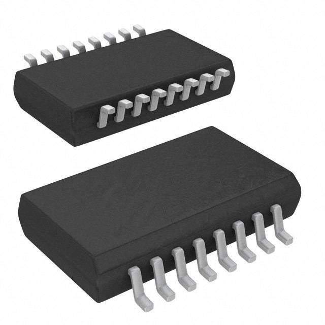
| 产品图片 |
|
| rohs | 否不符合限制有害物质指令(RoHS)规范要求 |
| 产品系列 | 放大器 IC,精密放大器,Analog Devices AD713JR-16- |
| 数据手册 | |
| 产品型号 | AD713JR-16 |
| 产品培训模块 | http://www.digikey.cn/PTM/IndividualPTM.page?site=cn&lang=zhs&ptm=30008http://www.digikey.cn/PTM/IndividualPTM.page?site=cn&lang=zhs&ptm=26202 |
| 产品种类 | 精密放大器 |
| 供应商器件封装 | 16-SOIC W |
| 共模抑制比—最小值 | 88 dB |
| 关闭 | No |
| 其它名称 | AD713JR16 |
| 包装 | 管件 |
| 压摆率 | 20 V/µs |
| 双重电源电压 | +/- 15 V |
| 商标 | Analog Devices |
| 增益带宽生成 | 4 MHz |
| 增益带宽积 | - |
| 安装类型 | 表面贴装 |
| 安装风格 | SMD/SMT |
| 封装 | Tube |
| 封装/外壳 | 16-SOIC(0.295",7.50mm 宽) |
| 封装/箱体 | SOIC-16 |
| 工作温度 | 0°C ~ 70°C |
| 工作电源电压 | 9 V to 36 V |
| 工厂包装数量 | 47 |
| 放大器类型 | J-FET |
| 最大双重电源电压 | +/- 18 V |
| 最大工作温度 | + 125 C |
| 最小双重电源电压 | +/- 4.5 V |
| 最小工作温度 | - 55 C |
| 标准包装 | 47 |
| 电压-电源,单/双 (±) | 9 V ~ 36 V, ±4.5 V ~ 18 V |
| 电压-输入失调 | 300µV |
| 电压增益dB | 112.04 dB |
| 电流-电源 | 10mA |
| 电流-输入偏置 | 55pA |
| 电流-输出/通道 | 25mA |
| 电源电压-最大 | 36 V |
| 电源电压-最小 | 9 V |
| 电源电流 | 12 mA |
| 电源类型 | Dual |
| 电路数 | 4 |
| 系列 | AD713 |
| 视频文件 | http://www.digikey.cn/classic/video.aspx?PlayerID=1364138032001&width=640&height=505&videoID=2245193153001http://www.digikey.cn/classic/video.aspx?PlayerID=1364138032001&width=640&height=505&videoID=2245193159001 |
| 转换速度 | 20 V/us at +/- 15 V |
| 输入偏压电流—最大 | 150 pA |
| 输入补偿电压 | 300 uV |
| 输出类型 | No |
| 通道数量 | 4 Channel |


- 商务部:美国ITC正式对集成电路等产品启动337调查
- 曝三星4nm工艺存在良率问题 高通将骁龙8 Gen1或转产台积电
- 太阳诱电将投资9.5亿元在常州建新厂生产MLCC 预计2023年完工
- 英特尔发布欧洲新工厂建设计划 深化IDM 2.0 战略
- 台积电先进制程称霸业界 有大客户加持明年业绩稳了
- 达到5530亿美元!SIA预计今年全球半导体销售额将创下新高
- 英特尔拟将自动驾驶子公司Mobileye上市 估值或超500亿美元
- 三星加码芯片和SET,合并消费电子和移动部门,撤换高东真等 CEO
- 三星电子宣布重大人事变动 还合并消费电子和移动部门
- 海关总署:前11个月进口集成电路产品价值2.52万亿元 增长14.8%


PDF Datasheet 数据手册内容提取
Precision, High Speed, BiFET Quad Op Amp AD713 FEATURES CONNECTION DIAGRAMS AC performance OUTPUT 1 14 OUTPUT 1 μs settling to 0.01% for 10 V step –IN 2 1 4 13 –IN 20 V/μs slew rate +IN 3 12 +IN AD713 0.0003% total harmonic distortion (THD) +VS 4 TOP VIEW 11 –VS 4 MHz unity gain bandwidth (Not to Scale) +IN 5 10 +IN DC performance –IN 6 2 3 9 –IN 18 .μ5V m/°VC mtyapxiicmalu dmri fotf fset voltage OUTPUT 7 8 OUTPUT 00824-001 Figure 1. 14-Lead PDIP (N) and CERDIP (Q) Packages 150 V/mV minimum open-loop gain 2 μV p-p typical noise, 0.1 Hz to 10 Hz True 14-bit accuracy OUTPUT 1 16 OUTPUT Single version: AD711, dual version: AD712 –IN 2 1 4 15 –IN Available in 16-lead SOIC, 14-lead PDIP and CERDIP +IN 3 14 +IN APPLICATIONS +VS 4 AD713 13 –VS Active filters +IN 5 12 +IN Quad output buffers for 12- and 14-bit DACs –IN 6 2 3 11 –IN Input buffers for precision ADCs OUTPUT 7 TOP VIEW 10 OUTPUT NC 8 (Not to Scale) 9 NC Photo diode preamplifier applications NCC =O NNON ECCOTNTNOE CTTH.I SD OP INNO.T 00824-002 Figure 2. 16-Lead SOIC_W (RW) Package GENERAL DESCRIPTION The AD713 is a quad operational amplifier, consisting of four PRODUCT HIGHLIGHTS AD711 BiFET op amps. These precision monolithic op amps 1. The AD713 is a high speed BiFET op amp that offers offer excellent dc characteristics plus rapid settling times, high excellent performance at competitive prices. It upgrades slew rates, and ample bandwidths. In addition, the AD713 provides the performance of circuits using op amps such as the the close matching ac and dc characteristics inherent to amplifiers TL074, TL084, LT1058, LF347, and OPA404. sharing the same monolithic die. The single-pole response of 2. Slew rate is 100% tested for a guaranteed minimum of the AD713 provides fast settling: l μs to 0.01%. This feature, 16 V/μs (J and A grades). combined with its high dc precision, makes the AD713 suitable 3. The combination of Analog Devices, Inc., advanced for use as a buffer amplifier for 12- or 14-bit DACs and ADCs. processing technology, laser wafer drift trimming, and It is also an excellent choice for use in active filters in 12-, 14- well-matched ion-implanted JFETs provides outstanding and 16-bit data acquisition systems. Furthermore, the AD713 dc precision. Input offset voltage, input bias current and low total harmonic distortion (THD) level of 0.0003% and very input offset current are specified in the warmed-up close matching ac characteristics make it an ideal amplifier for condition and are 100% tested. many demanding audio applications. The AD713 is internally 4. Very close matching of ac characteristics between the four compensated for stable operation at unity gain. The AD713J is amplifiers makes the AD713 ideal for high quality active rated over the commercial temperature range of 0°C to 70°C. filter applications. The AD713A is rated over the industrial temperature of −40°C to +85°C. The AD713 is offered in 16-lead SOIC, 14-lead PDIP, and 14-lead CERDIP packages. Rev. F Information furnished by Analog Devices is believed to be accurate and reliable. However, no responsibility is assumed by Analog Devices for its use, nor for any infringements of patents or other One Technology Way, P.O. Box 9106, Norwood, MA 02062-9106, U.S.A. rights of third parties that may result from its use. Specifications subject to change without notice. No license is granted by implication or otherwise under any patent or patent rights of Analog Devices. Tel: 781.329.4700 www.analog.com Trademarks and registered trademarks are the property of their respective owners. Fax: 781.461.3113 ©2002–2011 Analog Devices, Inc. All rights reserved.
AD713 TABLE OF CONTENTS Features..............................................................................................1 Theory of Operation......................................................................11 Applications.......................................................................................1 Measuring AD713 Settling Time.............................................11 Connection Diagrams......................................................................1 Power Supply Bypassing............................................................11 General Description.........................................................................1 A High Speed Instrumentation Amplifier Circuit.................12 Product Highlights...........................................................................1 A High Speed 4-Op-Amp Cascaded Amplifier Circuit........12 Revision History...............................................................................2 High Speed Op Amp Applications and Techniques..............12 Specifications.....................................................................................3 CMOS DAC Applications.........................................................14 Absolute Maximum Ratings............................................................5 Filter Applications......................................................................14 Thermal Resistance......................................................................5 GIC and FDNR Filter Applications.........................................15 ESD Caution..................................................................................5 Outline Dimensions.......................................................................17 Typical Performance Characteristics.............................................6 Ordering Guide..........................................................................18 Test Circuits.....................................................................................10 REVISION HISTORY 7/11—Rev. E to Rev. F Deleted Figure 9 and Figure 10; Renumbered Sequentially........9 Changes to Figure 23 Caption and Figure 24 Caption..............10 Changes to Figure 2..........................................................................1 Added Test Circuits Section..........................................................11 6/11—Rev. D to Rev. E Moved Figures 26, Figure 27, and Figure 28...............................11 Changed 8 μV/°C Maximum Drift to 8 μV/°C Typical Drift in Changes to Figure 29......................................................................12 Features Section................................................................................1 Changes to DAC Buffers (I-to-V Converters) Section..............13 Changes to Figure 37 and Table 5.................................................14 5/11—Rev. C to Rev. D Changed C1 to C ...........................................................................14 L Updated Format..................................................................Universal Changes to Figure 43 and Figure 44.............................................15 Changes to Features Section, General Description Section, and Updated Outline Dimensions.......................................................18 Product Highlights Section.............................................................1 Changes to Ordering Guide..........................................................19 Deleted S, K, B, and T Grades Throughout...................................1 10/01—Rev. B to Rev. C Changes to Table 1............................................................................3 Changes to Table 2............................................................................5 Edits to Features.................................................................................1 Added Typical Performance Characteristics Summary..............6 Edits to Product Description...........................................................1 Change to Figure 7...........................................................................7 Edits to Ordering Guide...................................................................3 Changes to Figure 15, Figure 17, and Figure 18...........................8 Edits to Metallization Photograph..................................................3 Rev. F | Page 2 of 20
AD713 SPECIFICATIONS V = ±15 V at T = 25°C, unless otherwise noted. S A Table 1. AD713J/AD713A Parameter Test Conditions/Comments Min Typ Max Unit INPUT OFFSET VOLTAGE1 Initial Offset 0.3 1.5 mV Offset T to T 0.5 2 mV MIN MAX vs. Temp 5 μV/°C vs. Supply 78 95 dB T to T 76 95 dB MIN MAX Long-Term Stability 15 μV/Month INPUT BIAS CURRENT2 V = 0 V 40 150 pA CM V = 0 V at T 3.4/9.6 nA CM MAX V = ±10 V 55 200 pA CM INPUT OFFSET CURRENT V = 0 V 10 75 pA CM V = 0 V at T 1.7/4.8 pA CM MAX MATCHING CHARACTERISTICS Input Offset Voltage 0.5 1.8 mV T to T 0.7 2.3 mV MIN MAX Input Offset Voltage Drift 8 μV/°C Input Bias Current 10 100 pA Crosstalk f = 1 kHz −130 dB f = 100 kHz −95 dB FREQUENCY RESPONSE Small Signal Bandwidth G = −1 3.0 4.0 MHz Full Power Response V = 20 V p-p 200 kHz O Slew Rate G = −1 16 20 V/μs Settling Time to 0.01% 1.0 1.2 μs Total Harmonic Distortion f = 1 kHz; R ≥ 2 kΩ; V = 3 V rms 0.0003 % L O INPUT IMPEDANCE Differential3 3 × 10¹²||5.5 Ω||pF Common Mode4 3 × 10¹²||5.5 Ω||pF INPUT VOLTAGE RANGE Differential ±20 V Common-Mode Voltage +14.5/−11.5 V T to T −11 +13 V MIN MAX Common Mode V = ±10 V 78 88 dB CM Rejection Ratio T to T 76 84 dB MIN MAX V = ±11 V 72 84 dB CM T to T 70 80 dB MIN MAX INPUT VOLTAGE NOISE 0.1 Hz to 10 Hz 2 μV p-p f = 10 Hz 45 nV/√Hz f = 100 Hz 22 nV/√Hz f = 1 kHz 18 nV/√Hz f = 10 kHz 16 nV/√Hz INPUT CURRENT NOISE f = 1 kHz 0.01 pA/√Hz OPEN-LOOP GAIN V = ±10 V; R ≥ 2 kΩ 150 400 V/mV O L T to T 100 V/mV MIN MAX Rev. F | Page 3 of 20
AD713 AD713J/AD713A Parameter Test Conditions/Comments Min Typ Max Unit OUTPUT CHARACTERISTICS Voltage R ≥ 2 kΩ +13/−12.5 +13.9/−13.3 V L T to T ±12 +13.8/−13.1 V MIN MAX Current Short circuit 25 mA POWER SUPPLY Rated Performance ±15 V Operating Range ±4.5 ±18 V Quiescent Current 10.0 13.5 mA TRANSISTOR COUNT Number of transistors 120 1 Input offset voltage specifications are guaranteed after 5 minutes of operation at TA = 25°C. 2 Bias current specifications are guaranteed maximum at either input after 5 minutes of operation at TA = 25°C. For higher temperatures, the current doubles every 10°C. 3 Defined as the voltage between inputs, such that neither exceeds ±10 V from ground. 4 Typically exceeding −14.1 V negative common-mode voltage on either input results in an output phase reversal. Rev. F | Page 4 of 20
AD713 ABSOLUTE MAXIMUM RATINGS Stresses above those listed under Absolute Maximum Ratings Table 2. may cause permanent damage to the device. This is a stress Parameter Rating rating only; functional operation of the device at these or any Supply Voltage ±18 V other conditions above those indicated in the operational Input Voltage1 ±18 V section of this specification is not implied. Exposure to absolute Output Short-Circuit Duration maximum rating conditions for extended periods may affect (For One Amplifier) Indefinite device reliability. Differential Input Voltage +V and −V S S Storage Temperature Range (Q) −65°C to +150°C THERMAL RESISTANCE Storage Temperature Range (N, R) −65°C to +125°C θ is specified for the worst-case conditions, that is, a device JA Operating Temperature Range soldered in a circuit board for surface-mount packages. AD713J 0°C to 70°C AD713A −40°C to +85°C Table 3. Thermal Resistance Lead Temperature Range (Soldering, 60 sec) 300°C Package Type θJA θ JC Unit 14-Lead PDIP (N-14) 100 30 °C/W 1 For supply voltages less than ±18 V, the absolute maximum input voltage is 14-Lead CERDIP (Q-14) 110 30 °C/W equal to the supply voltage. 16-Lead SOIC_W (RW-16) 100 30 °C/W ESD CAUTION Rev. F | Page 5 of 20
AD713 TYPICAL PERFORMANCE CHARACTERISTICS V = ±15 V at T = 25°C, unless otherwise noted. S A 20 16 RL = 2kΩ TA = 25°C V) 15 A) 12 WING ( NT (m E S RRE AG 10 CU 8 T VOLT SCENT U E INP 5 QUI 4 00 5 SUPPLY VO10LTAGE (±V) 15 2000824-003 00 5 SUPPLY V1O0LTAGE (V) 15 2000824-006 Figure 3. Input Voltage Swing vs. Supply Voltage Figure 6. Quiescent Current vs. Supply Voltage 20 10–6 RL = 2kΩ TA = 25°C 10–7 V) E SWING ( 15 +VOUT RENT (A) 10–8 G R TA 10 CU 10–9 PUT VOL –VOUT UT BIAS 10–10 UT 5 NP O I 10–11 00 5 SUPPLY VO10LTAGE (±V) 15 2000824-004 10–12–60 –40 –20 0 TEM20PERA4T0URE6 (0°C) 80 100 120 14000824-007 Figure 4. Output Voltage Swing vs. Supply Voltage Figure 7. Input Bias Current vs. Temperature 30 100 p) 25 p- WING (V 20 ±15V SUPPLIES NCE (Ω) 10 S A T VOLTAGE 1150 TPUT IMPED 1 U U TP O 0.1 U O 5 010 1L0O0AD RESISTANCE (1Ωk) 10k00824-005 0.011k 10k FREQU1E0N0kCY (Hz) 1M 10M00824-008 Figure 5. Output Voltage Swing vs. Load Resistance Figure 8. Output Impedance vs. Frequency, G = 1 Rev. F | Page 6 of 20
AD713 50 100 100 VS = ±15V TA = 25°C 80 80 40 RRENT (pA) 30 GAIN (dB) 60 60 N (Degrees) INPUT BIAS CU 20 OPEN-LOOP 4200 2PkHGΩA|A|S1INE00pF LOAD 4200 PHASE MARGI 10 0 0 0–10 –5COMMON-MOD0E VOLTAGE (V)5 1000824-009 –2010 100 1kFREQU1E0NkCY (Hz)100k 1M 10M–20 00824-012 Figure 9. Input Bias Current vs. Common Mode Voltage Figure 12. Open-Loop Gain and Phase Margin vs. Frequency 26 125 +OUTPUT CURRENT RL = 2kΩ mA) 24 120 TA = 25°C LIMIT ( 22 –OUTPUT CURRENT dB) 115 ENT 20 AIN ( R G CUR 18 OP 110 CIRCUIT 16 OPEN-LO 105 T 14 R HO 100 S 12 10–60 –40 –20 AM0BIEN2T0 TEM4P0ERA6T0URE 8(°0C) 100 120 14000824-010 950 5 SUPPLY V1O0LTAGE (V) 15 2000824-013 Figure 10. Short-Circuit Current Limit vs. Temperature Figure 13. Open-Loop Gain vs. Supply Voltage 5.0 110 100 +SUPPLY MHz) 4.5 N (dB) 80 DTH ( CTIO ANDWI 4.0 Y REJE 60 –SUPPLY B L AIN UPP 40 G S Y R NIT 3.5 WE U PO 20 VS = ±15V SUPPLIES WITH 1V p-p SINE WAVE 25°C 3.0–60 –40 –20 0 TE2M0PERA40TURE6 0(°C) 80 100 120 14000824-011 010 S10U0PPLY MOD1UkLATION FR10EkQUENCY 1(H00zk) 1M00824-014 Figure 11. Gain Bandwidth vs. Temperature Figure 14. Power Supply Rejection vs. Frequency Rev. F | Page 7 of 20
AD713 100 70 VS = ±15V 3V RMS VCM = 1V p-p RL = 2kΩ TA = 25°C 80 CL = 100pF 80 90 60 B) B) d d R ( D (100 M H C 40 T 110 20 120 010 100 FR1kEQUENCY 1(H0zk) 100k 1M00824-015 130100 1kFREQUENCY (Hz)10k 100k00824-018 Figure 15. Common-Mode Rejection vs. Frequency Figure 18. Total Harmonic Distortion vs. Frequency 30 1k RL = 2kΩ TA = 25°C 25 VS = ±15V Hz) E (V p-p) 20 GE (nV/100 G A A T LT 15 OL O V V E UTPUT 10 T NOIS 10 O U P N 5 I 1000k INPUT FRE1QMUENCY (Hz) 10M00824-016 11 10 F1R0E0QUENCY (1Hkz) 10k 100k00824-019 Figure 16. Large Signal Frequency Response Figure 19. Input Noise Voltage Spectral Density 10 25 S LT 8 O V ± 6 20 L A N 4 TO FI 2 V/µs) 15 M 0V 0 1% 0.1% 0.01% ATE ( O R G FR –2 ERROR 1% 0.1% 0.01% LEW 10 N S WI –4 S T –6 5 U P T U –8 O –100.5 0.6 SE0T.T7LING TIME0 .(8µs) 0.9 1.000824-017 00 100 200 IN(A3P0TU0 TS UEMR4MR00OINRG S J5IUG00NNCATLI6 O(0mN0V)) 700 800 90000824-020 Figure 17. Output Swing and Error vs. Settling Time Figure 20. Slew Rate vs. Input Error Signal Rev. F | Page 8 of 20
AD713 –70 –80 1 14 2 13 1 4 –90 3 12 1 TO 4 100•••• •••• •••• •••• •••• •••• •••• •••• •••• •••• B) 4 11 1 TO 2 90 K (d –100 5 2 3 10 1 TO 3 L 6 9 A ST 7 8 S –110 O R C –120 –130 10 0%•••• •••• •••• •••• •••• •••• •••• •••• •••• •••• –14010 100 FREQUE1NkCY (Hz) 10k 100k 00824-022 5V 1µs 00824-027 Figure 21. Crosstalk vs. Frequency (see Figure 26 for Test Circuit) Figure 24. Unity Gain Inverter Pulse Response—Small Signal (see Figure 28) 100•••• •••• •••• •••• •••• •••• •••• •••• •••• •••• 100•••• •••• •••• •••• •••• •••• •••• •••• •••• •••• 90 90 10 10 0%•••• •••• •••• •••• •••• •••• •••• •••• •••• •••• 0%•••• •••• •••• •••• •••• •••• •••• •••• •••• •••• 5V 1µs 00824-024 50mV 200ns 00824-028 Figure 22. Unity Gain Follower Pulse Response—Large Signal (see Figure 27 Figure 25. Unity Gain Inverter Pulse Response—Small Signal (see Figure 28) for Test Circuit) 100•••• •••• •••• •••• •••• •••• •••• •••• •••• •••• 90 10 0%•••• •••• •••• •••• •••• •••• •••• •••• •••• •••• 50mV 100ns 00824-026 Figure 23. Unity Gain Follower Pulse Response—Small Signal (see Figure 27) Rev. F | Page 9 of 20
AD713 TEST CIRCUITS 9kΩ 1kΩ +VS + APIDN7 143 +VS 0.1µF 1µF 1/4 AD713 OUTPUT COM + +1µF 0.1µF 0.1µF 1µF 4 GSRIINGOOPNURUANTLD* 1kΩ AAALRSL ES 4HC OOAMWNNPNEL.ICFTIEERDS –VS APIDN7 1131 VIN AD17/41131 2kRΩL 1C0LpF VOUT *TAAHMMEPP LLSIIIFFGIINEERRA SLA AITN RAPEU T TTIM H(1EEkN. HT MzH SEEIA NOSEUUWTRPAEUVDTE FS, O 2OVRF pC T-RpHO)E IS SOS ATTHPAPELLRKI .ETDH RTEOE ONE 00824-021 SIQWNUAPAVURETE –VS + 1µF 0.1µF 00824-023 Figure 26. Crosstalk Test Circuit for Figure 21 Figure 27. Unity Gain Follower Circuit for Figure 22 and Figure 23 7.5pF 2kΩ +VS VIN 2kΩ 4 +1µF 0.1µF 1/4 AD713 VOUT SQUARE RL CL WAVE 11 2kΩ 10pF INPUT –VS + 1µF 0.1µF 00824-025 Figure 28. Unity Gain Inverter Circuit for Figure 24 and Figure 25 Rev. F | Page 10 of 20
AD713 THEORY OF OPERATION MEASURING AD713 SETTLING TIME The error signal is thus clamped twice: once to prevent overload- ing amplifier A2 and then a second time to avoid overloading Figure 30 and Figure 31 show the dynamic response of the AD713 the oscilloscope preamp. A Tektronix oscilloscope preamp while operating in the settling time test circuit of Figure 29. Type 7A26 was carefully chosen because it recovers from the The input of the settling time fixture is driven by a flat-top pulse approximately 0.4 V overload quickly enough to allow accurate generator. The error signal output from the false summing node measurement of the AD713 1 μs settling time. Amplifier A2 is a of A1, the AD713 under test, is clamped, amplified by Op Amp very high speed FET input op amp; it provides a voltage gain of A2, and then clamped again. 10, amplifying the error signal output of the AD713 under test TO TEKTRONIX 7A26 (providing an overall gain of 5). OSCILLOSCOPE PREAMP INPUT SECTION (VIA LESS 1MΩ 20pF THAN 1FT 50Ω 5V COAXIAL CABLE) 5pF 100•••• •••• •••• •••• •••• •••• •••• •••• •••• •••• + VERROR × 5 90 2 × A2 HP2835 206Ω 2 × HP2835 0.47µF 0.47µF –VS +VS 10kΩ NOTES 10 1.1kΩ 1. USE CIRCUIT BOARD 0%•••• •••• •••• •••• •••• •••• •••• •••• •••• •••• WITH GROUND PLANE. 4.99kΩ0.2pFTO 0.8p4F.99kΩ 5mV 500ns 00824-031 200Ω 10kΩ Figure 31. Settling Characteristics to –10 V Step, FLAT-TOP 5pF TO 18pF Upper Trace: Output of AD713 Under Test (5 V/div), PULSE *USE VERY Lower Trace: Amplified Error Voltage (0.01%/div) GENERATOR VIN 10kΩ AD17/413 SOHRO TRETR CMAINBALTEION POWER SUPPLY BYPASSING * RESISTOR DATA A1 The power supply connections to the AD713 must maintain a DYNAMICS 4 5kΩ 10pF 5109 + 11 low impedance to ground over a bandwidth of 4 MHz or more. OR EQUIVALENT This is especially important when driving a significant resistive +1µF 0.1µF–VS +VS 1µF+ 0.1µF 00824-029 ocor mcaepsa fcriotmive t hloea pdo bweecra suuspep alilel sc. uMrruelntitp ldee hliivgehr eqdu atloit yth bey lpoaasds Figure 29. Settling Time Test Circuit capacitors are recommended for each power supply line in any critical application. As shown in Figure 32, a 0.1 μF ceramic and a 1 μF electrolytic capacitor placed as close as possible to the 5V amplifier (with short lead lengths to power supply common) assures adequate high frequency bypassing in most applications. 100•••• •••• •••• •••• •••• •••• •••• •••• •••• •••• A minimum bypass capacitance of 0.1 μF should be used for 90 any application. +VS + 1µF 0.1µF 4 1/4 AD713 11 10 0%•••• •••• •••• •••• •••• •••• •••• •••• •••• •••• 5mV 500ns 00824-030 Figure 32. Recomm–eVnSded +Pow1µeFr Sup0p.1lyµ FBy00824-032p assing Figure 30. Settling Characteristics 0 V to 10 V Step, Upper Trace: Output of AD713 Under Test (5 V/div), Lower Trace: Amplified Error Voltage (0.01%/div) Rev. F | Page 11 of 20
AD713 A HIGH SPEED INSTRUMENTATION AMPLIFIER A HIGH SPEED 4-OP-AMP CASCADED AMPLIFIER CIRCUIT CIRCUIT The instrumentation amplifier circuit shown in Figure 33 can Figure 35 shows how the four amplifiers of the AD713 can be provide a range of gains from unity up to 1000 and higher using connected in cascade to form a high gain, high bandwidth only a single AD713. The circuit bandwidth is 1.2 MHz at a gain amplifier. This gain of 100 amplifier has a −3 dB bandwidth of 1 and 250 kHz at a gain of 10; settling time for the entire greater than 600 kHz. circuit is less than 5 μs to within 0.01% for a 10 V step, (G = 10). +VS Other uses for Amplifier A4 include an active data guard and an 1µF 0.1µF active sense input. INPUT 3 4 20,000 1 5 1/4 AD17/413CIRCUIT GAIN = R G + 1 2 AD17/413 6 1/47 10 8 12 AD713 –IN 3 *1.5pFTO 20pF 2.15kΩ AD713 9 1/4 14 A1 1 (TRIM FOR BEST SETTLING TIME) 2.15kΩ AD713 13 11 OUTPUT 2 1kΩ 1kΩ 2.15kΩ 2.15kΩ 10kΩ 10kΩ** 1kΩ 1kΩ 22MΩ 1µF 0.1µF 7.5pF 10kΩ** 9 SENSE –VS +VS –VS + RG 7.5pF 150pkFΩ** 10 AA3D17/4183 OAPDTJIU1OS0N0TAkMΩLE VNOTS 4GB-AAONIPND- A=WM 1IDP00T CHA (S–C3dABD)E =D 6 A3M2kPHLzIFIER 00824-035 10kΩ** Figure 35. High Speed 4-Op-Amp Cascaded Amplifier Circuit 10kΩ 6 TO SPECTRUM ANALYZER A2 7 13 ERROR SIGNAL +IN 5 AD17/413 14 A4 12 TVROOEF LBETURAFEGFNEECREED NULL (EORURTOPRU/1T1) AD17/413 OR REMOTE 1kΩ ADJUST 10kΩ GROUND SENSE 100kΩ +VS 0.1µF +1µF APIDN7 143 *VOLTRONICS SP20 TRIMMER CAPACITOR +VS 10kΩ C–OVMS 0.1µF +1µF APIDN7 1131**ORRAERST EIISOQT UMOIAVRATSCLEHNETD 1% METAL FILM 00824-033 LSOINWE WDIASVTEO1 kIRNΩTPIUOTN AD17/4134 +1µF 0.1µF Figure 33. High Speed Instrumentation Amplifier Circuit 11 100pF Table 4 provides a performance summary for this circuit. Figure 34 shows the pulse response of this circuit for a gain of 10. –VS + 1µF 0.1µF 00824-036 Figure 36. THD Test Circuit Table 4. Performance Summary for the High Speed Instrumentation Amplifier Circuit HIGH SPEED OP AMP APPLICATIONS AND Gain R Bandwidth Settling Time (0.01%) TECHNIQUES G 1 NC1 1.2 MHz 2 μs DAC Buffers (I-to-V Converters) 2 20 kΩ 1.0 MHz 2 μs The wide input dynamic range of JFET amplifiers makes them 10 4.04 kΩ 0.25 MHz 2 μs ideal for use in both waveform reconstruction and digital audio 1 NC = no connect. DAC applications. The AD713, in conjunction with a 16-bit DAC, can achieve 0.0016% THD without requiring the use of a 5V deglitcher in digital audio applications. 100•••• •••• •••• •••• •••• •••• •••• •••• •••• •••• Driving the Analog Input of an Analog-to-Digital 90 Converter An op amp driving the analog input of an analog-to-digital converter (ADC), such as that shown in Figure 37, must be capable of maintaining a constant output voltage under dynami- cally changing load conditions. In successive approximation converters, the input current is compared to a series of switched 10 0%•••• •••• •••• •••• •••• •••• •••• •••• •••• •••• trial currents. The comparison point is diode clamped but may 2µs 00824-034 vmaoryd ublya tsieovne roafl thhuen adnraeldo gm-tioll-idvoigltitsa, lr einsupulttin cgu rinre hnitg. hT hfree qouuetpnucty Figure 34. Pulse Response of High Speed Instrumentation Amplifier, impedance of a feedback amplifier is made artificially low by its Gain = 10 Rev. F | Page 12 of 20
AD713 loop gain. At high frequencies, where the loop gain is low, the 1mV AD713 BUFF amplifier output impedance can approach its open-loop value. 100•••• •••• •••• •••• •••• •••• •••• •••• •••• •••• 1 VLOGIC STS 28 90 2 12/8 (MSB) DB11 27 3 CS DB10 26 HIGH AD574A 4 AO DB9 25 BITS TOP VIEW 5 R/C DB8 24 (Notto Scale) 6 CE DB7 23 7 VCC DB6 22 MIDDLE 8 REF OUT DB5 21 BITS GAINADJUST 9 AC DB4 20 10 10 REF IN DB3 19 ±10V +145V0.1µF OFFSRE1T R1A20 D01ΩJ0U0ΩST 11111234 VB1200EIPVVE IIONNFF(LSB) DDDDBBBC021 11117685 LBOITWS 0%•••F•igu••re• •39•. •B•u•ffe•r•5 R•0e•0cmo•V•v•e•ry •T•i–m•5•Ve S•Ai•Dn•Ck• ICN•u•r•re•n•t •=2• 01•0 mn•s•A• • 00824-041 ANIANLPOUGT 110.1µF ANALOG COM Driving A Large Capacitive Load 1A/D4713–15V 00824-039 The circuit of Figure 40 uses a 100 Ω isolation resistor that Figure 37. AD713 as an ADC Buffer enables the amplifier to drive capacitive loads exceeding 1500 pF; the resistor effectively isolates the high frequency Most IC amplifiers exhibit a minimum open-loop output imped- feedback from the load and stabilizes the circuit. Low frequency ance of 25 Ω, due to current limiting resistors. A few hundred feedback is returned to the amplifier summing junction via the microamps reflected from the change in converter loading can low-pass filter formed by the 100 Ω series resistor and the load introduce errors in instantaneous input voltage. If the analog- capacitance, C. Figure 41 shows a typical transient response for to-digital conversion speed is not excessive and the bandwidth L this connection. of the amplifier is sufficient, the amplifier output returns to the nominal value before the converter makes its comparison. 4.99kΩ However, many amplifiers have relatively narrow bandwidths, 30pF yielding slow recovery from output transients. The AD713 is +VS ideally suited as a driver for ADCs because it offers both a wide 0.1µF 4.99kΩ bandwidth and a high open-loop gain. 4 INPUT 1/4 100Ω OUTPUT TYPICAL CAPACITANCE AD713 1mV AD713 BUFF LIMIT FORVARIOUS 11 0.1µF CL RL LOAD RESISTORS 100•••• •••• •••• •••• •••• •••• •••• •••• •••• •••• RL CLUP TO 90 212k00kkΩΩΩ 111550000000pppFFF –VS 00824-042 Figure 40. Circuit for Driving a Large Capacitance Load 5V 1µs 100•••• •••• •••• •••• •••• •••• •••• •••• •••• •••• 10 90 0%•••• •••• •••• •••• •••• •••• •••• •••• •••• •••• 500mV 10V ADC IN 200ns 00824-040 Figure 38. Buffer Recovery Time Source Current = 2 mA 10 0%•••• •••• •••• •••• •••• •••• •••• •••• •••• •••• 00824-043 Figure 41. Transient Response, RL = 2 kΩ, CL = 500 pF Rev. F | Page 13 of 20
AD713 CMOS DAC APPLICATIONS VDD R2* C1 +15V The AD713 is an excellent output amplifier for CMOS DACs. It GAIN 33pF 0.1µF 18 20 can be used to perform both two- and four-quadrant operation. ADJUST VDD RFB The output impedance of a DAC using an inverted R-2R ladder VIN 19 VREF OUT1 1 1/4 4 approaches R for codes containing many 1s, 3R for codes R1* AD7545 AD713 VOUT containing a single 1, and infinity for codes containing all 0s. DGND AGND 2 11 0.1µF 3 ANALOG For example, the output resistance of the AD7545 modulates bfeeetdwbeaecnk 1r1e skisΩta anncde o3f3 1 k1Ω k.Ω T,h tehree fnoories,e w giathin t hvaer DieAs Cfr’os min t2e rton al *REFER TO TADBBL11E T5O. DB0 COMMON –15V 00824-044 4/3. This changing noise gain modulates the effect of the input Figure 42. Unipolar Binary Operation offset voltage of the amplifier, resulting in nonlinear DAC FILTER APPLICATIONS amplifier performance. The AD713, with its guaranteed 1.5 mV A Programmable State Variable Filter input offset voltage, minimizes this effect, achieving 12-bit For the state variable or universal filter configuration of Figure 44 performance. to function properly, DAC A1 and DAC B1 must control the Figure 42 and Figure 43 show the AD713 and a 12-bit CMOS gain and Q of the filter characteristic, and DAC A2 and DAC B2 DAC, the AD7545, configured for either a unipolar binary (two- must accurately track for the simple expression of f to be true. C quadrant multiplication) or bipolar (four-quadrant multiplication) This is readily accomplished using two AD7528 DACs and one operation. Capacitor C1 provides phase compensation, which AD713 quad op amp. Capacitor C3 compensates for the effects reduces overshoot and ringing. of op amp gain bandwidth limitations. Table 5. Recommended Trim Resistor Values vs. Grades for This filter provides low-pass, high-pass, and band-pass outputs AD7545 for V = 5 V and is ideally suited for applications where microprocessor D Trim Resistor JN/AQ KN/BQ LN/CQ GLN/GCQ control of filter parameters is required. The programmable R1 500 Ω 200 Ω 100 Ω 20 Ω range for component values shown is fC = 0 kHz to 15 kHz and R2 150 Ω 68 Ω 33 Ω 6.8 Ω Q = 0.3 to 4.5. VDD R2* R4 +15V 20kΩ R5 C1 1% 20kΩ GAIN 18 20 33pF 0.1µF 1% ADJUST VDD RFB R3 VIN 19 VREF OUT1 1 1/4 4 110%kΩ R1* AD7545 AD713 1/4 DGND AGND 2 AD713 VOUT 3 11 0.1µF 12 *REFER TO TABLE 5. DDBA1T1A T ION PDUBT0 CAONMALMOOGN –15V 00824-045 Figure 43. Bipolar Operation Rev. F | Page 14 of 20
AD713 R5 30kΩ +VS 1µF R4 C1 C2 CIRCUIT EQUATIONS 30kΩ C3 1000pF 1000pF + 33pF 2 4 10Rk3Ω C1 = C2, R1 = R2, R4 = R5 A1 1 6 HIGH 9 13 3 A2 7 PASS A3 8 A4 14 LOW PASS AD17/413 5 1/4 OUTPUT 10 1/4 12 11 AD17/413 OUTPUT fC =2π R11 C1 AD713 AD713 + VDD 2 20 19 18 VDD 4 2 18 20 –VS1µF Q = RR 34 ×RFRBFB1 VIN 147 ADDA7C5 2A81 DAC B1 1 17 DAC A2 AD7528 DAC B2 1 BOAUNTDPU PTASS AO = –RRSF RS RF 5 R1 R2 5 14 7 15 16 6 14 7 15 16 6 DAC EQUIVALENT RESISTANCE EQUALS DB0 TO DB0 TO DADTBA7 1 CS WR DDAACC BA/ DADTBA7 2 CS WR DDAACC AB/ 256 × (DDAACC L DAIDGDITEARL R CEOSDISETANCE) 00824-046 Figure 44. A Programmable State Variable Filter Circuit GIC AND FDNR FILTER APPLICATIONS 0 m) B The closely matched and uniform ac characteristics of the AD713 –10 E (d 0 make it ideal for use in generalized impedance converter (GIC)/ UD–1 m) T gyrator and frequency dependent negative resistor (FDNR) B –20 LI–2 filter applications. Figure 47 and Figure 48 show the AD713 E (d AMP–3 used in two typical active filters. The first shows a single AD713 LITUD –30 TPUT –4 simulating two coupled inductors configured as a one-third AMP –40 OU–5 16 18 20 22 24 octave band-pass filter. A single section of this filter meets T FREQUENCY (MHz) U ANSI Class II specifications and handles a 7.07 V rms signal TP –50 U with <0.002% THD (20 Hz to 20 kHz). O –60 Figure 48 shows a seven-pole antialiasing filter for a 2× over- s<2a00m .k0pH5l izdn,B ga np(8da8s hs.2-ab nkadHnledzs) r daip i5gp iVltea lar mnaudsd 1siio9g. n8ap aμpl s(l iV±c a0 t=.i3o ± nμ1.s 5 Td hVeil)sa ywf,i liattteh rd nhco at os –700 10 20 30 FR4E0QUE5N0CY (M60Hz) 70 80 90 10000824-048 S Figure 45. Output Amplitude vs. Frequency of 1/3 Octave Filter overload at any internal nodes. 3 OUTPUTAMPLITUDE The filter of Figure 47 can be scaled for any center frequency by 2 0 using the following formula: dB 1 –10 0 1.11 B) –20 –1 fC =2πRC DE (d –30 18 200 500 G1kROU2kP DEL5AkY10k 20k TU –40 19 where all resistors and capacitors scale equally. Resistors R3 to PLI µs20 R8 should not be greater than 2 kΩ in value to prevent parasitic AM –50 21 oscillations caused by the amplifier’s input capacitance. PUT –60 22 200 500 1k 2k 5k 10k 20k T –70 U If this is not practical, add small lead capacitances (10 pF to E O –80 V 20 pF) across R5 and R6. Figure 45 and Figure 46 show the TI –90 A output amplitude vs. frequency of these filters. EL–100 R –110 –12010k FREQUE10N0CkY (MHz) 1M 00824-049 Figure 46. Relative Output Amplitude vs. Frequency of Antialiasing Filter Rev. F | Page 15 of 20
AD713 R1 6.19kΩ INPUT OUTPUT C2 C2 R2 6800pF 6800pF 6.19kΩ R3 R4 1300Ω 1300Ω 5 12 R13500Ω AD17/413 7 R13600Ω AD17/413 14 2 6 9 13 1/4 R7 1/4 R8 1 AD713 1300Ω 8 AD713 1300Ω fC =21π.1R1C 3 C3 10 C4 6800pF 6800pF C1 = C2 = C3 = C4 = C R9 R11 R10 1300Ω 5.62kΩ 1300Ω RR111 = = R 42. 3=2 4Ω.76Ω +VS 0.1µF +1µF APIDN7 143 R3 = R4 = R5 = R6 = R7 = R8 = R9 = R10 = R COM + –VS 0.1µF 1µF APIDN7 1131 00824-047 Figure 47. A 1/3 Octave Filter Circuit 1/4 95.3kΩ AD713 1/4 2 412Ω 1.74kΩ 1.74kΩ 330Ω AD713 A1 1 12 INPUT 3 4700pF 100kΩ 4700pF B4 14 OUTPUT 10kΩ 36Ω 120Ω 130Ω 13 1kΩ 4700pF 4700pF 4700pF 1kΩ 10 3 10 1kΩ A3 8 1kΩ B1 1 1kΩ B3 8 6 9 13 2 6 9 7 A2 1kΩ AD17/413 14 A4 1kΩ AD17/413 7 B2 1kΩ AD17/413 5 12 5 1/4 1/4 1/4 AD713 1.2kΩ AD713 1.87kΩ AD713 1.1kΩ +VS + APIDN7 413 4700pF 4700pF 4700pF 0.1µF 1µF COM + –VS 0.1µF 1µF APIDN7 1113 00824-050 Figure 48. An Antialiasing Filter Rev. F | Page 16 of 20
AD713 OUTLINE DIMENSIONS 0.775 (19.69) 0.750 (19.05) 0.735 (18.67) 14 8 0.280 (7.11) 0.250 (6.35) 1 7 0.240 (6.10) 0.325 (8.26) 0.310 (7.87) 0.100 (2.54) 0.300 (7.62) BSC 0.060 (1.52) 0.195 (4.95) 0.210 (5.33) MAX 0.130 (3.30) MAX 0.115 (2.92) 0.015 0.150 (3.81) (0.38) 0.015 (0.38) 0.130 (3.30) MIN GAUGE 0.110 (2.79) SEATING PLANE 0.014 (0.36) PLANE 0.010 (0.25) 0.022 (0.56) 0.008 (0.20) 0.005 (0.13) 0.430 (10.92) 0.018 (0.46) MIN MAX 0.014 (0.36) 0.070 (1.78) 0.050 (1.27) 0.045 (1.14) COMPLIANTTO JEDEC STANDARDS MS-001 CONTROLLING DIMENSIONSARE IN INCHES; MILLIMETER DIMENSIONS (RCINOEFRPEANREREREN NLCTEEHA EODSNSEL MSY)AAAYNR BDEE AR CROOEU NNNFODIGETUDAR-POEPFDRFOA INSPC RWHIAH ETOEQL UFEIO VORAR LU EHSNAETL ISFN FLDOEEARSDIGSN.. 070606-A Figure 49. 14-Lead Plastic Dual In-Line Package [PDIP] Narrow Body (N-14) Dimensions shown in inches and (millimeters) 0.005 (0.13) MIN 0.098 (2.49) MAX 14 8 0.310 (7.87) 0.220 (5.59) 1 7 PIN 1 0.100 (2.54) BSC 0.320 (8.13) 0.290 (7.37) 0.785 (19.94) MAX 0.060 (1.52) 0.200 (5.08) 0.015 (0.38) MAX 0.150 0.200 (5.08) (3.81) 0.125 (3.18) MIN SEATING 0.015 (0.38) 0.023 (0.58) 0.070 (1.78) PLANE 15° 0.008 (0.20) 0.014 (0.36) 0.030 (0.76) 0° CONTROLLING DIMENSIONS ARE IN INCHES; MILLIMETER DIMENSIONS (IN PARENTHESES) ARE ROUNDED-OFF INCH EQUIVALENTS FOR REFERENCE ONLY AND ARE NOT APPROPRIATE FOR USE IN DESIGN. Figure 50. 14-Lead Ceramic Dual In-Line Package [CERDIP] (Q-14) Dimensions shown in inches and (millimeters) Rev. F | Page 17 of 20
AD713 10.50(0.4134) 10.10(0.3976) 16 9 7.60(0.2992) 7.40(0.2913) 1 10.65(0.4193) 8 10.00(0.3937) 1.27(0.0500) 0.75(0.0295) BSC 2.65(0.1043) 0.25(0.0098) 45° 0.30(0.0118) 2.35(0.0925) 8° 0.10(0.0039) 0° COPLANARITY 0.10 0.51(0.0201) SPLEAATNIENG 0.33(0.0130) 1.27(0.0500) 0.31(0.0122) 0.20(0.0079) 0.40(0.0157) C(RINOEFNPEATRRREOENNLCLTEIHNCEOGOSNDMELISPYM)LAEAIANNRNDSETIAORTRNOOESUJNANEORDDETEEDAICN-POSMPFTRIFALONLMPIDMIRLAELIRATIMTDEEESRTFSMEO;SRIRN-0ECU1QH3SU-EADIVAIINMAELDENENSSTIIOGSNNFS.OR 03-27-2007-B Figure 51. 16-Lead Standard Small Outline Package [SOIC_W] Wide Body (RW-16) Dimensions shown in millimeters and (inches) ORDERING GUIDE Model1 Temperature Range Package Description Package Option AD713AQ −40°C to +85°C 14-Lead CERDIP Q-14 AD713JNZ 0°C to 70°C 14-Lead PDIP N-14 AD713JR-16 0°C to 70°C 16-Lead SOIC_W RW-16 AD713JR-16-REEL 0°C to 70°C 16-Lead SOIC_W RW-16 AD713JR-16-REEL7 0°C to 70°C 16-Lead SOIC_W RW-16 AD713JRZ-16 0°C to 70°C 16-Lead SOIC_W RW-16 AD713JRZ-16-REEL 0°C to 70°C 16-Lead SOIC_W RW-16 AD713JRZ-16-REEL7 0°C to 70°C 16-Lead SOIC_W RW-16 1 Z = RoHS Compliant Part. Rev. F | Page 18 of 20
AD713 NOTES Rev. F | Page 19 of 20
AD713 NOTES ©2002–2011 Analog Devices, Inc. All rights reserved. Trademarks and registered trademarks are the property of their respective owners. D00824-0-7/11(F) Rev. F | Page 20 of 20