ICGOO在线商城 > 集成电路(IC) > 线性 - 放大器 - 仪表,运算放大器,缓冲器放大器 > AD648JRZ

 Datasheet下载
- 型号: AD648JRZ
- 制造商: Analog
- 库位|库存: xxxx|xxxx
- 要求:
| 数量阶梯 | 香港交货 | 国内含税 |
| +xxxx | $xxxx | ¥xxxx |
查看当月历史价格
查看今年历史价格
AD648JRZ产品简介:
ICGOO电子元器件商城为您提供AD648JRZ由Analog设计生产,在icgoo商城现货销售,并且可以通过原厂、代理商等渠道进行代购。 AD648JRZ价格参考。AnalogAD648JRZ封装/规格:线性 - 放大器 - 仪表,运算放大器,缓冲器放大器, J-FET 放大器 2 电路 8-SOIC。您可以下载AD648JRZ参考资料、Datasheet数据手册功能说明书,资料中有AD648JRZ 详细功能的应用电路图电压和使用方法及教程。
| 参数 | 数值 |
| -3db带宽 | - |
| 产品目录 | 集成电路 (IC)半导体 |
| 描述 | IC OPAMP JFET 1MHZ 8SOIC运算放大器 - 运放 LOW POWER DUAL IC |
| 产品分类 | Linear - Amplifiers - Instrumentation, OP Amps, Buffer Amps集成电路 - IC |
| 品牌 | Analog Devices Inc |
| 产品手册 | |
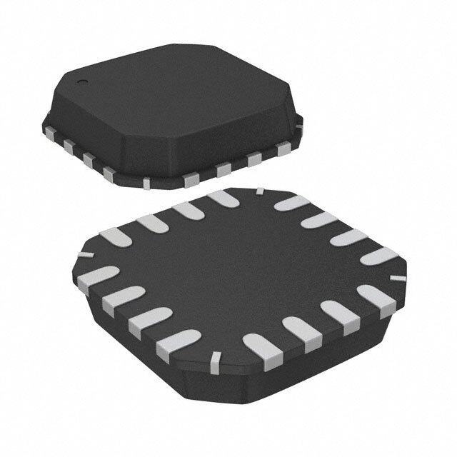
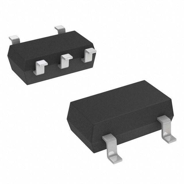
| 产品图片 |
|
| rohs | 符合RoHS无铅 / 符合限制有害物质指令(RoHS)规范要求 |
| 产品系列 | 放大器 IC,运算放大器 - 运放,Analog Devices AD648JRZ- |
| 数据手册 | |
| 产品型号 | AD648JRZ |
| 产品培训模块 | http://www.digikey.cn/PTM/IndividualPTM.page?site=cn&lang=zhs&ptm=30008http://www.digikey.cn/PTM/IndividualPTM.page?site=cn&lang=zhs&ptm=26202 |
| 产品目录页面 | |
| 产品种类 | 运算放大器 - 运放 |
| 供应商器件封装 | 8-SOIC |
| 共模抑制比—最小值 | 76 dB |
| 关闭 | No Shutdown |
| 包装 | 管件 |
| 压摆率 | 1.8 V/µs |
| 双重电源电压 | +/- 15 V |
| 商标 | Analog Devices |
| 增益带宽生成 | 1 MHz |
| 增益带宽积 | 1MHz |
| 安装类型 | 表面贴装 |
| 安装风格 | SMD/SMT |
| 封装 | Tube |
| 封装/外壳 | 8-SOIC(0.154",3.90mm 宽) |
| 封装/箱体 | SOIC-8 |
| 工作温度 | 0°C ~ 70°C |
| 工厂包装数量 | 98 |
| 技术 | FET |
| 放大器类型 | J-FET |
| 最大双重电源电压 | +/- 18 V |
| 最大工作温度 | + 70 C |
| 最小双重电源电压 | +/- 4.5 V |
| 最小工作温度 | 0 C |
| 标准包装 | 98 |
| 电压-电源,单/双 (±) | ±4.5 V ~ 18 V |
| 电压-输入失调 | 750µV |
| 电流-电源 | 340µA |
| 电流-输入偏置 | 5pA |
| 电流-输出/通道 | 15mA |
| 电路数 | 2 |
| 系列 | AD648 |
| 视频文件 | http://www.digikey.cn/classic/video.aspx?PlayerID=1364138032001&width=640&height=505&videoID=2245193153001http://www.digikey.cn/classic/video.aspx?PlayerID=1364138032001&width=640&height=505&videoID=2245193159001 |
| 转换速度 | 1.8 V/us |
| 输入偏压电流—最大 | 30 pA |
| 输入参考电压噪声 | 30 nV |
| 输入补偿电压 | 750 uV |
| 输出电流 | 2.4 mA |
| 输出类型 | - |
| 通道数量 | 2 Channel |


- 商务部:美国ITC正式对集成电路等产品启动337调查
- 曝三星4nm工艺存在良率问题 高通将骁龙8 Gen1或转产台积电
- 太阳诱电将投资9.5亿元在常州建新厂生产MLCC 预计2023年完工
- 英特尔发布欧洲新工厂建设计划 深化IDM 2.0 战略
- 台积电先进制程称霸业界 有大客户加持明年业绩稳了
- 达到5530亿美元!SIA预计今年全球半导体销售额将创下新高
- 英特尔拟将自动驾驶子公司Mobileye上市 估值或超500亿美元
- 三星加码芯片和SET,合并消费电子和移动部门,撤换高东真等 CEO
- 三星电子宣布重大人事变动 还合并消费电子和移动部门
- 海关总署:前11个月进口集成电路产品价值2.52万亿元 增长14.8%


PDF Datasheet 数据手册内容提取
a Dual Precision, Low Power BiFET Op Amp AD648 FEATURES CONNECTION DIAGRAM DC Performance 400 (cid:1)A max Quiescent Current Plastic Mini-Dip (N) Package, 10 pA max Bias Current, Warmed Up (AD648B) Plastic SOIC (R) Package 1 (cid:1)V max Offset Voltage (AD648B) and 10 (cid:1)V/(cid:2)C max Drift (AD648B) CERDIP (Q) Package 2 (cid:1)V p-p Noise, 0.1 Hz to 10 Hz AC Performance 1.8 V/(cid:1)s Slew Rate 1 MHz Unity Gain Bandwidth Available in Plastic Mini-DIP, CERDIP, and Plastic SOIC Packages MIL-STD-883B Parts Available Surface Mount (SOIC) Package Available in Tape and Reel in Accordance with EIA-481A Standard Single Version: AD548 PRODUCT DESCRIPTION –55°C to +125°C and the AD648T* grade is available pro- The AD648 is a matched pair of low power, precision mono- cessed to MIL-STD-883B, Rev. C. lithic operational amplifiers. It offers both low bias current The AD648 is available in an 8-lead plastic mini-DIP, (10 pA max, warmed up) and low quiescent current (400 µA CERDIP, and SOIC. max) and is fabricated with ion-implanted FET and laser wafer trimming technologies. Input bias current is guaranteed over the *Not for new design, obsolete April 2002. AD648’s entire common-mode voltage range. PRODUCT HIGHLIGHTS The economical J grade has a maximum guaranteed offset 1. A combination of low supply current, excellent dc and ac voltage of less than 2 mV and an offset voltage drift of less than performance and low drift makes the AD648 the ideal op 20 µV/°C. This level of dc precision is achieved using Analog’s amp for high performance, low power applications. laser wafer drift trimming process. The combination of low quiescent current and low offset voltage drift minimizes changes 2. The AD648 is pin compatible with industry standard dual in input offset voltage due to self-heating effects. Five grades are op amps such as the LF442, TL062, and AD642, enabling offered over the commercial, industrial and military temperature designers to improve performance while achieving a reduc- ranges. tion in power dissipation of up to 85%. The AD648 is recommended for any dual supply op amp 3. Guaranteed low input offset voltage (2 mV max) and drift application requiring low power and excellent dc and ac per- (20 µV/°C max) for the AD648J are achieved using Analog formance. In applications such as battery-powered, precision Devices’ laser drift trimming technology. instrument front ends and CMOS DAC buffers, the AD648’s 4. Analog Devices specifies each device in the warmed-up excellent combination of low input offset voltage and drift, low condition, insuring that the device will meet its published bias current, and low 1/f noise reduces output errors. High specifications in actual use. common-mode rejection (82 dB, min on the “B” grade) and 5. Matching characteristics are excellent for all grades. The high open-loop gain ensures better than 12-bit linearity in high input offset voltage matching between amplifiers in the impedance, buffer applications. AD648J is within 2 mV. The AD648 is pinned out in a standard dual op amp configura- 6. Crosstalk between amplifiers is less than –120 dB at 1 kHz. tion and is available in seven performance grades. The AD648J and AD648K are rated over the commercial temperature range of 0°C to 70°C. The AD648 and AD648B are rated over the industrial temperature range of –40°C to +85°C. The AD648S and AD648T are rated over the military temperature range of REV.E Information furnished by Analog Devices is believed to be accurate and reliable. However, no responsibility is assumed by Analog Devices for its use, nor for any infringements of patents or other rights of third parties that One Technology Way, P.O. Box 9106, Norwood, MA 02062-9106, U.S.A. may result from its use. No license is granted by implication or otherwise Tel: 781/329-4700www.analog.com under any patent or patent rights of Analog Devices. Fax: 781/326-8703 © Analog Devices, Inc., 2002
AD648–SPECIFICATIONS (@ + 25(cid:2)C and V = (cid:3)15 V dc, unless otherwise noted.) S AD648J/A/S AD648K/B/T Model Min Typ Max Min Typ Max Unit INPUT OFFSET VOLTAGE1 Initial Offset 0.75 2.0 0.3 1.0 T to T 3.0/3.0/3.0 1.5/1.5/2.0 mV MIN MAX vs. Temperature 20 10 µV/°C vs. Supply 80 86 dB vs. Supply, T to T 76/76/76 80 dB MIN MAX Long-Term Offset Stability 15 15 µV/month INPUT BIAS CURREN Either Input,2 V = 0 5 20 3 10 pA CM Either Input2 at T , V = 0 0.45/1.3/20 0.25/0.65/10 nA MAX CM Max Input Bias Current Over Common-Mode Voltage Range 30 15 pA Offset Current, V = 0 5 10 2 5 pA CM Offset Current at T 0.25/0.7/10 0.15/0.35/5 nA MAX MATCHING CHARACTERISTICS3 Input Offset Voltage 1.0 2.0 0.5 1.0 mV Input Offset Voltage T to T 3.0/3.0/3.0 1.5/1.5/2.0 mV MIN MAX Input Offset Voltage vs. Temperature 8 5 µV/°C Input Bias Current 10 5 pA Crosstalk –120 –120 dB INPUT IMPEDANCE Differential 1 × 101 2(cid:1)3 1 × 10¹²(cid:1)3 Ω(cid:1)pF Common Mode 3 × 10¹²(cid:1)3 3 × 10¹²(cid:1)3 Ω(cid:1)pF INPUT VOLTAGE RANGE Differential4 ±20 ±20 V Common Mode ±11 ±12 ±11 ±12 V Common-Mode Rejection V = ±10 V 76 82 dB CM T to T 76/76/76 82 dB MIN MAX V = ±11 V 70 76 dB CM T to T 70/70/70 76 dB MIN MAX INPUT VOLTAGE NOISE Voltage 0.1 Hz to 10 Hz 2 2 µV p-p f = 10 Hz 80 80 nV/√Hz f = 100 Hz 40 40 nV/√Hz f = 1 kHz 30 30 nV/√Hz f = 10 kHz 30 30 nV/√Hz INPUT CURRENT NOISE f = 1 kHz 1.8 1.8 fA/√Hz FREQUENCY RESPONSE Unity Gain, Small Signal 0.8 1.0 0.8 1.0 MHz Full Power Response 30 30 kHz Slew Rate, Unity Gain 1.0 1.8 1.0 1.8 V/µs Settling Time to ±0.01% 8 8 µs OPEN-LOOP GAIN V = ±10 V, R ≥ 10 kΩ 300 1000 300 1000 V/mV O L T to T , R ≥ 10 kΩ 300/300/300 700 300 700 V/mV MIN MAX L V = ±10 V, R ≥ 5 kΩ 150 500 150 500 V/mV O L T to T , R ≥ 5 kΩ 150/150/150 300 150 300 V/mV MIN MAX L –2– REV. E
AD648 SPECIFICATIONS (Continued) AD648J/A/S AD648K/B/T Model Min Typ Max Min Typ Max Unit OUTPUT CHARACTERISTICS Voltage @ R ≥ 10 kΩ, L T to T ±12/±12/±12 ±13 ±12 ±13 V MIN MAX Voltage @ R ≥ 5 kΩ, L T to T ±11/±11/±11 ±12 ±11 ±12 V MIN MAX Short Circuit Current 15 15 mA POWER SUPPLY Rated Performance ±15 ±15 V Operating Range ±4.5 ±18 ±4.5 ±18 V Quiescent Current (Both Amplifiers) 340 400 340 400 µA TEMPERATURE RANGE Operating, Rated Performance Commercial (0°C to 70°C) AD648J AD648K Industrial (–40°C to +85°C) AD648A AD648B Military (–55°C to +125°C) AD648S AD648T PACKAGE OPTIONS SOIC (R-8) AD648JR AD648KR Plastic (N-8) AD648JN AD648KN CERDIP (Q-8) AD648AQ5, AD648SQ5 AD648BQ5, AD648TQ/883B5 Tape and Reel AD648JR-REEL, AD648JR-REEL7 AD648KR-REEL, AD648KR-REEL7 NOTES 1Input Offset Voltage specifications are guaranteed after five minutes of operation at T = 25°C. A 2Bias Current specifications are guaranteed maximum at either input after five minutes of operation at T = 25°C. For higher temperature, the current doubles A every 10°C. 3Matching is defined as the difference between parameters of the two amplifiers. 4Defined as voltages between inputs, such that neither exceeds ±10 V from ground. 5Not for new design. Obsolete April 2002. Specifications subject to change without notice. REV. E –3–
AD648 ABSOLUTE MAXIMUM RATINGS1 SupplyVoltage . . . . . . . . . . . . . . . . . . . . . . . . . . . . . . . . .±18V InternalPowerDissipation2 . . . . . . . . . . . . . . . . . . . .500 mW Input Voltage3 . . . . . . . . . . . . . . . . . . . . . . . . . . . . . . . . ±18 V Output Short Circuit Duration . . . . . . . . . . . . . . . . .Indefinite DifferentialInputVoltage . . . . . . . . . . . . . . . . . . +V and –V S S Storage Temperature Range (Q, H) . . . . . . .–65°C to +150°C Storage Temperature Range (N, R) . . . . . . . .–65°C to +125°C Operating Temperature Range AD648J/K . . . . . . . . . . . . . . . . . . . . . . . . . . . . .0°C to 70°C AD648A/B . . . . . . . . . . . . . . . . . . . . . . . . . .–40°C to +85°C AD648S/T . . . . . . . . . . . . . . . . . . . . . . . . .–55°C to +125°C Lead Temperature Range (Soldering60sec) . . . . . . . . . 300°C NOTES 1Stresses above those listed under “Absolute Maximum Ratings” may cause permanent damage to the device. This is a stress rating only and functional operation of the device at these or any other conditions above those indicated in the operational section of this specification is not implied. Exposure to absolute maximum rating conditions for extended periods may affect device reliability. 2Thermal Characteristics: 8-Pin Plastic Package: θ = 165°C/Watt JA 8-Pin CERDIP Package: θ = 22°C/Watt; θ = 110°C/Watt JC JA 8-Pin SOIC Package: θ = 42°C/Wat; θ = 160°C/Watt JC JA 3For supply voltages less than ±18 V, the absolute maximum input voltage is equal to the supply voltage. CAUTION ESD (electrostatic discharge) sensitive device. Electrostatic charges as high as 4000V readily WARNING! accumulate on the human body and test equipment and can discharge without detection. Although the AD648 features proprietary ESD protection circuitry, permanent damage may occur on devices subjected to high-energy electrostatic discharges. Therefore, proper ESD precautions are recommended to avoid performance degradation or loss of functionality. ESD SENSITIVE DEVICE –4– REV. E
Typical Performance Characteristics—AD648 REV. E –5–
AD648 –6– REV. E
AD648 APPLICATION NOTES The AD648 is a pair of JFET-input op amps with a guaranteed maximum I of less than 10 pA, and offset and drift laser- B trimmed to 1.0 mV and 10 µV/°C, respectively (AD648B). AC specs include 1 MHz bandwidth, 1.8 V/µs typical slew rate and 8 µs settling time for a 20 V step to ±0.01%—all at a supply current less than 400 µA. To capitalize on the device’s perfor- mance, a number of error sources should be considered. The minimal power drain and low offset drift of the AD648 Figure 22.Board Layout for Guarding Inputs reduce self-heating or “warm-up” effects on input offset voltage, making the AD648 ideal for on/off battery powered applica- INPUT PROTECTION tions. The power dissipation due to the AD648’s 400 µA supply The AD648 is guaranteed to withstand input voltages equal to the power supply potential. Exceeding the negative supply volt- current has a negligible effect on input current, but heavy out- age on either input will forward bias the substrate junction of put loading will raise the chip temperature. Since a JFET’s input current doubles for every 10°C rise in chip temperature, the chip. The induced current may destroy the amplifier due to excess heat. this can be a noticeable effect. Input protection is required in applications such as a flame The amplifier is designed to be functional with power supply voltages as low as ±4.5 V. It will exhibit a higher input offset detector in a gas chromatograph, where a very high potential voltage than at the rated supply voltage of ±15 V, due to power may be applied to the input terminals during a sensor fault condition. Figures 23a and 23b show simple current limiting supply rejection effects. Common-mode range extends from 3 V schemes that can be used. R should be chosen such that more positive than the negative supply to 1 V more negative PROTECT than the positive supply. Designed to cleanly drive up to 10 kΩ the maximum overload current is 1.0 mA (for example 100 kΩ and 100 pF loads, the AD648 will drive a 2 kΩ load with reduced for a 100 V overload). open-loop gain. Figure 21 shows the recommended crosstalk test circuit. A typical value for crosstalk is –120 dB at 1 kHz. Figure 23a.Input Protection of l-to-V Converter Figure 21.Crosstalk Test Circuit LAYOUT To take full advantage of the AD648’s 10 pA max input current, parasitic leakages must be kept below an acceptable level. The practical limit of the resistance of epoxy or phenolic circuit board material is between 1 × 10¹² Ω and 3 × 10¹² Ω. This can Figure 23b.Voltage Follower Input Protection Method result in an additional leakage of 5 pA between an input of 0 V Figure 23b shows the recommended method for protecting a and a –15 V supply line. Teflon or a similar low leakage material (with a resistance exceeding 1017 Ω) should be used to isolate voltage follower from excessive currents due to high voltage breakdown. The protection resistor, R , limits the input current. high impedance input lines from adjacent lines carrying high P A nominal value of 100 kΩ will limit the input current to less voltages. The insulator should be kept clean, since contaminants than 1 mA with a 100 volt input voltage applied. will degrade the surface resistance. The stray capacitance between the summing junction and A metal guard completely surrounding the high impedance ground will produce a high-frequency roll-off with a corner nodes and driven by a voltage near the common-mode input frequency equal to: potential can also be used to reduce some parasitic leakages. The guarding pattern in Figure 22 will reduce parasitic leakage f = 1 due to finite board surface resistance; but it will not compensate corner 2πR C P stray for a low volume resistivity board. Accordingly, a 100 kΩ value for R with a 3 pF C will cause P stray a 3 dB corner frequency to occur at 531 kHz. REV. E –7–
AD648 Figure 23c shows a diode clamp protection scheme for an I-to-V CMOS DAC’s output current to a voltage and provides the converter using low leakage diodes. Because the diodes are necessary level shifting to achieve a bipolar voltage output. The connected to the op amp’s summing junction, which is a virtual circuit operates with a 12-bit plus sign input code. The transfer ground, their leakage contribution is minimal. function is shown in Figure 25. The AD7592 is a fully protected dual CMOS SPDT switch with data latches. R4 and R5 should match to within 0.01% to main- tain the accuracy of the converter. A mismatch between R4 and R5 introduces a gain error. Overall gain is trimmed by adjusting R . The AD648’s low input offset voltage, low drift over tem- IN perature, and excellent dynamics make it an attractive low power output buffer. The input offset voltage of the AD648 output amplifier results Figure 23c.I-to-V Converter with Diode Input Protection in an output error voltage. This error voltage equals the input Exceeding the negative common-mode range on either input offset voltage of the op amp times the noise gain of the amplifier. terminal causes a phase reversal at the output, forcing the ampli- That is: fier output to the corresponding high or low state. Exceeding the negative common mode on both inputs simultaneously R forces the output high. Exceeding the positive common-mode VOS Output =VOS Input 1+ RFB range on a single input does not cause a phase reversal; but if O both inputs exceed the limit, the output will be forced high. In R is the feedback resistor for the op amp, which is internal to FB all cases, normal amplifier operation is resumed when input the DAC. R is the DAC’s R-2R ladder output resistance. The O voltages are brought back within the common-mode range. value of R is code dependent. This has the effect of changing O the offset error voltage at the amplifier’s output. An output D/A CONVERTER BIPOLAR OUTPUT BUFFER amplifier with a sub millivolt input offset voltage is needed to The circuit in Figure 24 provides 4 quadrant multiplication with preserve the linearity of the DAC’s transfer function. a resolution of 12 bits. The AD648 is used to convert the AD7545 Figure 24. 12-Bit Plus Sign Magnitude D/A Converter SIGN BIT BINARY NUMBER IN DAC REGISTER ANALOG OUTPUT 0 1111 1111 1111 +V (cid:4) (4095/4096) IN 0 0000 0000 0000 0 V 1 0000 0000 0000 0 V 1 1111 1111 1111 –V (cid:4) (4095/4096) IN NOTE SIGN BIT AT “0“ CONNECTS THE NONINVERTING INPUT OF A2 TO ANALOG COMMON Figure 25.Sign Magnitude Code Table –8– REV. E
AD648 The AD648 in this configuration provides a 700 kHz small signal DUAL PHOTODIODE PREAMP bandwidth and 1.8 V/µs typical slew rate. The 33 pF capacitor The performance of the dual photodiode preamp shown in across the feedback resistor optimizes the circuit’s response. The Figure 27 is enhanced by the AD648’s low input current, input oscilloscope photos in Figures 26a and 26b show small and voltage offset, and offset voltage drift. Each photodiode sources large signal outputs of the circuit in Figure 24. Upper traces a current proportional to the incident light power on its surface. show the input signal V . Lower traces are the resulting output R converts the photodiode current to an output voltage equal IN F voltage with the DAC’s digital input set to all 1s. The circuit to R × I . F S settles to ±0.01% for a 20 V input step in 14 µs. An error budget illustrating the importance of low amplifier input current, voltage offset, and offset voltage drift to minimize output voltage errors can be developed by considering the equivalent circuit for the small (0.2 mm2 area) photodiode shown in Figure 27. The input current results in an error pro- portional to the feedback resistance used. The amplifier’s offset will produce an error proportional to the preamp’s noise gain (1+R /R ), where R is the photodiode shunt resistance. The F SH SH amplifier’s input current will double with every 10°C rise in temperature, and the photodiode’s shunt resistance halves with every 10°C rise. The error budget in Figure 28 assumes a room temperature photodiode R of 500 MΩ, and the maximum SH input current and input offset voltage specs of an AD648C. The capacitance at the amplifier’s negative input (the sum of the photodiode’s shunt capacitance, the op amp’s differential input capacitance, stray capacitance due to wiring, etc.) will cause a Figure 26a. Response to ±20 V p-p Reference Square rise in the preamp’s noise gain over frequency. This can result in excess noise over the bandwidth of interest. C reduces the Wave F noise gain “peaking” at the expense of signal bandwidth. Figure 26b. Response to ±100 mV p-p Reference Square Wave Figure 27. A Dual Photodiode Pre-Amp TEMP R V I SH OS B (cid:2)C (M(cid:5)) ((cid:1)V) (1 + R /R ) V (pA) I R TOTAL F SH OS B F –25 15,970 150 151 (cid:1)V 0.30 30 (cid:1)V 181 (cid:1)V 0 2,830 225 233 (cid:1)V 2.26 262 (cid:1)V 495 (cid:1)V +25 500 300 360 (cid:1)V 10.00 1.0 mV 1.36 mV +50 88.5 375 800 (cid:1)V 56.6 5.6 mV 6.40 mV +75 15.6 450 3.33 mV 320 32 mV 35.3 mV +85 7.8 480 6.63 mV 640 64 mV 70.6 mV Figure 28. Photodiode Pre-Amp Errors Over Temperature REV. E –9–
AD648 INSTRUMENTATION AMPLIFIER the common-mode range, with a common-mode impedance of The AD648J’s maximum input current of 20 pA per amplifier over 1 × 10¹² Ω. The capacitors C1, C2, C3 and C4 compensate makes it an excellent building block for the high input impedance for peaking in the gain over frequency which is caused by input instrumentation amplifier shown in Figure 29. Total current capacitance. drain for this circuit is under 600 µA. This configuration is To calibrate this circuit, first adjust trimmer R1 for common- optimal for conditioning differential voltages from high imped- mode rejection with 10 V dc applied to the input pins. Next, ance sources. adjust R2 for zero offset at V with both inputs grounded. OUT The overall gain of the circuit is controlled by R , resulting in Trim the circuit a second time for optimal G the following transfer function: performance. V (R3+R4) The –3 dB small signal bandwidth for this low power instru- OUT =1+ V R mentation amplifier is 700 kHz for a gain of 1 and 10 kHz for a IN G gain of 100. The typical output slew rate is 1.8 V/µs. Gains of 1 to 100 can be accommodated with gain nonlinearities of less than 0.01%. The maximum input current is 30 pA over Figure 29.Low Power Instrumentation Amplifier –10– REV. E
AD648 LOG RATIO AMPLIFIER which have a positive 3500 ppm/°C temperature coefficient. Log ratio amplifiers are useful for a variety of signal conditioning The transfer function for the output voltage is: applications, such as linearizing exponential transducer outputs V = 1 V log (I /I ) and compressing analog signals having a wide dynamic range. OUT 10 2 1 Frequency compensation is provided by R11, R12, C1, and C2. The AD648’s picoamp level input current and low input offset Small signal bandwidth is approximately 300 kHz at input cur- voltage make it a good choice for the front end amplifier of the rents above 100 µA and will proportionally decrease with lower log ratio circuit shown in Figure 30. This circuit produces an signal levels. D1, D2, R13, and R14 compensate for the effects output voltage equal to the log base 10 of the ratio of the input currents I and I . Resistive inputs R1 and R2 are provided of the two logging transistors’ ohmic emitter resistance. 1 2 for voltage inputs. To trim this circuit, set the two input currents to 10 µA and Ian mpuatt cchuerdre pnatisr Io1 fa lnodg gIi2n sge ttr tahnes icsotollresc. tVoro lctuargreesn atst poof iQnt1s aAn da nQd2 B, asedtj uI2s tt oV O1U µTA t oa nzder aod bjuy sat dtjhues tsicnagl et hfaec ptoort esnutciohm theatet rt hoen oAu3tp. uTthen are developed according to the following familiar diode equation: voltage is 1 V by trimming potentiometer R10. Offset adjust- ment for A1 and A2 is provided to increase the accuracy of the V = (kT/q) ln (I /I ) BE C ES voltage inputs. In this equation, k is Boltzmann’s constant, T is absolute This circuit ensures a 1% log conformance error over an input temperature, q is an electron charge, and I is the reverse ES current range of 300 pA to l mA, with low level accuracy limited saturation current of the logging transistors. The difference of by the AD648’s input current. The low level input voltage accu- these two voltages is taken by the subtractor section and scaled racy of this circuit is limited by the input offset voltage and drift by a factor of approximately 16 by resistors R9, R10, and R8. of the AD648. Temperature compensation is provided by resistors R8 and R15, Figure 30.Precision Log Ratio Amplifier REV. E –11–
AD648 OUTLINE DIMENSIONS Mini-DIP (N) Package CERDIP (Q) Package Dimensions shown in inches and (millimeters) Dimensions shown in inches and (millimeters) E) 2( 0 5/ – 0 – 5 9 7 0 0 C 8-Lead SOIC (R) Package Dimensions shown in millimeters and (inches) 5.00 (0.1968) 4.80 (0.1890) 8 5 0.1574 (4.00) 6.20 (0.2440) 0.1497 (3.80) 1 4 5.80 (0.2284) PIN 1 1.27 (0.0500) 0.50 (0.0196)(cid:4) 45(cid:2) BSC 0.25 (0.0099) COPLANARITY 1.75 (0.0688) 0.25 (0.0098) 1.35 (0.0532) 0.10 (0.0040) 8(cid:2) SEATING 0.51 (0.0201) 0.25 (0.0098)0(cid:2) 1.27 (0.0500) PLANE 0.33 (0.0130) 0.19 (0.0075) 0.41 (0.0160) CONTROLLING DIMENSIONS ARE IN MILLIMETERS; INCH DIMENSIONS (IN PARENTHESES) ARE ROUNDED-OFF MILLIMETER EQUIVALENTS FOR REFERENCE ONLY AND ARE NOT APPROPRIATE FOR USE IN DESIGN A. S. Revision History COMPLIANT TO JEDEC STANDARDS MS-012 AA U. N D I Location Page TE N Data Sheet changed from REV. C to REV. E. RI P Change to SOIC (R-8) Package . . . . . . . . . . . . . . . . . . . . . . . . . . . . . . . . . . . . . . . . . . . . . . . . . . . . . . . . . . . . . . . . . . . . . . . . . . . .12 Edits to FEATURES . . . . . . . . . . . . . . . . . . . . . . . . . . . . . . . . . . . . . . . . . . . . . . . . . . . . . . . . . . . . . . . . . . . . . . . . . . . . . . . . . . . . .1 Deleted Connection Diagram . . . . . . . . . . . . . . . . . . . . . . . . . . . . . . . . . . . . . . . . . . . . . . . . . . . . . . . . . . . . . . . . . . . . . . . . . . . . . .1 Deleted AD648C column from SPECIFICATIONS . . . . . . . . . . . . . . . . . . . . . . . . . . . . . . . . . . . . . . . . . . . . . . . . . . . . . . . . . . . . . 2 Deleted METALIZATION PHOTOGRAPH . . . . . . . . . . . . . . . . . . . . . . . . . . . . . . . . . . . . . . . . . . . . . . . . . . . . . . . . . . . . . . . . . . 3 Deleted Metal Can from Figure 22 . . . . . . . . . . . . . . . . . . . . . . . . . . . . . . . . . . . . . . . . . . . . . . . . . . . . . . . . . . . . . . . . . . . . . . . . . .6 Deleted TO-99 (H) from OUTLINE DIMENSIONS . . . . . . . . . . . . . . . . . . . . . . . . . . . . . . . . . . . . . . . . . . . . . . . . . . . . . . . . . . 11 –12– REV. E