ICGOO在线商城 > 集成电路(IC) > 线性 - 放大器 - 仪表,运算放大器,缓冲器放大器 > AD622ANZ
- 型号: AD622ANZ
- 制造商: Analog
- 库位|库存: xxxx|xxxx
- 要求:
| 数量阶梯 | 香港交货 | 国内含税 |
| +xxxx | $xxxx | ¥xxxx |
查看当月历史价格
查看今年历史价格
AD622ANZ产品简介:
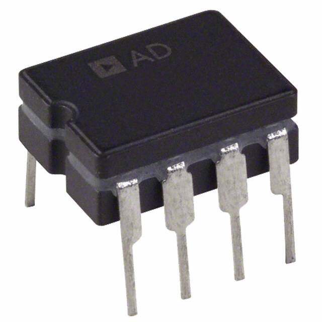
ICGOO电子元器件商城为您提供AD622ANZ由Analog设计生产,在icgoo商城现货销售,并且可以通过原厂、代理商等渠道进行代购。 AD622ANZ价格参考¥38.74-¥59.24。AnalogAD622ANZ封装/规格:线性 - 放大器 - 仪表,运算放大器,缓冲器放大器, 仪表 放大器 1 电路 8-PDIP。您可以下载AD622ANZ参考资料、Datasheet数据手册功能说明书,资料中有AD622ANZ 详细功能的应用电路图电压和使用方法及教程。
| 参数 | 数值 |
| -3db带宽 | 1MHz |
| 3dB带宽 | 1 MHz |
| 产品目录 | 集成电路 (IC)半导体 |
| 描述 | IC OPAMP INSTR 1MHZ 8DIP仪表放大器 LOW COST |
| 产品分类 | Linear - Amplifiers - Instrumentation, OP Amps, Buffer Amps集成电路 - IC |
| 品牌 | Analog Devices |
| 产品手册 | |
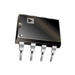
| 产品图片 |
|
| rohs | 符合RoHS无铅 / 符合限制有害物质指令(RoHS)规范要求 |
| 产品系列 | 放大器 IC,仪表放大器,Analog Devices AD622ANZ- |
| 数据手册 | |
| 产品型号 | AD622ANZ |
| 产品培训模块 | http://www.digikey.cn/PTM/IndividualPTM.page?site=cn&lang=zhs&ptm=25193http://www.digikey.cn/PTM/IndividualPTM.page?site=cn&lang=zhs&ptm=30008http://www.digikey.cn/PTM/IndividualPTM.page?site=cn&lang=zhs&ptm=26202 |
| 产品目录页面 | |
| 产品种类 | 仪表放大器 |
| 供应商器件封装 | 8-PDIP |
| 共模抑制比—最小值 | 103 dB |
| 关闭 | No Shutdown |
| 包装 | 管件 |
| 单电源电压 | - |
| 压摆率 | 1.2 V/µs |
| 双重电源电压 | 2.6 V to 18 V |
| 可用增益调整 | 1 V/V to 1000 V/V |
| 商标 | Analog Devices |
| 增益带宽生成 | - |
| 增益带宽积 | - |
| 安装类型 | 通孔 |
| 安装风格 | Through Hole |
| 封装 | Tube |
| 封装/外壳 | 8-DIP(0.300",7.62mm) |
| 封装/箱体 | PDIP-8 |
| 工作温度 | -40°C ~ 85°C |
| 工作温度范围 | - 40 C to + 85 C |
| 工作电源电压 | 2.6 V to 18 V |
| 工厂包装数量 | 50 |
| 带宽 | 1 MHz |
| 放大器类型 | Instrumentation Amplifier |
| 最大功率耗散 | 650 mW |
| 最大工作温度 | + 85 C |
| 最大输入电阻 | 20 kOhms at +/- 15 V |
| 最大输入补偿电流 | 2.5 nA |
| 最小工作温度 | - 40 C |
| 标准包装 | 50 |
| 电压-电源,单/双 (±) | ±2.6 V ~ 18 V |
| 电压-输入失调 | 60µV |
| 电流-电源 | 900µA |
| 电流-输入偏置 | 2nA |
| 电流-输出/通道 | 18mA |
| 电源电流 | 900 uA |
| 电路数 | 1 |
| 系列 | AD622 |
| 视频文件 | http://www.digikey.cn/classic/video.aspx?PlayerID=1364138032001&width=640&height=505&videoID=2245193153001http://www.digikey.cn/classic/video.aspx?PlayerID=1364138032001&width=640&height=505&videoID=2245193159001 |
| 转换速度 | 1.2 V/us |
| 输入偏压电流—最大 | 2 nA |
| 输入补偿电压 | 60 uV |
| 输出电流 | - |
| 输出类型 | - |
| 通道数量 | 1 Channel |




- 商务部:美国ITC正式对集成电路等产品启动337调查
- 曝三星4nm工艺存在良率问题 高通将骁龙8 Gen1或转产台积电
- 太阳诱电将投资9.5亿元在常州建新厂生产MLCC 预计2023年完工
- 英特尔发布欧洲新工厂建设计划 深化IDM 2.0 战略
- 台积电先进制程称霸业界 有大客户加持明年业绩稳了
- 达到5530亿美元!SIA预计今年全球半导体销售额将创下新高
- 英特尔拟将自动驾驶子公司Mobileye上市 估值或超500亿美元
- 三星加码芯片和SET,合并消费电子和移动部门,撤换高东真等 CEO
- 三星电子宣布重大人事变动 还合并消费电子和移动部门
- 海关总署:前11个月进口集成电路产品价值2.52万亿元 增长14.8%



PDF Datasheet 数据手册内容提取
Low Cost Instrumentation Amplifier Data Sheet AD622 FEATURES PIN CONFIGURATION Easy to use RG 1 AD622 8 RG Low cost solution –IN 2 7 +VS Higher performance than two or three op amp design UOnpittiyo ngaali ng awinitsh w nioth e xotneer neaxlt erernsiaslt orers istor –+VINS 34 65 OREUFTPUT 00777-001 (Gain range: 2 to 1000) Figure 1. 8-Lead PDIP and 8-Lead SOIC_N (N and R Suffixes) Wide power supply range: ±2.6 V to ±15 V Available in 8-lead PDIP and 8-lead SOIC_N packages GENERAL DESCRIPTION Low power, 1.5 mA maximum supply current The AD622 is a low cost, moderately accurate instrumentation DC performance amplifier in the traditional pin configuration that requires only 0.15% gain accuracy: G = 1 one external resistor to set any gain between 2 and 1000. For a 125 µV maximum input offset voltage gain of 1, no external resistor is required. The AD622 is a 1.0 µV/°C maximum input offset drift complete difference or subtractor amplifier system that also 5 nA maximum input bias current provides superior linearity and common-mode rejection by 66 dB minimum common-mode rejection ratio: G = 1 incorporating precision laser-trimmed resistors. Noise 12 nV/√Hz @ 1 kHz input voltage noise The AD622 replaces low cost, discrete, two or three op amp 0.60 µV p-p noise: 0.1 Hz to 10 Hz, G = 10 instrumentation amplifier designs and offers good common- AC characteristics mode rejection, superior linearity, temperature stability, 800 kHz bandwidth: G = 10 reliability, power, and board area consumption. The low cost of 10 µs settling time to 0.1% @ G = 1 to 100 the AD622 eliminates the need to design discrete 1.2 V/µs slew rate instrumentation amplifiers to meet stringent cost targets. While providing a lower cost solution, it also provides performance APPLICATIONS and space improvements. Transducer interface Low cost thermocouple amplifier Table 1. Next Generation Upgrades for AD622 Industrial process controls Part Comment Difference amplifier AD8221 Better specs at lower price Low cost data acquisition AD8222 Dual channel or differential out AD8226 Low power, wide input range AD8220 JFET input AD8228 Best gain accuracy AD8295 +2 precision op amps or differential out AD8421 Low noise, better specs Rev. E Information furnished by Analog Devices is believed to be accurate and reliable. However, no responsibility is assumed by Analog Devices for its use, nor for any infringements of patents or other One Technology Way, P.O. Box 9106, Norwood, MA 02062-9106, U.S.A. rliicgehntsse o ifs t hgirradn pteadrt bieys itmhaptl imcaatyio rne sourl to ftrhoemrw itiss ue suen. Sdpeer cainficya ptiaotnesn st uobr jpecatt eton tc hriagnhgtse owf iAthnoaulot gn oDteicvei.c Neso. Tel: 781.329.4700 www.analog.com Trademarks and registered trademarks are the property of their respective owners. Fax: 781.461.3113 ©1996–2012 Analog Devices, Inc. All rights reserved.
AD622 Data Sheet TABLE OF CONTENTS Features .............................................................................................. 1 Theory of Operation .........................................................................9 Applications ....................................................................................... 1 Make vs. Buy: A Typical Application Error Budget ..................9 Pin Configuration ............................................................................. 1 Gain Selection ................................................................................. 11 General Description ......................................................................... 1 Input and Output Offset Voltage .............................................. 11 Revision History ............................................................................... 2 Reference Terminal .................................................................... 11 Specifications ..................................................................................... 3 Input Protection ......................................................................... 11 Absolute Maximum Ratings ............................................................ 5 RF Interference ........................................................................... 12 Thermal Resistance ...................................................................... 5 Ground Returns for Input Bias Currents ................................ 12 ESD Caution .................................................................................. 5 Outline Dimensions ....................................................................... 13 Typical Performance Characteristics ............................................. 6 Ordering Guide .......................................................................... 14 REVISION HISTORY 6/12—Rev. D to Rev. E Added Large Input Voltages at Large Gains Section ................. 11 Changes to General Description Section; Added Table 1 ........... 1 Replaced RF Interference Section ................................................ 11 Changes to Theory of Operation Section and Figure 16 ............. 9 Deleted Grounding Section .......................................................... 10 Changes to Table 5 .......................................................................... 10 Deleted Figure 16 ............................................................................ 10 Changes to Input Selection Section; Deleted Large Input Changes to Ground Returns for Input Bias Currents Section .. 12 Voltages at Large Gains Section; Added Figure 18, Renumbered Updated Outline Dimensions ....................................................... 13 Sequentially ..................................................................................... 11 Changes to Ordering Guide .......................................................... 14 Changes to Ordering Guide .......................................................... 14 4/99—Rev. B to Rev. C 8/07—Rev. C to Rev. D 8/98—Rev. A to Rev. B Updated Format .................................................................. Universal Added Thermal Resistance Section ............................................... 5 2/97—Rev. 0 to Rev. A Added Figure 16 ................................................................................ 9 1/96—Revision 0: Initial Version Rev. E | Page 2 of 16
Data Sheet AD622 SPECIFICATIONS T = 25°C, V = ±15 V, and R = 2 kΩ typical, unless otherwise noted. A S L Table 2. Parameter Conditions Min Typ Max Unit GAIN G = 1 + (50.5 k/R ) G Gain Range 1 1000 Gain Error1 V = ±10 V OUT G = 1 0.05 0.15 % G = 10 0.2 0.50 % G = 100 0.2 0.50 % G = 1000 0.2 0.50 % Nonlinearity V = ±10 V OUT G = 1 to 1000 R = 10 kΩ 10 ppm L G = 1 to 100 R = 2 kΩ 10 ppm L Gain vs. Temperature Gain = 1 10 ppm/°C Gain > 11 −50 ppm/°C VOLTAGE OFFSET Total RTI Error = V + V /G OSI OSO Input Offset, V V = ±5 V to ±15 V 60 125 µV OSI S Average Temperature Coefficient V = ±5 V to ±15 V 1.0 µV/°C S Output Offset, V V = ±5 V to ±15 V 600 1500 µV OSO S Average Temperature Coefficient V = ±5 V to ±15 V 15 µV/°C S Offset Referred to Input vs. Supply (PSR) V = ±5 V to ±15 V S G = 1 80 100 dB G = 10 95 120 dB G = 100 110 140 dB G = 1000 110 140 dB INPUT CURRENT Input Bias Current 2.0 5.0 nA Average Temperature Coefficient 3.0 pA/°C Input Offset Current 0.7 2.5 nA Average Temperature Coefficient 2.0 pA/°C INPUT Input Impedance Differential 10||2 G Ω||pF Common Mode 10||2 GΩ||pF Input Voltage Range2 V = ±2.6 V to ±5 V −V + 1.9 +V – 1.2 V S S S Over Temperature −V + 2.1 +V – 1.3 V S S V = ±5 V to ±18 V −V + 1.9 +V – 1.4 V S S S Over Temperature −V + 2.1 +V – 1.4 V S S Common-Mode Rejection Ratio V = 0 V to ±10 V CM DC to 60 Hz with 1 kΩ Source Imbalance G = 1 66 78 dB G = 10 86 98 dB G = 100 103 118 dB G = 1000 103 118 dB OUTPUT Output Swing R = 10 kΩ L V = ±2.6 V to ±5 V −V + 1.1 +V – 1.2 V S S S Over Temperature −V + 1.4 +V – 1.3 V S S V = ±5 V to ±18 V −V + 1.2 +V – 1.4 V S S S Over Temperature −V + 1.6 +V – 1.5 V S S Short Current Circuit ±18 mA Rev. E | Page 3 of 16
AD622 Data Sheet Parameter Conditions Min Typ Max Unit DYNAMIC RESPONSE Small Signal −3 dB Bandwidth G = 1 1000 kHz G = 10 800 kHz G = 100 120 kHz G = 1000 12 kHz Slew Rate 1.2 V/µs Settling Time to 0.1% 10 V step G = 1 to 100 10 µs NOISE Voltage Noise, 1 kHz Total RTI Noise = √(e2 ) + (e ∕G)2 ni no Input Voltage Noise, e 12 nV/√Hz ni Output Voltage Noise, e 72 nV/√Hz no RTI, 0.1 Hz to 10 Hz G = 1 4.0 µV p-p G = 10 0.6 µV p-p G = 100 0.3 µV p-p Current Noise f = 1 kHz 100 fA/√Hz 0.1 Hz to 10 Hz 10 pA p-p REFERENCE INPUT R 20 kΩ IN I V , V = 0 50 60 µA IN IN+ REF Voltage Range −V + 1.6 +V – 1.6 V S S Gain to Output 1 ± 0.0015 POWER SUPPLY Operating Range3 ±2.6 ±18 V Quiescent Current V = ±2.6 V to ±18 V 0.9 1.3 mA S Over Temperature 1.1 1.5 mA TEMPERATURE RANGE For Specified Performance −40 to +85 °C 1 Does not include effects of External Resistor RG. 2 One input grounded, G = 1. 3 Defined as the same supply range that is used to specify PSR. Rev. E | Page 4 of 16
Data Sheet AD622 ABSOLUTE MAXIMUM RATINGS THERMAL RESISTANCE Table 3. θ is specified for the device in free air. Parameter Rating JA Supply Voltage ±18 V Table 4. Thermal Resistance Internal Power Dissipation1 650 mW Package Type θ Unit JA Input Voltage (Common Mode) ±V S 8-Lead PDIP (N-8) 95 °C/W Differential Input Voltage2 ±25 V 8-Lead SOIC_N (R-8) 155 °C/W Output Short Circuit Duration Indefinite Storage Temperature Range −65°C to +125°C Operating Temperature Range −40°C to +85°C ESD CAUTION Lead Temperature (Soldering, 10 sec) 300°C 1 Specification is for device in free air; see Table 4. 2 May be further restricted for gains greater than 14. See the Input Protection section for more information. Stresses above those listed under Absolute Maximum Ratings may cause permanent damage to the device. This is a stress rating only; functional operation of the device at these or any other conditions above those indicated in the operational section of this specification is not implied. Exposure to absolute maximum rating conditions for extended periods may affect device reliability. Rev. E | Page 5 of 16
AD622 Data Sheet TYPICAL PERFORMANCE CHARACTERISTICS T = 25°C, V = ±15 V, R = 2 kΩ, unless otherwise noted. A S L 50 1000 SAMPLE SIZE = 191 40 OF UNITS 30 E (nV/ Hz) 100 GAIN = 1 AGE NOIS GAIN = 10 PERCENT 20 VOLTAGE 10 GAIN = 100, 1000 10 GAIN = 1000 BW LIMIT 0–1.2 –0.8 OUT–P0U.4T OFFSE0T VOLTAG0.E4 (mV) 0.8 1.2 00777-002 11 10 F1R0E0QUENCY (1Hkz) 10k 100k 00777-005 Figure 2. Typical Distribution of Output Offset Voltage Figure 5. Voltage Noise Spectral Density vs. Frequency (G = 1 to 1000) 50 1000 SAMPLE SIZE = 383 40 TS Hz) UNI A/ OF 30 E (f GE OIS 100 A N ENT 20 ENT C R R R E U P C 10 0 60 COMMO80N-MODE R1E0J0ECTION R1A2T0IO (dB) 140 00777-003 101 10FREQUENCY (Hz)100 1000 00777-006 Figure 3. Typical Distribution of Common-Mode Rejection Figure 6. Current Noise Spectral Density vs. Frequency 2.0 140 120 G = 1000 V) E (µ 1.5 100 G = 100 G A G = 10 T OL B) 80 T V 1.0 R (d G = 1 E M FS C 60 F O T U 40 P 0.5 N I 20 00 1 WARM2-UP TIME (M3inutes) 4 5 00777-004 00.1 1 10 FR1E0Q0UENCY1 k(Hz) 10k 100k 1M 00777-007 Figure 4. Change in Input Offset Voltage vs. Warm-Up Time Figure 7. CMR vs. Frequency, RTI, 0 kΩ to 1 kΩ Source Imbalance Rev. E | Page 6 of 16
Data Sheet AD622 180 30 VS = ±15V G = 10 160 p) p- 140 V PSR (dB) 120 G = 1000 E SWING ( 20 POSITIVE 10800 G = 100 T VOLTAG 10 U 60 G = 10 UTP O 40 G = 1 200.1 1 10 FR1E0Q0UENCY1 k(Hz) 10k 100k 1M 00777-008 010 1L0O0AD RESISTANCE (1Ωk) 10k 00777-011 Figure 8. Positive PSR vs. Frequency, RTI (G = 1 to 1000) Figure 11. Output Voltage Swing vs. Load Resistance 180 20 160 140 15 B) s) SR (d 120 ME (µ TO 0.1% P TI E 100 G 10 GATIV 80 G = 1000 TTLIN E E N S 60 G = 100 5 40 G = 10 G = 1 200.1 1 10 FR1E0Q0UENCY1 k(Hz) 10k 100k 1M 00777-009 00 5 OUTPUT S1T0EP SIZE (V) 15 20 00777-012 Figure 9. Negative PSR vs. Frequency, RTI (G = 1 to 1000) Figure 12. Settling Time vs. Step Size (G = 1) 1000 1000 100 µs) 100 V) ME ( N (V/ 10 G TI GAI LIN T T E 10 S 1 0.1 1 100 1k F1R0EkQUENCY1 (0H0zk) 1M 10M 00777-010 1 10 GAIN 100 1000 00777-013 Figure 10. Gain vs. Frequency Figure 13. Settling Time to 0.1% vs. Gain, for a 10 V Step Rev. E | Page 7 of 16
AD622 Data Sheet 10kΩ 1kΩ 10kΩ INPUT 0.01% POT 0.1% 20V p-p VOUT 100 100kΩ 0.1% 90 +VS 11kΩ 1kΩ 100Ω 2 7 Ø 0.1% 0.1% 0.1% 1 G = 1000 G = 1 AD622 6 G = 100 G = 10 8 5 01%0 51.1Ω 511Ω 5.62kΩ 3 4 10µV 2V 00777-014 –VS 00777-015 Figure 14. Gain Nonlinearity, G = 1, RL = 10 kΩ (20 µV = 2 ppm) Figure 15. Settling Time Test Circuit Rev. E | Page 8 of 16
Data Sheet AD622 THEORY OF OPERATION The value of R also determines the transconductance of the The AD622 is a monolithic instrumentation amplifier based on G preamp stage. As R is reduced for larger gains, the trans- a modification of the classic three op amp approach. Absolute G conductance increases asymptotically to that of the input value trimming allows the user to program gain accurately (to transistors. This has the following three important advantages: 0.5% at G = 1000) with only one resistor. Monolithic construction and laser wafer trimming allow the tight matching and tracking • Open-loop gain is boosted for increasing programmed of circuit components, thus insuring AD622 performance. gain, thus reducing gain-related errors. Input Transistor Q1 and Input Transistor Q2 provide a single • The gain-bandwidth product (determined by C1, C2, and differential-pair bipolar input for high precision (see Figure 16). the preamp transconductance) increases with programmed Feedback through the Q1-A1-R1 loop and the Q2-A2-R2 loop gain, thus optimizing frequency response. maintains constant collector current of the Q1 and Q2 input • The input voltage noise is reduced to a value of 12 nV/√Hz, devices, thereby impressing the input voltage across External determined mainly by the collector current and base Gain-Setting Resistor R . This creates a differential gain from the resistance of the input devices. G inputs to the A1 and A2 outputs given by G = (R1 + R2)/R + 1. G The internal gain resistors, R1 and R2, are trimmed to an Unity-Gain Subtractor A3 removes any common-mode signal, absolute value of 25.25 kΩ, allowing the gain to be programmed yielding a single-ended output referred to the REF pin potential. accurately with a single external resistor. MAKE vs. BUY: A TYPICAL APPLICATION ERROR +VS BUDGET The AD622 offers cost and performance advantages over I1 20µA VB 20µA I2 discrete two op amp instrumentation amplifier designs along with smaller size and fewer components. In a typical application A1 A2 10kΩ shown in Figure 17, a gain of 10 is required to receive and C1 C2 amplify a 0 to 20 mA signal from the AD694 current transmitter. 10kΩ OUTPUT The current is converted to a voltage in a 50 Ω shunt. In A3 applications where transmission is over long distances, line 10kΩ 10kΩ impedance can be significant so that differential voltage REF +VS +VS measurement is essential. Where there is no connection R1 R2 between the ground returns of transmitter and receiver, there Q1 Q2 +IN – IN R3 R4 must be a dc path from each input to ground, implemented in 400Ω RG 400Ω this case using two 1 kΩ resistors. The error budget detailed in GAIN GAIN SENSE SENSE Table 5 shows how to calculate the effect of various error –VS 00777-022 s ources on circuit accuracy. Figure 16. Simplified Schematic of the AD622 + RL2 1kΩ 10Ω VIN LT11/0213 1/2 0 ATOD 6209m4A 0 TO 20mA 50Ω 1kΩ RG AD622 – LT1013 TRANSMITTER 5.62kΩ 1kΩ RL2 REF 10Ω 1kΩ 9kΩ* 1kΩ* 1kΩ* 9kΩ* *0.1% RESISTOR MATCH, 50ppm/°C TRACKING W0I TTHO 5 200Ωm SAH CUUNRTR IEMNPTE DLOANOCPE AD622 MOANMOPLLITIFHIEICR I,N GS =T R9U.9M86ENTATION HOMEBREW IN-AMP, G = 10 00777-016 Figure 17. Make vs. Buy Rev. E | Page 9 of 16
AD622 Data Sheet The AD622 provides greater accuracy at lower cost. The higher over temperature due to the drift mismatch of the discrete cost of the homebrew circuit is dominated in this case by the resistors. matched resistor network. One could also realize a homebrew Note that for the homebrew circuit, the LT1013 specification for design using cheaper discrete resistors that are either trimmed noise has been multiplied by √2. This is because a two op amp or hand selected to give high common-mode rejection. This type instrumentation amplifier has two op amps at its inputs, level of common-mode rejection, however, degrades significantly both contributing to the overall noise. Table 5. Make vs. Buy Error Budget Total Error in ppm Relative to 1 V FS Error Source AD622 Circuit Calculation Homebrew Circuit Calculation AD622 Homebrew ABSOLUTE ACCURACY at TA = 25°C Total RTI Offset Voltage, µV 125 µV + 1500 µV/10 800 µV × 2 275 1600 Input Offset Current, nA 2.5 nA × 1 kΩ 15 nA × 1 kΩ 2.5 15 CMR, dB 86 dB→50 ppm × 0.5 V (0.1% Match × 0.5 V)/10 V 25 50 Total Absolute Error 302.5 1665 DRIFT TO 85°C Gain Drift, ppm/°C (50 ppm + 5 ppm) × 60°C (50 ppm)/°C × 60°C 3300 3000 Total RTI Offset Voltage, µV/°C (1 µV/°C + 15 µV/°C /10) × 60°C 9 µV/°C × 2 × 60°C 150 1080 Input Offset Current, pA/°C 2 pA/°C × 1 kΩ × 60°C 155 pA/°C × 1 kΩ × 60°C 0.12 9.3 Total Drift Error 3450.12 4089.3 RESOLUTION Gain Nonlinearity, ppm of Full Scale 10 ppm 20 ppm 10 20 Typ 0.1 Hz to 10 Hz Voltage Noise, µV p-p 0.6 µV p-p 0.55 µV p-p × √2 0.6 0.778 Total Resolution Error 10.6 20.778 Grand Total Error 3763 5775 Rev. E | Page 10 of 16
Data Sheet AD622 GAIN SELECTION REFERENCE TERMINAL The AD622 gain is resistor programmed by R or, more G precisely, by whatever impedance appears between Pin 1 and The reference terminal potential defines the zero output voltage Pin 8. The AD622 is designed to offer gains as close as possible and is especially useful when the load does not share a precise to popular integer values using standard 1% resistors. Table 6 ground with the rest of the system. The reference terminal provides shows required values of RG for various gains. Note that for a direct means of injecting a precise offset to the output, with an G = 1, the RG pins are unconnected (RG = ∞). For any arbitrary allowable range of 2 V within the supply voltages. Parasitic gain, RG can be calculated by using the formula resistance should be kept to a minimum for optimum CMR. 50.5kΩ INPUT PROTECTION R = G G−1 The AD622 safely withstands an input current of ±60 mA for To minimize gain error, avoid high parasitic resistance in series several hours at room temperature. This is true for all gains and with R . To minimize gain drift, R should have a low temperature power on and off, which is useful if the signal source and amplifier G G coefficient less than 10 ppm/°C for the best performance. are powered separately. For longer time periods, the input current should not exceed 6 mA. Table 6. Required Values of Gain Resistors For input voltages beyond the supplies, a protection resistor should Desired Calculated be placed in series with each input to limit the current to 6 mA. Gain 1% Std Table Value of R , Ω Gain G These can be the same resistors as those used in the RFI filter. 2 51.1 k 1.988 High values of resistance can impact the noise and AC CMRR 5 12.7 k 4.976 performance of the system. Low leakage diodes (such as the 10 5.62 k 9.986 BAV199) can be placed at the inputs to reduce the required 20 2.67 k 19.91 protection resistance. 33 1.58 k 32.96 40 1.3 k 39.85 +SUPPLY 50 1.02 k 50.50 65 787 65.17 100 511 99.83 200 255 199.0 R +IN 500 102 496.1 VOUT 1000 51.1 989.3 AD622 R INPUT AND OUTPUT OFFSET VOLTAGE REF –IN The low errors of the AD622 are attributable to two sources: input and output errors. The output error is divided by G when rheifgehr rgeadi ntos athned itnhpeu otu. Itnpu ptr earcrtoicres, dthome iinnpautet aetr rloorws gdaoimnsi.n Tathee a t –SUPPLY 00777-023 total VOS for a given gain is calculated as follows: Figure 18. Diode Protection for Voltages Beyond Supply Total Error RTI = input error + (output error/G) Total Error RTO = (input error × G) + output error Rev. E | Page 11 of 16
AD622 Data Sheet RF INTERFERENCE GROUND RETURNS FOR INPUT BIAS CURRENTS RF rectification is often a problem when amplifiers are used in Input bias currents are those currents necessary to bias the applications where there are strong RF signals. The disturbance input transistors of an amplifier. There must be a direct return may appear as a small dc offset voltage. High frequency signals path for these currents; therefore, when amplifying floating can be filtered with a low-pass, RC network placed at the input input sources such as transformers or ac-coupled sources, there of the instrumentation amplifier, as shown in Figure 19. In must be a dc path from each input to ground as shown in addition, this RC input network also provides additional input Figure 20, Figure 21, and Figure 22. Refer to the Designer’s overload protection (see the Input Protection section). Guide to Instrumentation Amplifiers (free from Analog Devices, Inc.) for more information regarding in-amp applications. +VS + +VS 0.1µF 10µF –IN R CC 2 7 4.02kΩ 1nF +IN 1 4.0R2kΩ C47DnF RG AD622 VOUT RG 8 AD6225 6 VOUT CC –IN REF +IN 3 4 REF LOAD 1nF 0.1µF –VS 10µF + 00777-017 Figure 20. Ground Returns for– VBSias Currents with TransformTSGOUReP OrPP UCOLNoWYDuEpRled00777-018 I nputs Figure 19. RFI Suppression Circuit for AD622 Series In-Amps +VS –IN 2 7 The filter limits the input signal bandwidth to the following 1 cutoff frequencies: RG AD622 6 VOUT 1 8 5 FilterFreq = 3 4 LOAD DIFF 2πR(2C +C ) +IN REF D C FilterFreqCM =2πR1C –VS TSGOURP OPPUOLNWYDER 00777-019 C Figure 21. Ground Returns for Bias Currents with Thermocouple Inputs where C ≥ 10C . D C +VS Figure 19 shows an example where the differential filter –IN 2 7 frequency is approximately 400 Hz, and the common-mode 1 filter frequency is approximately 40 kHz. With this differential RG AD622 6 VOUT filter in place and operating at gain of 1000, the typical dc offset 8 5 shift over a frequency range of 1 Hz to 20 MHz is less than 1.5 µV 3 4 LOAD +IN REF RTI, and the RF signal rejection of the circuit is better than 100kΩ 100kΩ 7R1T dI,B a.n Adt RaF g areinje octfi 1o0n0 i,s t ghree datce or ftfhsaent s7h0if dt Bis. well below 1 mV –VS TSGOURP OPPUOLNWYDER 00777-020 Figure 22. Ground Returns for Bias Currents with AC-Coupled Inputs The input resistors should be selected to be high enough to isolate the sensor from the C and C capacitors but low C D enough not to influence system noise. Mismatch between R × C at the positive input and R × C at the negative input C C degrades the CMRR of the AD622. Therefore, the C capacitors C should be high precision types such as NPO/COG ceramics. The tolerance of the C capacitor is less critical. D Rev. E | Page 12 of 16
Data Sheet AD622 OUTLINE DIMENSIONS 0.400 (10.16) 0.365 (9.27) 0.355 (9.02) 8 5 0.280 (7.11) 0.250 (6.35) 1 4 0.240 (6.10) 0.325 (8.26) 0.310 (7.87) 0.100 (2.54) 0.300 (7.62) BSC 0.060 (1.52) 0.195 (4.95) 0.210 (5.33) MAX 0.130 (3.30) MAX 0.115 (2.92) 0.015 0.150 (3.81) (0.38) 0.015 (0.38) 0.130 (3.30) MIN GAUGE 0.115 (2.92) SEATING PLANE 0.014 (0.36) PLANE 0.010 (0.25) 0.022 (0.56) 0.008 (0.20) 0.005 (0.13) 0.430 (10.92) 0.018 (0.46) MIN MAX 0.014 (0.36) 0.070 (1.78) 0.060 (1.52) 0.045 (1.14) COMPLIANTTO JEDEC STANDARDS MS-001 CONTROLLING DIMENSIONSARE IN INCHES; MILLIMETER DIMENSIONS (RCINEOFRPEANRREERENN LCTEEHA EODSNSEL MSY)AAAYNR BDEE AR CROOEU NNNFODIGETUDAR-POEPFDRFOA INSPC RWHIAH ETOEQL UFEIO VORAR LU EHSNAETL ISFN FLDOEEARSDIGSN.. 070606-A Figure 23. 8-Lead Plastic Dual In-Line Package [PDIP] Narrow Body (N-8) Dimensions shown in inches and (millimeters) 5.00(0.1968) 4.80(0.1890) 8 5 4.00 (0.1574) 6.20 (0.2441) 3.80 (0.1497) 1 4 5.80 (0.2284) 1.27 (0.0500) 0.50 (0.0196) BSC 1.75 (0.0688) 0.25 (0.0099) 45° 0.25 (0.0098) 1.35 (0.0532) 8° 0.10 (0.0040) 0° COPLANARITY 0.51 (0.0201) 0.10 SEATING 0.31 (0.0122) 0.25 (0.0098) 10..2470 ((00..00510507)) PLANE 0.17 (0.0067) COMPLIANTTO JEDEC STANDARDS MS-012-AA C(RINOEFNPEATRRREOENNLCLTEIHN EOGSN EDLSIYM)AEANNRDSEI AORRNOESU NANORDEET DAIN-PO MPFRIFLO LMPIIMRLELIATIMTEEER TFSEO; RIRN ECUQHSU EDI VIINMA LEDENENSSTIIOGSN NFS.OR 012407-A Figure 24. 8-Lead Standard Small Outline Package [SOIC_N] Narrow Body (R-8) Dimensions shown in millimeters and (inches) Rev. E | Page 13 of 16
AD622 Data Sheet ORDERING GUIDE Model1 Temperature Range Package Description Package Option AD622ANZ −40°C to +85°C 8-Lead PDIP N-8 AD622AR –40°C to +85°C 8-Lead SOIC_N R-8 AD622AR-REEL –40°C to +85°C 8-Lead SOIC_N R-8 AD622AR-REEL7 –40°C to +85°C 8-Lead SOIC_N R-8 AD622ARZ –40°C to +85°C 8-Lead SOIC_N R-8 AD622ARZ-RL –40°C to +85°C 8-Lead SOIC_N R-8 AD622ARZ-R7 –40°C to +85°C 8-Lead SOIC_N R-8 1 Z = RoHS Compliant Part. Rev. E | Page 14 of 16
Data Sheet AD622 NOTES Rev. E | Page 15 of 16
AD622 Data Sheet NOTES ©1996–2012 Analog Devices, Inc. All rights reserved. Trademarks and registered trademarks are the property of their respective owners. D00777-0-6/12(E) Rev. E | Page 16 of 16
Mouser Electronics Authorized Distributor Click to View Pricing, Inventory, Delivery & Lifecycle Information: A nalog Devices Inc.: AD622ANZ AD622ARZ AD622AR AD622AR-REEL7 AD622ARZ-R7 AD622ARZ-RL
 Datasheet下载

