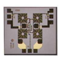
ICGOO在线商城 > 射频/IF 和 RFID > RF 混频器 > AD608ARZ
- 型号: AD608ARZ
- 制造商: Analog
- 库位|库存: xxxx|xxxx
- 要求:
| 数量阶梯 | 香港交货 | 国内含税 |
| +xxxx | $xxxx | ¥xxxx |
查看当月历史价格
查看今年历史价格
AD608ARZ产品简介:
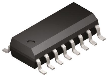
ICGOO电子元器件商城为您提供AD608ARZ由Analog设计生产,在icgoo商城现货销售,并且可以通过原厂、代理商等渠道进行代购。 AD608ARZ价格参考¥23.29-¥25.00。AnalogAD608ARZ封装/规格:RF 混频器, RF Mixer IC FM, GSM, PM, PHS, FM Down Converter 500MHz 16-SOIC。您可以下载AD608ARZ参考资料、Datasheet数据手册功能说明书,资料中有AD608ARZ 详细功能的应用电路图电压和使用方法及教程。
AD608ARZ是Analog Devices Inc.(ADI公司)生产的一款RF混频器,广泛应用于无线通信、雷达系统、测试与测量设备等领域。其主要应用场景包括但不限于以下几个方面:

1. 无线通信系统:AD608ARZ可以用于各种无线通信系统的中频(IF)到射频(RF)转换或反之。它能够处理从低频到高频的信号,适用于GSM、CDMA、Wi-Fi等通信标准。该器件具有高线性度和低噪声系数,确保了通信系统的高质量信号传输。

2. 雷达系统:在雷达应用中,AD608ARZ可用于发射和接收链路中的频率转换。它能够将接收到的高频雷达回波信号下变频为较低频率的中频信号,便于后续处理。同时,在发射端,它可以将基带信号上变频至所需的发射频率,实现高效的信号调制和发射。

3. 测试与测量设备:AD608ARZ也常用于频谱分析仪、信号发生器等测试设备中。这些设备需要精确地进行频率转换,以准确测量和生成不同频率的信号。AD608ARZ的高性能特性使其成为这些应用的理想选择。

4. 卫星通信:在卫星通信领域,AD608ARZ可以用于地面站设备中的频率转换。它能够有效地处理卫星通信所需的高频段信号,提供稳定的性能表现,确保数据传输的可靠性和准确性。

总之,AD608ARZ凭借其优异的技术指标和可靠性,成为多种高频应用场合下的关键组件。无论是民用还是军用市场,它都能满足用户对高性能RF混频器的需求。
| 参数 | 数值 |
| 产品目录 | |
| 描述 | IC MIXER 500MHZ DOWN CONV 16SOIC时钟发生器及支持产品 Mixer/Limiter/RSSI 3V Rcvr IF Subsystem |
| DevelopmentKit | EVAL-AD608EBZ |
| 产品分类 | |
| 品牌 | Analog Devices |
| 产品手册 | |
| 产品图片 |
|
| rohs | 符合RoHS无铅 / 符合限制有害物质指令(RoHS)规范要求 |
| 产品系列 | 时钟和计时器IC,时钟发生器及支持产品,Analog Devices AD608ARZAD608 |
| 数据手册 | |
| 产品型号 | AD608ARZ |
| RF类型 | FM,GSM,PM,PHS,FM |
| 产品目录页面 | |
| 产品种类 | 时钟发生器及支持产品 |
| 供应商器件封装 | 16-SOIC |
| 包装 | 管件 |
| 商标 | Analog Devices |
| 噪声系数 | 16dB |
| 增益 | 24dB |
| 封装 | Tube |
| 封装/外壳 | 16-SOIC(0.154",3.90mm 宽) |
| 封装/箱体 | SOIC N |
| 工作电源电压 | 3 V |
| 工厂包装数量 | 48 |
| 最大工作温度 | + 85 C |
| 最大输入频率 | 500 MHz (Typ) |
| 最大输出频率 | 30 MHz |
| 最小工作温度 | - 25 C |
| 标准包装 | 48 |
| 混频器数 | 1 |
| 电压-电源 | 2.7 V ~ 5.5 V |
| 电流-电源 | 7.3mA |
| 系列 | AD608 |
| 视频文件 | http://www.digikey.cn/classic/video.aspx?PlayerID=1364138032001&width=640&height=505&videoID=2245193150001 |
| 辅助属性 | 降频变频器 |
| 频率 | 500MHz |


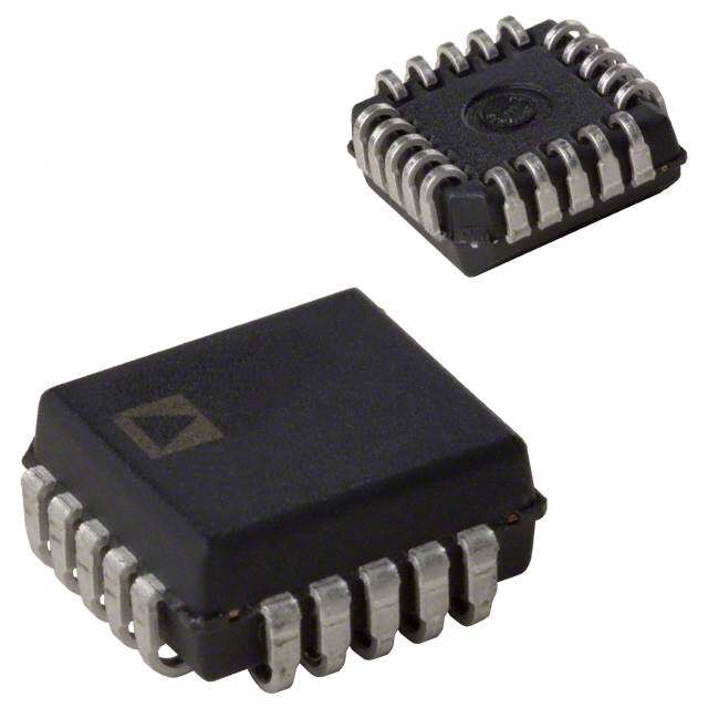
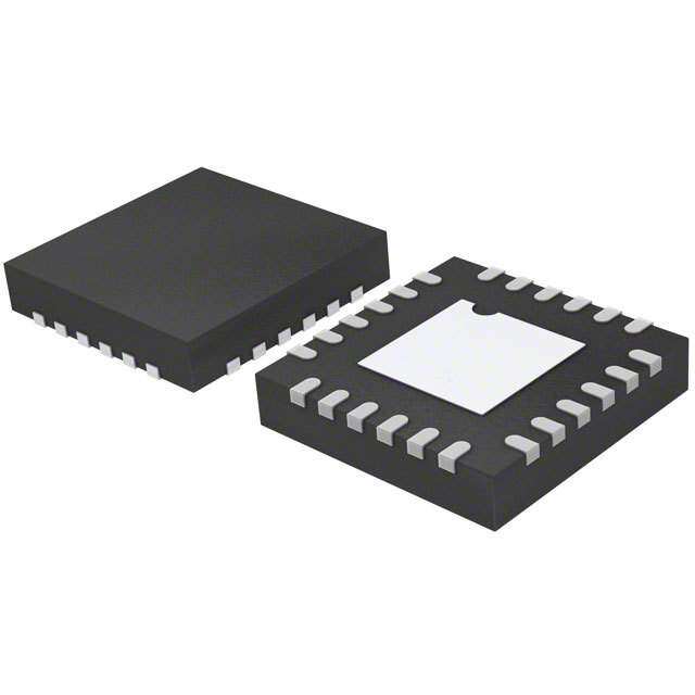

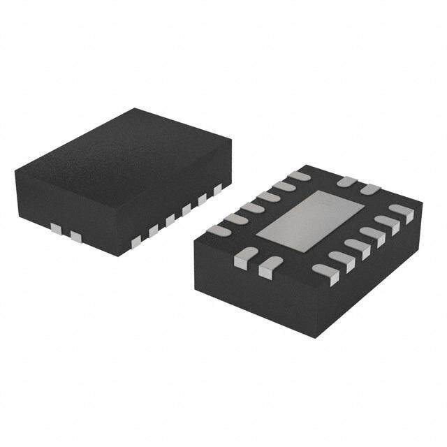


- 商务部:美国ITC正式对集成电路等产品启动337调查
- 曝三星4nm工艺存在良率问题 高通将骁龙8 Gen1或转产台积电
- 太阳诱电将投资9.5亿元在常州建新厂生产MLCC 预计2023年完工
- 英特尔发布欧洲新工厂建设计划 深化IDM 2.0 战略
- 台积电先进制程称霸业界 有大客户加持明年业绩稳了
- 达到5530亿美元!SIA预计今年全球半导体销售额将创下新高
- 英特尔拟将自动驾驶子公司Mobileye上市 估值或超500亿美元
- 三星加码芯片和SET,合并消费电子和移动部门,撤换高东真等 CEO
- 三星电子宣布重大人事变动 还合并消费电子和移动部门
- 海关总署:前11个月进口集成电路产品价值2.52万亿元 增长14.8%


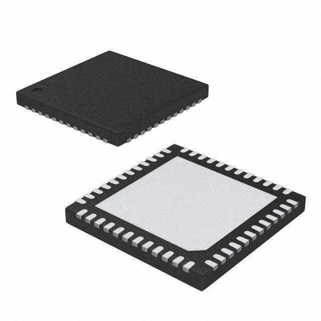
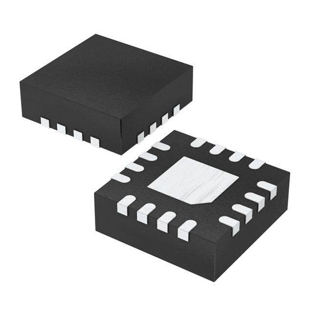
PDF Datasheet 数据手册内容提取
Low Power Mixer/Limiter/RSSI 3 V Receiver IF Subsystem AD608 FEATURES The RF and local oscillator (LO) bandwidths both exceed 500 MHz. In a typical IF application, the AD608 can accept the Mixer output of a 240 MHz surface acoustic wave (SAW) filter and down- −15 dBm, 1 dB compression point convert it to a nominal 10.7 MHz IF with a conversion gain of −5 dBm IP3 24 dB (Z = 165 Ω). The AD608 logarithmic/limiting amplifier 24 dB conversion gain IF section handles any IF from low frequency (LF) up to 30 MHz. >500 MHz input bandwidth Logarithmic/limiting amplifier The mixer is a doubly balanced gilbert-cell mixer and operates 80 dB RSSI range linearly for RF inputs spanning −95 dBm to −15 dBm. It has a ±3° phase stability over 80 dB range nominal −5 dBm third-order intercept. An on-board LO pre- Low power amplifier requires only −16 dBm of LO drive. The current output 21 mW at 3 V power consumption of the mixer drives a reverse-terminated, industry-standard CMOS-compatible power-down to 300 μW typical 10.7 MHz, 330 Ω filter. 200 ns enable/disable time The nominal logarithmic scaling is such that the output is +0.2 V APPLICATIONS for a sinusoidal input to the IF amplifier of −75 dBm and +1.8 V at an input of +5 dBm; over this range, the logarithmic confor- PHS, GSM, TDMA, FM, or PM receivers mance is typically ±1 dB. The logarithmic slope is proportional Battery-powered instrumentation to the supply voltage. A feedback loop automatically nulls the Base station RSSI measurements input offset of the first stage down to the submicrovolt level. The AD608 limiter output provides a hard-limited signal output GENERAL DESCRIPTION at 400 mV p-p. The voltage gain of the limiting amplifier to this The AD608 provides a low power, low distortion, low noise mixer output is more than 100 dB. Transition times are 11 ns and the as well as a complete, monolithic logarithmic/limiting amplifier phase is stable to within ±3° at 10.7 MHz for signals from −75 dBm that uses a successive-detection technique. In addition, the AD608 to +5 dBm. provides both a high speed received signal strength indicator The AD608 is enabled by a CMOS logic-level voltage input, (RSSI) output with 80 dB dynamic range and a hard-limited with a response time of 200 ns. When disabled, the standby output. The RSSI output is from a two-pole postdemodulation power is reduced to 300 μW within 400 ns. low-pass filter and provides a loadable output voltage of 0.2 V to 1.8 V. The AD608 operates from a single 2.7 V to 5.5 V supply The AD608 is specified for the industrial temperature range of at a typical power level of 21 mW at 3 V. −25°C to +85°C for 2.7 V to 5.5 V supplies and −40°C to +85°C for 3.0 V to 5.5 V supplies. This device comes in a 16-lead plastic SOIC. FUNCTIONAL BLOCK DIAGRAM 24dB MIXER GAIN IN3SdEBR NTIOOMNI NLAOLSS 110dB9 0LdIMB IRTESRSI GAIN RFHI 5 ±(±68m90Am MVA IXN TOOU T16P5UΩT) –7+IF51 d5INdBBPmUm TT2O RE7C FTUIFLILE-RW CAEVLELS 2LMPHFz CROSMS3I 1121 R200.S2mSVVI T/OdOUB 1T.P8VUT –9R5–dF1B 5IdRNmBFP TmLUOOT1 6 PREAMLOPMIXER MIDSUDPRBVPMIPVMLXFEYIODRP87 330ΩB1A01F0N0In.DL7FT-MPEHAR+z3S3S0Ω101+00ΩnF 190IIFFHLIO 5-S(1T6AdGBE P IEFR A SMTPALGIFEI)ER LFIMINITAELRLVMPOSP2 1154 +LO420IUM.07TmIVTPV EUT RpOT- p5.5V IF BIAS + 13 BIAS 18nF FDBK AD608 ±50µA VPS1 COM1 LOHICOM2 PRUP 1 2 3 4 16 2.7V TO LO INPUT CMOS LOGIC 5.5V –16dBm INPUT 12–3195.7d6BµmV R=M±5S6 TmOV 3M9A7.X6ImMVU MRM FSO FRO LRIN±E1AdRB ORPSESRI AACTCIOUNR.ACY. Figure 1. 07886-001 Rev. C Information furnished by Analog Devices is believed to be accurate and reliable. However, no responsibility is assumed by Analog Devices for its use, nor for any infringements of patents or other One Technology Way, P.O. Box 9106, Norwood, MA 02062-9106, U.S.A. rights of third parties that may result from its use. Specifications subject to change without notice. No license is granted by implication or otherwise under any patent or patent rights of Analog Devices. Tel: 781.329.4700 www.analog.com Trademarks and registered trademarks are the property of their respective owners. Fax: 781.461.3113 ©1996–2009 Analog Devices, Inc. All rights reserved.
AD608 TABLE OF CONTENTS Features .............................................................................................. 1 Mixer ...............................................................................................9 Applications ....................................................................................... 1 Mixer Gain .....................................................................................9 General Description ......................................................................... 1 IF Filter Terminations ................................................................ 10 Functional Block Diagram .............................................................. 1 The Logarithmic IF Amplifier .................................................. 10 Revision History ............................................................................... 2 Offset Feedback Loop ................................................................ 10 Specifications ..................................................................................... 3 RSSI Output ................................................................................ 11 Absolute Maximum Ratings ............................................................ 4 Digitizing the RSSI ..................................................................... 11 Thermal Resistance ...................................................................... 4 Power Consumption .................................................................. 11 ESD Caution .................................................................................. 4 Troubleshooting .......................................................................... 11 Pin Configuration and Function Descriptions ............................. 5 Applications Information .............................................................. 12 Typical Performance Characteristics ............................................. 6 Outline Dimensions ....................................................................... 13 Test Circuits ....................................................................................... 8 Ordering Guide .......................................................................... 13 Theory of Operation ........................................................................ 9 REVISION HISTORY 2/09—Rev. B to Rev. C Updated Format .................................................................. Universal Reorganized Layout ............................................................ Universal Change to General Description Section ........................................ 1 Changes to DC Level Parameter, Operating Range Parameter, and T to T Parameter, Table 1 .......................................... 3 MIN MAX Added Typical Performance Characteristics Heading ................ 6 Added Test Circuits Heading .......................................................... 8 Changes to Figure 17 and Figure 19 ............................................... 8 Change to Figure 22 ......................................................................... 9 Changes to Table 5 ............................................................................ 9 Updated Outline Dimensions ....................................................... 13 Changes to Ordering Guide .......................................................... 13 Rev. C | Page 2 of 16
AD608 SPECIFICATIONS T = 25°C, supply = 3 V, dBm is referred to 50 Ω, unless otherwise noted. A Table 1. Parameter Conditions1 Min Typ Max Unit MIXER PERFORMANCE RF and LO Frequency Range 500 MHz LO Power Input terminated in 50 Ω −16 dBm Conversion Gain Driving doubly terminated 330 Ω IF filter, Z = 165 Ω 19 24 28 dB IF Noise Figure Matched input, f = 100 MHz 11 dB RF Matched input, f = 240 MHz 16 dB RF 1 dB Compression Point Input terminated in 50 Ω −15 dBm Third-Order Intercept f = 240 MHz and 240.02 MHz, f = 229.3 MHz −5 dBm RF LO Input Resistance f = 100 MHz (see Table 5) 1.9 kΩ RF Input Capacitance f = 100 MHz (see Table 5) 3 pF RF LIMITER PERFORMANCE Gain Full temperature and supply range 110 dB Limiting Threshold 3° rms phase jitter at 10.7 MHz −75 dBm 280 kHz IF bandwidth Input Resistance 10 kΩ Input Capacitance 3 pF Phase Variation −75 dBm to +5 dBm IF input signal at 10.7 MHz ±3 Degrees DC Level Center of output swing (VPOS – 1 V) 2 V Output Level Limiter output driving 5 kΩ load 400 mV p-p Rise and Fall Times Driving a 5 pF load 11 ns Output Impedance 200 Ω RSSI PERFORMANCE At 10.7 MHz Nominal Slope At VPOS = 3 V; proportional to VPOS 17.27 20 23.27 mV/dB Nominal Intercept −85 dBm Minimum RSSI Voltage −75 dBm input signal 0.2 V Maximum RSSI Voltage +5 dBm input signal 1.8 V RSSI Voltage Intercept 0 dBm input signal 1.57 1.82 V Logarithmic Linearity Error −75 dBm to +5 dBm input signal at IFHI ±1 dB RSSI Response Time 90% RF to 50% RSSI 200 ns Output Impedance At midscale 250 Ω POWER-DOWN INTERFACE Logic Threshold System active on logic high 1.5 V Input Current For logic high 75 mA Power-Up Response Time Active limiter output 200 ns Power-Down Response Time To 200 μA supply current 400 ns Power-Down Current 100 μA POWER SUPPLY Operating Range −25°C to +85°C 2.7 5.5 V −40°C to +85°C 3.0 5.5 V Powered Up Current VPOS = 3 V 7.3 mA OPERATING TEMPERATURE T to T VPOS = 2.7 V to 5.5 V −25 +85 °C MIN MAX VPOS = 3.0 V to 5.5 V −40 +85 °C 1 VPOS is used to refer collectively to the VPS1 and VPS2 pins. Rev. C | Page 3 of 16
AD608 ABSOLUTE MAXIMUM RATINGS THERMAL RESISTANCE Table 2. θ is specified for the worst-case conditions, that is, a device Parameter Rating JA soldered in a circuit board for surface-mount packages. Supply Voltages VPS1, VPS2 +6 V Internal Power Dissipation 600 mW Table 3. Temperature Range −40°C to +85°C Package Type θ Unit JA Storage Temperature Range −65°C to +150°C 16-Lead SOIC 110 °C/W Lead Temperature (Soldering 60 sec) 300°C ESD CAUTION Stresses above those listed under Absolute Maximum Ratings may cause permanent damage to the device. This is a stress rating only; functional operation of the device at these or any other conditions above those indicated in the operational section of this specification is not implied. Exposure to absolute maximum rating conditions for extended periods may affect device reliability. Rev. C | Page 4 of 16
AD608 PIN CONFIGURATION AND FUNCTION DESCRIPTIONS VPS1 1 16 PRUP COM1 2 15 LMOP LOHI 3 AD608 14 VPS2 COM2 4 TOP VIEW 13 FDBK RFHI 5 (Not to Scale) 12 COM3 RFLO 6 11 RSSI MVXMOIDP 78 190 IIFFLHOI 07886-002 Figure 2. Pin Configuration Table 4. Pin Function Descriptions Pin No. Mnemonic Description 1 VPS11 Positive Supply Input 2 COM1 Common 3 LOHI Local Oscillator Input Connection 4 COM2 Common 5 RFHI RF Input, Noninverting 6 RFLO RF Input, Inverting 7 MXOP Mixer Output 8 VMID Midpoint Supply Bias Output 9 IFHI IF Input, Noninverting 10 IFLO IF Input, Inverting 11 RSSI Received Signal Strength Indicator Output 12 COM3 Output Common 13 FDBK Offset-Null Feedback Loop Output 14 VPS21 Limiter Positive Supply Input 15 LMOP Limiter Output 16 PRUP Power-Up 1 VPOS is used to refer collectively to the VPS1 and VPS2 pins in this data sheet. Rev. C | Page 5 of 16
AD608 TYPICAL PERFORMANCE CHARACTERISTICS 25.0 3.0 +85°C +25°C –25°C 24.5 2.5 B) d N ( N GAI 24.0 T (V) 2.0 O U RSI 23.5 UTP 1.5 E O NV SI O S C 23.0 R 1.0 R E X MI 22.5 0.5 22.0 0 0 50 100 150RF 2F0R0EQU2E50NCY3 (0M0Hz)350 400 450 500 07886-005 –80 –70 –60 –5IN0PUT– 4P0OWE–R30 (dBm–2)0 –10 0 10 07886-008 Figure 3. Mixer Conversion Gain vs. RF Frequency Figure 6. IF RSSI Output vs. Input Power and Temperature, 3 V Supply (See Figure 15) 0 4 –1 3 –2 2 B) E (d –3 dB) 1 NS R ( 3V O O P –4 R 0 S R E E 5V XER R –5 RSSI –1 MI –6 –2 –7 –3 –8 –4 0 10 20 IF 3F0REQU4E0NCY (M5H0z) 60 70 80 07886-006 –80 –70 –60 –5IN0PUT– 4P0OWE–R30 (dBm–2)0 –10 0 10 07886-010 Figure 4. Mixer IF Port Bandwidth Figure 7. RSSI Error vs. Input Power (See Figure 15) 3.0 800mV/DIV 2.5 SI S R V) 2.0 T ( 5V 100ns/DIV U P T 1.5 U O 1V/DIV SI S R 1.0 P U 3V R P 0.5 0 100ns/DIV 07886-011 –80 –70 –60 INP–5U0T PO–W40ERA–T3 I0FHI (–d2B0m) –10 0 10 07886-007 Figure 5. IF RSSI Output vs. Input Power at IFHI and Supply Voltage, Figure 8. RSSI Power-Up Response Ambient Temperature (See Figure 15) (See Figure 19) Rev. C | Page 6 of 16
AD608 5 200mV/DIV 4 HI 3 IF s) ee 2 gr De 1 E ( AS 0 H P R –1 E RSSI LIMIT –2 –3 800mV/DIV 50ns/DIV 07886-013 ––54 –80 –70 –60 INP–U50T PO–W40ERA–T3 I0FHI (–d2B0m) –10 0 10 07886-019 Figure 9. RSSI Pulse Response/RSSI Rise Time Figure 12. Limiter Phase Performance vs. Input Power at IFHI (See Figure 16) (See Figure 21) 10 60mV/DIV 9 s) 8 e e gr 7 e D R ( 6 P E O T LM JIT 5 S M 4 R R E 3 T MI LI 2 20ns/DIV 07886-015 01 –80 –70 –60 INP–5U0T PO–W40ERA–T3 I0FHI (–d2B0m) –10 0 10 07886-021 Figure 10. Limiter Rise and Fall Times Figure 13. Limiter RMS Jitter Performance vs. Input Power at IFHI (See Figure 20) (See Figure 21) 220mV/DIV 100ns/DIV P O M L 1V/DIV P U R P 100ns/DIV 07886-017 Figure 11. Limiter Power-Up Response Time (See Figure 17) Rev. C | Page 7 of 16
AD608 TEST CIRCUITS PRUP INPUT U1A TRIGGER U1B 4.7kΩ 47kΩ 1 VPS1 PRUP 16 VPOS 0.1µF 47kΩ 2 COM1 LMOP 15 NC 1nF 18nF 1 VPS1 PRUP 16 LO INPUT 3 LOHI VPS2 14 18nF VPOS 0.10µ.1FµF 2 COM1 LMOP 15 0.1µF LMOP OUTPUT 51.1Ω 1nF 4 COM2 FDBK 13 5 RFHI COM3 12 3 LOHI VPS2 14 RF INPUT 100Ω 15n1F.1Ω 4 COM2 FDBK 13 18nF 51.1Ω 1nF 67 RMFXLOOP RIFSLSOI 1110 NC 10nF 5 RFHI COM3 12 51.1Ω 1nF 100Ω 8 VMID IFHI 9 6 RFLO RSSI 11 10nF RSSI OUTPUT AD608 332Ω 7 MXOP IFLO10 332Ω 332Ω 8 VMID IFHI 9 0.1µF 0.1µF AD608 0.1µF 301Ω 301Ω IF OUTPUT 332Ω IF INPUT 0.1µF 54.9Ω 54.9Ω U1 – 74HC00 07886-003 NC = NO CONNECT 07886-004 Figure 14. IF Test Board Schematic Figure 18. Mixer Test Board Schematic AGILENT HP54120A IF TEST BOARD DIGITAL SFYLNUTKHEE 6S0I8Z2EAR IF TEST BOARD TEPK6R2O01NIX OSCDILIGLOITSACLOPE FLUKE 6082A MULTIMETER SYNTHESIZER (DMM) IFHI RSSI FET CH 1 PROBE IFHI RSSI DMM 10.7MHz PRUP CH 2 0dBm 10.7MHz VPOS AGILENT VPOS HP34401A DC POWER DCPS 3V S(UDPCPPLSY) AHGPD3ICL3PE6S6NAT3V 07886-009 HAPG3IL3E66NAT 07886-012 Figure 15. Test Circuit for IF RSSI Output vs. Input Power at IFHI and Supply Figure 19. Test Circuit for RSSI Power-Up Response (Figure 8) Voltage, Ambient Temperature (Figure 5); IF RSSI Output vs. Input Power and Temperature, 3 V Supply (Figure 6); and RSSI Error vs. Input Power (Figure 7) FLUKE 6082A IF TEST BOARD TEKRONIX CH 1 SFYLNUTKHEE 6S0I8Z2EAR IF TEST BOARD TE KP6R2O0N1IX HAPG5I4L1E2N0TA SYNTHESIZER P6201 IFHI LMOP FET DIGITAL COUPLER IFHI RSSI PRFOETBE CH 2 10.7MHz PROBE OSCILLOSCOPE 100.d7BMmHz ZDMCC-2L0-1 VPOS 0dBm VPOS AHGPD3ICL3PE6S6NAT3V OSCHADIPLGI5GLI4LOI1TES2AN0CLTAOPE 07886-014 AHPGD3CIL3PE6S6NAT3V 07886-016 Figure 16. Test Circuit for RSSI Pulse Response/RSSI Rise Time (Figure 9) Figure 20. Test Circuit for Limiter Rise and Fall Times (Figure 10) AGILENT FLUKE 6082A MCL TEKTRONIX HP54120A SYNTHESIZER ZDC-20-1 IF TEST BOARD P6201 SFYLNUTKHEE 6S0I8Z2EAR IF TEST BOARD TEPK6R2O01NIX OSCDILIGLOITSACLOPE COUPLER IFHI RSSI PRFOETBE AGILENT IFHI LMOP PRFOETBE CH 1 10.7MHz AGILENT HP8447A 100.d7BMmHz PRUP CH 2 HHPP88449945AA DCPS 3V BPF CH 1 VPOS AGILENT 280kHz BW HP3366A 10.7MHz CF TRIG DCPS 3V TOKO SK107MK1-A0-10 AHPG3IL3E66NAT 07886-018 OSCHADIPLGI5GLI4LOI1TES2AN0CLTAOPE 07886-020 Figure 17. Test Circuit for Limiter Power-Up Response Time (Figure 11) Figure 21. Test Circuit for Limiter Phase Performance vs. Input Power at IFHI (Figure 12) and Limiter RMS Jitter Performance vs. Input Power at IFHI (Figure 13) Rev. C | Page 8 of 16
AD608 THEORY OF OPERATION The AD608 consists of a mixer followed by a logarithmic IF MIXER GAIN strip with RSSI and hard-limited outputs (see Figure 22). The conversion gain of the mixer is the product of its trans- MIXER conductance and the impedance seen at Pin MXOP. For a 330 Ω parallel-terminated filter at 10.7 MHz, the load impedance is The mixer is a doubly balanced, modified gilbert-cell mixer. Its 165 Ω, the gain is 24 dB, and the output is 15.85 × 56.2 mV (or maximum input level for linear operation is either ±56.2 mV, ±891 mV) centered on the midpoint of the supply voltage. For regardless of the impedance across the mixer inputs, or −15 dBm other load impedances, the expression for the gain in decibels is for a 50 Ω input termination. The input impedance of the mixer can be modeled as a simple parallel RC network; the resistance G = 20 log (0.0961 R) dB 10 L and capacitance values vs. frequency are listed in Table 5. The where: bandwidth from the RF input to the IF output at the MXOP pin G is the gain in decibels. dB is −1 dB at 30 MHz and then rapidly decreases as frequency R is the load impedance at Pin MXOP. L increases (see Figure 4). The gain of the mixer can be increased or decreased by changing R. The limitations on the gain are the ±6 mA maximum output L current at MXOP and the maximum allowable voltage swing at Pin MXOP, which is ±1.0 V for a 3 V supply or 5 V supply. 3dB NOMINAL 110dB LIMITER GAIN 24dB MIXER GAIN INSERTION LOSS 90dB RSSI RFHI 5 ±(±68m90Am MVA IXN TOOU T16P5UΩT) –7+IF51 d5INBdBPmUm TT2O RE7C FTUIFLILE-RW CAEVLELS 2LMPHFz CROSMS3I 1121 R200.S2mVSV IT /OdOUB 1T.P8VUT –9R5–dF1B 5IdNmBP TmUOT1 MIXER BMPXFOP7 BA1FN0I.DL7T-MPEHARzSS 9IFHI LVMPOSP2 14 2.7V TO 5.5V RFLO 6 DRIVER 330Ω 330Ω 5-S(1T6AdGBE P IEFR A SMTPALGIFEI)ER 15 LOIUMTITPEURT PREAMLOP VMID 8 1+0nF 10 LFIMINITAELR 400mV p-p 100nF + IFLO MIDSUPPLY 100Ω IF BIAS 13 + BIAS 18nF FDBK ±50µA AD608 VPS1 COM1 LOHICOM2 PRUP 1 2 3 4 16 2.7V TO LO INPUT CMOS LOGIC 5.5V –16dBm INPUT 12–3195.7d6BµmV R=M±5S6 TmOV 3M9A7.X6ImMVU MRM FSO FRO LRIN±E1AdRB ORSPSEIR AACTCIOUNR.ACY. 07886-022 Figure 22. Functional Block Diagram Table 5. Mixer Input Impedance vs. Frequency Frequency (MHz) Resistance (Ω) Capacitance (pF) 45 2800 3.1 70 2600 3.1 100 1900 3.0 200 1200 3.1 300 760 3.2 400 520 3.4 500 330 3.6 Rev. C | Page 9 of 16
AD608 IF FILTER TERMINATIONS limiter output drive is ± 200 mV (400 mV p-p) into a 5 kΩ load. In the absence of an input signal, the limiter output limits noise The AD608 was designed to drive a parallel-terminated 10.7 MHz fluctuations, producing an output that continues to swing band-pass filter (BPF) with a 330 Ω impedance. With a 330 Ω 400 mV p-p, but with random zero crossings. parallel-terminated filter, Pin MXOP sees a 165 Ω termination, and the gain is nominally 24 dB. Other filter impedances and OFFSET FEEDBACK LOOP gains can be accommodated by either accepting an increase or Because the logarithmic amplifier is dc-coupled and has more decrease in gain in proportion to the filter impedance or by than 110 dB of gain from the input to the limiter output, a dc keeping the impedance seen by MXOP at a nominal 165 Ω (by offset at its input of even a few microvolts causes the output to using resistive dividers or matching networks). Figure 23 shows a saturate. Therefore, the AD608 uses a low frequency feedback simple resistive voltage divider for matching an assortment of loop to null the input offset. Referring to Figure 23, the loop filter impedances, and Table 6 lists component values. consists of a current source driven by the limiter, which sends THE LOGARITHMIC IF AMPLIFIER 50 μA current pulses to Pin FDBK. The pulses are low-pass filtered by a π-network consisting of C1, R4, and C5. The smoothed dc The logarithmic IF amplifier consists of five amplifier stages voltage that results is subtracted from the input to the IF amplifier of 16 dB gain each, plus a final limiter. The IF bandwidth is at Pin IFLO. Because this is a high gain amplifier with a feedback 30 MHz (−1 dB), and the limiting gain is 110 dB. The phase loop, care should be taken in layout and component values to skew is ±3° from −75 dBm to +5 dBm (approximately 111 μV p-p prevent oscillation. Recommended values for the common IFs to 1.1 V p-p). The limiter output impedance is 200 Ω, and the of 450 kHz, 455 kHz, 6.5 MHz, and 10.7 MHz are listed in Table 6. 12dB NOMINAL 110dB LIMITER GAIN 24dB MIXER GAIN INSERTION LOSS 90dB RSSI (ASSUMES 6dB IN FILTER) BAND-PASS 7 FULL-WAVE 11 RSSI FILTER RECTIFIER CELLS RFHI 5 R2 2LMPHFz 12 COM3 MIXER MXOP IFHI 7 9 14 VPS2 BPF RFLO 6 DRIVER R1 R3 5-S(1T6AdGBE P IEFR A SMTPALGIFEI)ER 15 LMOP PREAMLOP VMID 8 +C5 10 LFIMINITAELR 100nF + IFLO MIDSUPPLY R4 IF BIAS 13 + C1 FDBK BIAS ±50µA AD608 VPS1 COM1 LOHI COM2 PRUP 1 2 3 4 16 5V 47kΩ C1 C2 1µF 100pF L–O1 6INdBPmUT CMOINSP LUOTGIC 07886-023 Figure 23. Applications Diagram for Common IFs and Filter Impedances Table 6. AD608 Filter Termination and Offset-Null Feedback Loop Resistor and Capacitor Values for Common IFs Filter Termination Resistor Offset-Null Values1 for 24 dB of Mixer Gain Feedback Loop Values IF Filter Impedance R1 R2 R3 R4 C1 C5 450 kHz2 1500 Ω 174 Ω 1330 Ω 1500 Ω 1000 Ω 200 nF 100 nF 455 kHz 1500 Ω 174 Ω 1330 Ω 1500 Ω 1000 Ω 200 nF 100 nF 6.5 MHz 1000 Ω 178 Ω 825 Ω 1000 Ω 100 Ω 18 nF 10 nF 10.7 MHz 330 Ω 330 Ω 0 Ω 330 Ω 100 Ω 18 nF 10 nF 1 Resistor values were calculated so that R1 + R2 = ZFILTER and R1||(R2 + ZFILTER) = 165 Ω. 2 Operation at IFs of 450 kHz and 455 kHz requires use of an external low-pass filter with at least one pole at a cutoff frequency of 90 kHz (a decade below the ripple at 900 kHz). Rev. C | Page 10 of 16
AD608 RSSI OUTPUT supply as a reference, but also causes the RSSI output and the ADC output to track over power supply variations, reducing The logarithmic amplifier uses a successive-detection architecture. system errors and component costs. Each of the five stages has a full-wave detector; two additional high level detectors are driven by attenuators at the input to the POWER CONSUMPTION limiting amplifiers, for a total of seven detector stages. Because The total power supply current of the AD608 is a nominal each detector is a full-wave rectifier, the ripple component in 7.3 mA. The power is signal dependent, partly because the RSSI the resulting dc is at twice the IF. The AD608 low-pass filter has output increases (the current is increased by 200 μA at an RSSI a 2 MHz cutoff frequency, which is one decade below the 21.4 MHz output of +1.8 V), but mostly due to the IF consumption of the ripple that results from a 10.7 MHz IF. band-pass filter when driven to ±891 mV, assuming a 4 dB loss For operation at lower IFs, such as 450 kHz or 455 kHz, the in this filter and a peak input of +5 dBm to the log-IF amp. In AD608 requires an external low-pass filter with a single pole addition, the power is temperature dependent because the located at 90 kHz, a decade below the 900 kHz ripple frequency biasing system used in the AD608 is proportional to the for these IFs. The RSSI range is from the noise level at approx- absolute temperature (PTAT). imately −80 dBm to overload at +15 dBm and is specified for TROUBLESHOOTING ±1 dB accuracy from −75 dBm to +5 dBm. The +15 dBm The most common causes of problems with the AD608 are maximum IF input is provided to accommodate band-pass incorrect component values for the offset feedback loop, poor filters of lower insertion loss than the nominal 4 dB for board layout, and pickup of radio frequency interference (RFI), 10.7 MHz ceramic filters. which all cause the AD608 to lose the low end (typically below DIGITIZING THE RSSI −65 dBm) of its RSSI output and cause the limiter to swing In typical cellular radio applications, the RSSI output of the randomly. Both poor board layout and incorrect component AD608 is digitized by an analog-to-digital converter (ADC). values in the offset feedback loop can cause low level oscillations. The RSSI output of the AD608 is proportional to the power Pickup of RFI can be caused by improper layout and shielding supply voltage, which not only allows the ADC to use the of the circuit. Rev. C | Page 11 of 16
AD608 APPLICATIONS INFORMATION Figure 24 shows the AD608 configured for operation in a digital Figure 25 shows the AD608 configured for narrow-band FM system at a 10.7 MHz IF. The input and output impedance of the operation at a 450 kHz or 455 kHz with an external discriminator. filter are parallel terminated using 330 Ω resistors, and the The IF filter has 1500 Ω input and output impedances—the conversion gain is 24 dB. The RF port is terminated in 50 Ω; in input is matched via a resistive divider, and the output is a typical application, the input is matched to a SAW filter using terminated in 1500 Ω. The discriminator requires a 1 V p-p the impedance data provided in Table 5. drive from a 1 kΩ source impedance, which in Figure 25 is provided by a Class A amplifier with a gain of 2.5. VPOS C1 SUPPLY 1µF 2.7V TO 5.5V + 1 VPS1 PRUP 16 R4 POWER-UP LO INPUT C2 2 COM1 LMOP 15 47kΩ 3V CMOS –16dBm 100pF LIMO + 3 LOHI VPS2 14 R5 LIMITER 51.1Ω 4 COM2 FDBK 13 OVPUOTSP U–T1V +C7 ±200mV + 5 RFHI COM3 12 18nF R3 100Ω RF INPUT C3 –95dBm 100pF 6 RFLO RSSI 11 –15TdOBm R516.1Ω 10C04p+F 7 MXOP IFLO 10 R+0S.S2VI O TUOT +P1U.8TV (20mV/dB) 8 VMID IFHI 9 AD608 C6 + 10nF BIAS POINT 10.7MHz BPF Z = 330Ω AT VPOS/2 OFFSET-CONTROL LOOP FILTER R1 R2 330Ω 330Ω +C5 BPF REVERSE 0.1µF BPF TERMINATION TEMINATION IDFE BCIOASU PPLOININGT 07886-024 Figure 24. Application at 10.7 MHz (the Band-Pass Filter Can Be a Toko SK107 or Murata SFE10.7) JUMPER PRUP R16 LGO+N5HDVI 0.1CµF1 12 VCPOSM11 LPMROUPP 1165 47kΩ C5 0.1µF 8.66Rk1Ω4 Q1R40123Ω F2 3R.31k0Ω 51.1RΩ1 1Cn2F 34 LCOOHMI2 FVDPBSK2 1143 C8 0.1µF24.9Rk1Ω5 R1k1Ω2 0C.11µ1F CR1 R1k8Ω C10 R11AUDIO 0.01µF 3.3kΩ RFHI R2 C3 5 RFHI COM3 12 1kRΩ6 0.C29µF 20R05Ω CR2 R1k9Ω 51.1Ω 1nF 6 RFLO RSSI 11 C6 0.1µF RSSI C4 R3 7 MXOP IFLO10 1nF 374Ω 8 VMID IFHI 9 AD608 F1: TOKO HCFM2–455B R7 R4 F2: MURATA CFY455S 1130Ω F1 1.5kΩ CR1, CR2: 1N60 Q1: 2N3906 C7 0.1µF 07886-025 Figure 25. Narrow-Band FM Application at 450 kHz or 455 kHz Rev. C | Page 12 of 16
AD608 OUTLINE DIMENSIONS 10.00 (0.3937) 9.80 (0.3858) 4.00 (0.1575) 16 9 6.20 (0.2441) 3.80 (0.1496) 1 8 5.80 (0.2283) 1.27 (0.0500) 0.50 (0.0197) BSC 45° 1.75 (0.0689) 0.25 (0.0098) 0.25 (0.0098) 1.35 (0.0531) 8° 0.10 (0.0039) 0° COPLANARITY SEATING 0.10 0.51 (0.0201) PLANE 0.25 (0.0098) 1.27 (0.0500) 0.31 (0.0122) 0.17 (0.0067) 0.40 (0.0157) COMPLIANTTO JEDEC STANDARDS MS-012-AC C(RINOEFNPEATRRREOENNLCLTEIHN EOGSN EDLSIYM)AEANNRDSEI AORRNOESU NANORDEET DAIN-PO MPFRIFLO LMPIIMRLELIATIMTEEER TFSEO; RIRN ECUQHSU EDI VIINMA LEDENENSSTIIOGSN NFS.OR 060606-A Figure 26. 16-Lead Standard Small Outline Package [SOIC_N] Narrow Body (R-16) Dimensions shown in millimeters and (inches) ORDERING GUIDE Model Temperature Range Package Description Package Option AD608AR −40°C to +85°C 16-Lead Standard Small Outline Package [SOIC_N] R-16 AD608AR-REEL −40°C to +85°C 16-Lead Standard Small Outline Package [SOIC_N] R-16 AD608ARZ1 −40°C to +85°C 16-Lead Standard Small Outline Package [SOIC_N] R-16 AD608ARZ-RL1 −40°C to +85°C 16-Lead Standard Small Outline Package [SOIC_N] R-16 EVAL-AD608EBZ1 Evaluation Board 1 Z = RoHS Compliant Part. Rev. C | Page 13 of 16
AD608 NOTES Rev. C | Page 14 of 16
AD608 NOTES Rev. C | Page 15 of 16
AD608 NOTES ©1996–2009 Analog Devices, Inc. All rights reserved. Trademarks and registered trademarks are the property of their respective owners. D07886-0-2/09(C) Rev. C | Page 16 of 16
 Datasheet下载

