ICGOO在线商城 > 集成电路(IC) > 线性 - 放大器 - 仪表,运算放大器,缓冲器放大器 > AD604ARSZ

 Datasheet下载
- 型号: AD604ARSZ
- 制造商: Analog
- 库位|库存: xxxx|xxxx
- 要求:
| 数量阶梯 | 香港交货 | 国内含税 |
| +xxxx | $xxxx | ¥xxxx |
查看当月历史价格
查看今年历史价格
AD604ARSZ产品简介:
ICGOO电子元器件商城为您提供AD604ARSZ由Analog设计生产,在icgoo商城现货销售,并且可以通过原厂、代理商等渠道进行代购。 AD604ARSZ价格参考¥271.22-¥271.22。AnalogAD604ARSZ封装/规格:线性 - 放大器 - 仪表,运算放大器,缓冲器放大器, 可变增益 放大器 2 电路 24-SSOP。您可以下载AD604ARSZ参考资料、Datasheet数据手册功能说明书,资料中有AD604ARSZ 详细功能的应用电路图电压和使用方法及教程。
| 参数 | 数值 |
| -3db带宽 | 40MHz |
| 3dB带宽 | 40 MHz |
| 产品目录 | 集成电路 (IC)半导体 |
| 描述 | IC OPAMP VGA 40MHZ 24SSOP差分放大器 Dual Variable Gain AMP Ultra Low Noise |
| DevelopmentKit | AD604-EVALZ |
| 产品分类 | Linear - Amplifiers - Instrumentation, OP Amps, Buffer Amps集成电路 - IC |
| 品牌 | Analog Devices Inc |
| 产品手册 | |
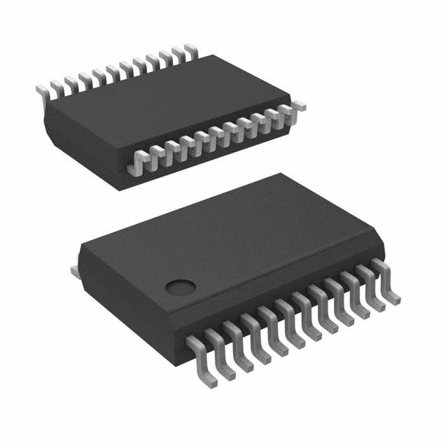
| 产品图片 |
|
| rohs | 符合RoHS无铅 / 符合限制有害物质指令(RoHS)规范要求 |
| 产品系列 | 放大器 IC,差分放大器,Analog Devices AD604ARSZX-AMP® |
| 数据手册 | |
| 产品型号 | AD604ARSZ |
| 产品培训模块 | http://www.digikey.cn/PTM/IndividualPTM.page?site=cn&lang=zhs&ptm=30008http://www.digikey.cn/PTM/IndividualPTM.page?site=cn&lang=zhs&ptm=26202 |
| 产品目录页面 | |
| 产品种类 | 差分放大器 |
| 供应商器件封装 | 24-SSOP |
| 共模抑制比—最小值 | - 20 dB |
| 包装 | 管件 |
| 压摆率 | 170 V/µs |
| 商标 | Analog Devices |
| 增益带宽积 | - |
| 安装类型 | 表面贴装 |
| 安装风格 | SMD/SMT |
| 封装 | Tube |
| 封装/外壳 | 24-SSOP(0.209",5.30mm 宽) |
| 封装/箱体 | SSOP-24 |
| 工作温度 | -40°C ~ 85°C |
| 工作电源电压 | 5 V |
| 工厂包装数量 | 59 |
| 带宽 | 40 MHz |
| 放大器类型 | 可变增益 |
| 最大功率耗散 | 1.1 W |
| 最大双重电源电压 | 5 V |
| 最大工作温度 | + 85 C |
| 最大输入电阻 | 300 kOhms |
| 最小工作温度 | - 40 C |
| 标准包装 | 1 |
| 电压-电源,单/双 (±) | - |
| 电压-输入失调 | - |
| 电流-电源 | 32mA |
| 电流-输入偏置 | 400nA |
| 电流-输出/通道 | 40mA |
| 电源电流 | 32 mA |
| 电路数 | 2 |
| 系列 | AD604 |
| 视频文件 | http://www.digikey.cn/classic/video.aspx?PlayerID=1364138032001&width=640&height=505&videoID=2245193153001http://www.digikey.cn/classic/video.aspx?PlayerID=1364138032001&width=640&height=505&videoID=2245193159001 |
| 转换速度 | 170 V/us |
| 输出类型 | - |
| 通道数量 | 2 Channel |
| 配用 | /product-detail/zh/AD604-EVALZ/AD604-EVALZ-ND/1769813 |


- 商务部:美国ITC正式对集成电路等产品启动337调查
- 曝三星4nm工艺存在良率问题 高通将骁龙8 Gen1或转产台积电
- 太阳诱电将投资9.5亿元在常州建新厂生产MLCC 预计2023年完工
- 英特尔发布欧洲新工厂建设计划 深化IDM 2.0 战略
- 台积电先进制程称霸业界 有大客户加持明年业绩稳了
- 达到5530亿美元!SIA预计今年全球半导体销售额将创下新高
- 英特尔拟将自动驾驶子公司Mobileye上市 估值或超500亿美元
- 三星加码芯片和SET,合并消费电子和移动部门,撤换高东真等 CEO
- 三星电子宣布重大人事变动 还合并消费电子和移动部门
- 海关总署:前11个月进口集成电路产品价值2.52万亿元 增长14.8%


PDF Datasheet 数据手册内容提取
Dual, Ultralow Noise Variable Gain Amplifier AD604 FEATURES FUNCTIONAL BLOCK DIAGRAM Ultralow input noise at maximum gain PAOx FBKx –DSXx +DSXx VGNx 0.80 nV/√Hz, 3.0 pA/√Hz 2 independent linear-in-dB channels AD604 GAANIND CSCOANLTIRNOGL VREF Absolute gain range per channel programmable 0dB TO –48.4dB 0 dB to 48 dB (preamplifier gain = 14 dB) through 6 dB to DIFFERENTIAL PASSIVE INPUT 54 dB (preamplifier gain = 20 dB) PAIx ATTENUATOR AFA OUTx ±1.0 dB gain accuracy R-1.5R 40Ω LADDER Bandwidth: 40 MHz (−3 dB) NETWORK VOCM Input resistance: 300 kΩ 32Ω FIXED GAIN AMPLIFIER Variable gain scaling: 20 dB/V through 40 dB/V 34.4dB 8Ω SStinagbllee- geanidne wdi uthn itpeomlapre graatiunr ceo anntdro slu pply variations COMx 00540-001 Power shutdown at lower end of gain control Figure 1. Drive ADCs directly APPLICATIONS Ultrasound and sonar time-gain controls High performance AGC systems Signal measurement GENERAL DESCRIPTION The AD604 is an ultralow noise, very accurate, dual-channel, Preamplifier gains between 5 and 10 (14 dB and 20 dB) provide linear-in-dB variable gain amplifier (VGA) optimized for time- overall gain ranges per channel of 0 dB through 48 dB and 6 dB based variable gain control in ultrasound applications; however, through 54 dB. The two channels of the AD604 can be cascaded it supports any application requiring low noise, wide bandwidth, to provide greater levels of gain range by bypassing the preamplifier variable gain control. Each channel of the AD604 provides a of the second channel. However, in multiple channel systems, 300 kΩ input resistance and unipolar gain control for ease of cascading the AD604 with other devices in the AD60x VGA use. User-determined gain ranges, gain scaling (dB/V), and dc family that do not include a preamplifier may provide a more level shifting of output further optimize performance. efficient solution. The AD604 provides access to the output of the preamplifier, allowing for external filtering between the Each channel of the AD604 uses a high performance preamplifier and the differential attenuator stage. preamplifier that provides an input-referred noise voltage of 0.8 nV/√Hz. The very accurate linear-in-dB response of the Note that scale factors up to 40 dB/V are achievable with reduced AD604 is achieved with the differential input exponential accuracy for scales above 30 dB/V. The gain scales linearly in amplifier (DSX-AMP) architecture. Each DSX-AMP comprises decibels with control voltages of 0.4 V to 2.4 V with the 20 dB/V a variable attenuator of 0 dB to 48.36 dB followed by a high scale. Below and above this gain control range, the gain begins speed fixed-gain amplifier. The attenuator is a 7-stage to deviate from the ideal linear-in-dB control law. The gain R-1.5R ladder network. The attenuation between tap points is control region below 0.1 V is not used for gain control. When 6.908 dB and 48.36 dB for the ladder network. the gain control voltage is <50 mV, the amplifier channel is powered down to 1.9 mA. The equation for the linear-in-dB gain response is The AD604 is available in 24-lead SSOP, SOIC, and PDIP G (dB) = packages and is guaranteed for operation over the −40°C to (Gain Scaling (dB/V) × VGN (V)) + (Preamp Gain (dB) – 19 dB) +85°C temperature range. Rev. G Information furnished by Analog Devices is believed to be accurate and reliable. However, no responsibility is assumed by Analog Devices for its use, nor for any infringements of patents or other One Technology Way, P.O. Box 9106, Norwood, MA 02062-9106, U.S.A. rights of third parties that may result from its use. Specifications subject to change without notice. No license is granted by implication or otherwise under any patent or patent rights of Analog Devices. Tel: 781.329.4700 www.analog.com Trademarks and registered trademarks are the property of their respective owners. Fax: 781.461.3113 ©1996–2010 Analog Devices, Inc. All rights reserved.
AD604 TABLE OF CONTENTS Features .............................................................................................. 1 Applications Information .............................................................. 18 Applications ....................................................................................... 1 Ultralow Noise AGC Amplifier with 82 dB to 96 dB Gain Functional Block Diagram .............................................................. 1 Range ............................................................................................ 19 General Description ......................................................................... 1 Ultralow Noise, Differential Input-Differential Output VGA ....................................................................................................... 21 Revision History ............................................................................... 2 Medical Ultrasound TGC Driving the AD9050, a 10-Bit, 40 Specifications ..................................................................................... 3 MSPS ADC .................................................................................. 22 Absolute Maximum Ratings ............................................................ 5 Evaluation Board ............................................................................ 24 ESD Caution .................................................................................. 5 Connecting a Waveform to the AD604-EVALZ ........................ 24 Pin Configuration and Function Descriptions ............................. 6 DSX Input Connections ............................................................ 24 Typical Performance Characteristics ............................................. 7 Preamplifier Gain ....................................................................... 25 Theory of Operation ...................................................................... 13 Outputs ........................................................................................ 25 Preamplifier ................................................................................. 14 DC Operating Conditions ......................................................... 25 Differential Ladder (Attenuator) .............................................. 15 Evaluation Board Artwork and Schematic ............................. 26 AC Coupling ............................................................................... 16 Outline Dimensions ....................................................................... 28 Gain Control Interface ............................................................... 16 Ordering Guide .......................................................................... 29 Active Feedback Amplifier (Fixed-Gain Amp) ...................... 16 REVISION HISTORY 12/10—Rev. F to Rev. G Changes to An Ultralow Noise AGC Amplifier with 82 dB to Changes to Figure 1 .......................................................................... 1 96 dB Gain Range Section ............................................................. 19 Changes to Evaluation Board Section, Figure 55, Using the Changes to Figure 55 and Figure 56............................................. 24 Preamplifier Section, Figure 56, and DSX Input Connections Changes to Cascaded DSX Section and Outputs Section ......... 25 Section .............................................................................................. 24 Changes to Figure 57 to Figure 60 ................................................ 26 Changes to Preamplifier Gain Section, Outputs Section, DC Changes to Figure 61 and Table 6................................................. 27 Operating Conditions Section, Table 4 and Table 5................... 25 Changes to Ordering Guide .......................................................... 29 Added Figure 57; Renumbered Sequentially .............................. 25 3/07—Rev. B to Rev. C Changes to Figure 58 to Figure 61 ................................................ 26 Added Evaluation Board Section ................................................. 24 Added Figure 62 .............................................................................. 26 Added Evaluation Board Artwork and Schematics Section ..... 26 Changes to Figure 63 ...................................................................... 27 Changes to Ordering Guide .......................................................... 29 Updated Outline Dimensions ....................................................... 28 12/06—Rev. A to Rev. B 4/10—Rev. E to Rev. F Changes to General Description .....................................................1 Changes to Figure 55, DSX Input Connections Section, and Changes to Figure 54 ...................................................................... 23 Differential DSX Inputs Section ................................................... 24 Changes to Ordering Guide .......................................................... 25 Changes to Figure 61, Deleted Table 6 ......................................... 27 1/04—Rev. 0 to Rev. A Changes to Ordering Guide .......................................................... 29 Changes to Specifications .................................................................2 10/08—Rev. D to Rev. E Changes to Absolute Maximum Ratings ........................................3 Changes to Figure 1 .......................................................................... 1 Changes to Ordering Guide .............................................................3 Changes to Figure 37 ...................................................................... 13 Changes to Figure 1 Caption............................................................5 Changes to Figure 41 ...................................................................... 15 Changes to Figure 11 Caption .........................................................6 Changes to Evaluation Board Model Name ................................ 24 Changes to Figure 17 .........................................................................6 Changes to Ordering Guide .......................................................... 29 Changes to Figure 51 ...................................................................... 17 1/08—Rev. C to Rev. D Updated Outline Dimensions ....................................................... 18 Changes to AC Coupling Section ................................................. 16 10/96—Revision 0: Initial Version Changes to Applications Information Section ............................ 18 Rev. G | Page 2 of 32
AD604 SPECIFICATIONS Each amplifier channel at T = 25°C, V = ±5 V, R = 50 Ω, R = 500 Ω, C = 5 pF, V = 2.50 V (scaling = 20 dB/V), 0 dB to 48 dB gain A S S L L REF range (preamplifier gain = 14 dB), VOCM = 2.5 V, C1 and C2 = 0.1 μF (see Figure 37), unless otherwise noted. Table 1. Parameter Conditions Min Typ Max Unit INPUT CHARACTERISTICS Preamplifier Input Resistance 300 kΩ Input Capacitance 8.5 pF Input Bias Current −27 mA Peak Input Voltage Preamplifier gain = 14 dB ±400 mV Preamplifier gain = 20 dB ±200 mV Input Voltage Noise VGN = 2.9 V, R = 0 Ω S Preamplifier gain = 14 dB 0.8 nV/√Hz Preamplifier gain = 20 dB 0.73 nV/√Hz Input Current Noise Independent of gain 3.0 pA/√Hz Noise Figure R = 50 Ω, f = 10 MHz, VGN = 2.9 V 2.3 dB S R = 200 Ω, f = 10 MHz, VGN = 2.9 V 1.1 dB S DSX Input Resistance 175 Ω Input Capacitance 3.0 pF Peak Input Voltage 2.5 ± 2 V Input Voltage Noise VGN = 2.9 V 1.8 nV/√Hz Input Current Noise VGN = 2.9 V 2.7 pA/√Hz Noise Figure R = 50 Ω, f = 10 MHz, VGN = 2.9 V 8.4 dB S R = 200 Ω, f = 10 MHz, VGN = 2.9 V 12 dB S Common-Mode Rejection Ratio f = 1 MHz, VGN = 2.65 V −20 dB OUTPUT CHARACTERISTICS −3 dB Bandwidth Constant with gain 40 MHz Slew Rate VGN = 1.5 V, output = 1 V step 170 V/μs Output Signal Range R ≥ 500 Ω 2.5 ± 1.5 V L Output Impedance f = 10 MHz 2 Ω Output Short-Circuit Current ±40 mA Harmonic Distortion VGN = 1 V, V = 1 V p-p OUT HD2 f = 1 MHz −54 dBc HD3 f = 1 MHz −67 dBc HD2 f = 10 MHz −43 dBc HD3 f = 10 MHz −48 dBc Two-Tone Intermodulation Distortion (IMD) VGN = 2.9 V, V = 1 V p-p OUT f = 1 MHz −74 dBc f = 10 MHz −71 dBc Third-Order Intercept f = 10 MHz, VGN = 2.65 V, V = 1 V p-p, −12.5 dBm OUT input referred 1 dB Compression Point f = 1 MHz, VGN = 2.9 V, output referred 15 dBm Channel-to-Channel Crosstalk V = 1 V p-p, f = 1 MHz, −30 dB OUT Channel 1: VGN = 2.65 V, inputs shorted, Channel 2: VGN = 1.5 V (mid gain) Group Delay Variation 1 MHz < f < 10 MHz, full gain range ±2 ns VOCM Input Resistance 45 kΩ Rev. G | Page 3 of 32
AD604 Parameter Conditions Min Typ Max Unit ACCURACY Absolute Gain Error 0 dB to 3 dB 0.25 V < VGN < 0.400 V −1.2 +0.75 +3 dB 3 dB to 43 dB 0.400 V < VGN < 2.400 V −1.0 ±0.3 +1.0 dB 43 dB to 48 dB 2.400 V < VGN < 2.65 V −3.5 −1.25 +1.2 dB Gain Scaling Error 0.400 V < VGN < 2.400 V ±0.25 dB/V Output Offset Voltage VREF = 2.500 V, VOCM = 2.500 V −50 ±30 +50 mV Output Offset Variation VREF = 2.500 V, VOCM = 2.500 V 30 50 mV GAIN CONTROL INTERFACE Gain Scaling Factor VREF = 2.5 V, 0.4 V < VGN < 2.4 V 19 20 21 dB/V VREF = 1.67 V 30 dB/V Gain Range Preamplifier gain = 14 dB 0 to 48 dB Preamplifier gain = 20 dB 6 to 54 dB Input Voltage (VGN) Range 20 dB/V, VREF = 2.5 V 0.1 to 2.9 V Input Bias Current −0.4 μA Input Resistance 2 MΩ Response Time 48 dB gain change 0.2 μs VREF Input Resistance 10 kΩ POWER SUPPLY Specified Operating Range One complete channel ±5 V One DSX only 5 V Power Dissipation One complete channel 220 mW One DSX only 95 mW Quiescent Supply Current VPOS, one complete channel 32 36 mA VPOS, one DSX only 19 23 mA VNEG, one preamplifier only −15 −12 mA Powered Down VPOS, VGN < 50 mV, one channel 1.9 3.0 mA VNEG, VGN < 50 mV, one channel −150 μA Power-Up Response Time 48 dB gain change, V = 2 V p-p 0.6 μs OUT Power-Down Response Time 0.4 μs Rev. G | Page 4 of 32
AD604 ABSOLUTE MAXIMUM RATINGS Stresses above those listed under Absolute Maximum Ratings Table 2. may cause permanent damage to the device. This is a stress Parameter1, 2 Rating rating only; functional operation of the device at these or any Supply Voltage ±VS other conditions above those indicated in the operational Pin 17 to Pin 20 (with Pin 16, Pin 22 = 0 V) ±6.5 V section of this specification is not implied. Exposure to absolute Input Voltages maximum rating conditions for extended periods may affect Pin 1, Pin 2, Pin 11, Pin 12 VPOS/2 ± 2 V device reliability. continuous Pin 4, Pin 9 ±2 V ESD CAUTION Pin 5, Pin 8 VPOS, VNEG Pin 6, Pin 7, Pin 13, Pin 14, Pin 23, Pin 24 VPOS, 0 V Internal Power Dissipation PDIP (N) 2.2 W SOIC (RW) 1.7 W SSOP (RS) 1.1 W Operating Temperature Range −40°C to +85°C Storage Temperature Range −65°C to +150°C Lead Temperature, Soldering 60 sec 300°C θJA3 AD604AN 105°C/W AD604AR 73°C/W AD604ARS 112°C/W θJC3 AD604AN 35°C/W AD604AR 38°C/W AD604ARS 34°C/W 1 Pin 1, Pin 2, Pin 11 to Pin 14, Pin 23, and Pin 24 are part of a single-supply circuit. The part is likely to suffer damage if any of these pins are accidentally connected to VN. 2 When driven from an external low impedance source. 3 Using MIL-STD-883 test method G43-87 with a 1S (2-layer) test board. Rev. G | Page 5 of 32
AD604 PIN CONFIGURATION AND FUNCTION DESCRIPTIONS –DSX1 1 24 VGN1 +DSX1 2 23 VREF PAO1 3 22 OUT1 FBK1 4 21 GND1 PAI1 5 20 VPOS AD604 COM1 6 19 VNEG TOPVIEW COM2 7 (NottoScale) 18 VNEG PAI2 8 17 VPOS FBK2 9 16 GND2 PAO2 10 15 OUT2 +–DDSSXX22 1112 1143 VVOGCNM2 00540-002 Figure 2. Pin Configuration Table 3. Pin Function Descriptions Pin No. Mnemonic Description 1 –DSX1 Channel 1 Negative Signal Input to DSX1. 2 +DSX1 Channel 1 Positive Signal Input to DSX1. 3 PAO1 Channel 1 Preamplifier Output. 4 FBK1 Channel 1 Preamplifier Feedback Pin. 5 PAI1 Channel 1 Preamplifier Positive Input. 6 COM1 Channel 1 Signal Ground. When this pin is connected to positive supply, Preamplifier 1 shuts down. 7 COM2 Channel 2 Signal Ground. When this pin is connected to positive supply, Preamplifier 2 shuts down. 8 PAI2 Channel 2 Preamplifier Positive Input. 9 FBK2 Channel 2 Preamplifier Feedback Pin. 10 PAO2 Channel 2 Preamplifier Output. 11 +DSX2 Channel 2 Positive Signal Input to DSX2. 12 –DSX2 Channel 2 Negative Signal Input to DSX2. 13 VGN2 Channel 2 Gain Control Input and Power-Down Pin. If this pin is grounded, the device is off; otherwise, positive voltage increases gain. 14 VOCM Input to this pin defines the common mode of the output at OUT1 and OUT2. 15 OUT2 Channel 2 Signal Output. 16 GND2 Ground. 17 VPOS Positive Supply. 18 VNEG Negative Supply. 19 VNEG Negative Supply. 20 VPOS Positive Supply. 21 GND1 Ground. 22 OUT1 Channel 1 Signal Output. 23 VREF Input to this pin sets gain scaling for both channels to 2.5 V = 20 dB/V and 1.67 V = 30 dB/V. 24 VGN1 Channel 1 Gain Control Input and Power-Down Pin. If this pin is grounded, the device is off; otherwise, positive voltage increases gain. Rev. G | Page 6 of 32
AD604 TYPICAL PERFORMANCE CHARACTERISTICS Unless otherwise noted, G (preamplifier) = 14 dB, VREF = 2.5 V (20 dB/V scaling), f = 1 MHz, R = 500 Ω, C = 5 pF, T = 25°C, and L L A V = ±5 V. SS 50 40.0 37.5 40 THEORETICAL 3 CURVES –40°C, 35.0 +25°C, V) 30 +85°C B/ d 32.5 B) G ( ACTUAL d N AIN ( 20 CALI 30.0 G S N 27.5 10 AI G 25.0 0 –10 00540-003 2202..05 00540-006 0.1 0.5 0.9 1.3 1.7 2.1 2.5 2.9 1.25 1.50 1.75 2.00 2.25 2.50 VGN (V) VREF(V) Figure 3. Gain vs. VGN for Three Temperatures Figure 6. Gain Scaling vs. VREF 60 2.0 50 G(0d(PBRTEOAM+4P8)d=B+)14dB 1.5 40 1.0 30 G(PREAMP)=+20dB dB) 0.5 B) (+6dBTO+54dB) R ( –40°C +25°C d O N ( 20 RR 0 AI E G N 10 DSX ONLY GAI –0.5 +85°C (–14dBTO+34dB) 0 –1.0 ––1200 00540-004 ––12..50 00540-007 0.1 0.5 0.9 1.3 1.7 2.1 2.5 2.9 0.2 0.7 1.2 1.7 2.2 2.7 VGN(V) VGN(V) Figure 4. Gain vs. VGN for Different Preamplifier Gains Figure 7. Gain Error vs. VGN 50 2.0 ACTUAL 1.5 40 ACTUAL 30dB/V 1.0 VREF=1.67V 30 B) d 0.5 FREQ=1MHz B) R ( d O AIN ( 20 ERR 0 G N 20dB/V AI –0.5 10 VREF=2.5V G FREQ=10MHz FREQ=5MHz –1.0 0 –10 00540-005 ––12..50 00540-008 0.1 0.5 0.9 1.3 1.7 2.1 2.5 2.9 0.2 0.7 1.2 1.7 2.2 2.7 VGN(V) VGN(V) Figure 5. Gain vs. VGN for Different Gain Scalings Figure 8. Gain Error vs. VGN at Different Frequencies Rev. G | Page 7 of 32
AD604 2.0 50 40 VGN=2.5V 1.5 VGN=2.9V 30 1.0 20 VGN=1.5V B) 20dB/V R (d 0.5 VREF=2.5V B) 10 VGN=0.5V O d ERR 0 AIN ( 0 VGN=0.1V N G –10 AI –0.5 G 30dB/V VREF=1.67V –20 –1.0 –30 VGN=0V ––12..50 00540-009 ––5400 00540-012 0.2 0.7 1.2 1.7 2.2 2.7 100k 1M 10M 100M VGN(V) FREQUENCY(Hz) Figure 9. Gain Error vs. VGN for Two Gain Scaling Values Figure 12. AC Response for Various Values of VGN 25 2.55 N=50 VOCM=2.5V VGN1=1.0V VGN2=1.0V 2.54 ΔG(dB)= –40°C 20 G(CH1)– G(CH2) 2.53 2.52 E G 15 2.51 CENTA (V)OUT 2.50 +25°C R V E 10 2.49 P 2.48 5 2.47 +85°C 0 00540-010 22..4456 00540-013 –1.0 –0.8 –0.6 –0.4 –0.2 0.1 0.3 0.5 0.7 0.9 0.2 0.7 1.2 1.7 2.2 2.7 DELTA GAIN(dB) VGN(V) Figure 10. Gain Match; VGN1 = VGN2 = 1.0 V Figure 13. Output Offset vs. VGN for Three Temperatures 25 210 N=50 VGN1=2.50V VGN2=2.50V ΔG(dB)= 190 20 G(CH1)– G(CH2) 170 GE 15 Hz) TA V/ CEN E (n 150 ER 10 OIS +85°C P N 130 5 +25°C 110 0 00540-011 90 –40°C 00540-014 –1.0 –0.8 –0.6 –0.4 –0.2 0.1 0.3 0.5 0.7 0.9 0.1 0.5 0.9 1.3 1.7 2.1 2.5 2.9 DELTA GAIN(dB) VGN(V) Figure 11. Gain Match; VGN1 = VGN2 = 2.50 V Figure 14. Output Referred Noise vs. VGN for Three Temperatures Rev. G | Page 8 of 32
AD604 1000 10 VGN=2.9V 100 Hz) Hz) V/ V/ E (n 10 E (n 1 S S OI OI N N 1 RSOURCEALONE 0.1 00540-015 0.1 00540-018 0.1 0.5 0.9 1.3 1.7 2.1 2.5 2.9 1 10 100 1k VGN(V) RSOURCE(Ω) Figure 15. Input Referred Noise vs. VGN Figure 18. Input Referred Noise vs. RSOURCE 900 16 VGN=2.9V VGN=2.9V 15 14 850 13 12 800 B) 11 Hz) E (d 10 E (pV/ 750 FIGUR 98 OIS SE 7 N 700 NOI 6 5 4 650 600 00540-016 321 00540-019 –40 –20 0 20 40 60 80 90 1 10 100 1k 10k TEMPERATURE(°C) RSOURCE(Ω) Figure 16. Input Referred Noise vs. Temperature Figure 19. Noise Figure vs. RSOURCE 770 40 VGN=2.9V RS=240Ω 35 765 30 760 B) Hz) E (d 25 NOISE (pV/ 775505 OISE FIGUR 2105 N 10 745 740 00540-017 05 00540-020 100k 1M 10M 0 0.4 0.8 1.2 1.6 2.0 2.4 2.8 FREQUENCY(Hz) VGN(V) Figure 17. Input Referred Noise vs. Frequency Figure 20. Noise Figure vs. VGN Rev. G | Page 9 of 32
AD604 –40 –20 VO=1Vp-p VO=1Vp-p VGN=1V –30 VGN=1V –45 c) –40 B d N ( –50 –50 O RTI m) –60 O HD2 B DIST –55 (dUT –70 C HD3 PO –80 NI O –60 M –90 R A H –100 –65 –70 00540-021 ––111200 00540-024 100k 1M 10M 100M 9.96 9.98 10.00 10.02 10.04 FREQUENCY(Hz) FREQUENCY(MHz) Figure 21. Harmonic Distortion vs. Frequency Figure 24. Intermodulation Distortion –30 5 VO=1Vp-p –35 0 c) –40 INPUT B HD2(10MHz) –5 SIGNAL N (d –45 L80IM0mITVp-p TIO –50 –10 10MHz DISTOR –55 HD3(10MHz) (dBm)N –15 C –60 PI NI –20 1MHz O M –65 AR –25 H –70 HD2(1MHz) ––7850 HD3(1MHz) 00540-022 ––3305 00540-025 0.5 0.9 1.3 1.7 2.1 2.5 2.9 0.1 0.5 0.9 1.3 1.7 2.1 2.5 2.9 VGN(V) VGN(V) Figure 22. Harmonic Distortion vs. VGN Figure 25. 1 dB Compression vs. VGN –20 25 RS VO=1Vp-p VO=1Vp-p DUT VGN=1V –30 50Ω 500Ω 20 c) N (dB –40 HD2(10MHz) 15 f=1MHz O TI 10 STOR –50 HD3(10MHz) dBm) 5 DI 3 ( NIC HD2(1MHz) IP 0 f=10MHz O –60 M AR HD3(1MHz) –5 H –70 –80 00540-023 ––1150 00540-026 0 50 100 150 200 250 0.4 0.9 1.4 1.9 2.4 2.9 RSOURCE(Ω) VGN(V) Figure 23. Harmonic Distortion vs. RSOURCE Figure 26. Third-Order Intercept vs. VGN Rev. G | Page 10 of 32
AD604 2V VO=2Vp-p VGN=1.5V 500mV 2.9V 100 90 V/DIV N (V) m G 00 V 4 10 0% 0.1V –2V 00540-027 500mV 100ns 00540-030 253ns 100ns/DIV 1.253µs Figure 27. Large Signal Pulse Response Figure 30. Gain Response 200 0 VO=200mVp-p VGN1=1V VGN=1.5V VOUT1=1Vp-p –10 VIN2= GND –20 B) VGN2=2.9V d V K ( –30 V/DI TAL 0m SS –40 VGN2=2V 4 O R C –50 TRIG'D VGN2=1.5V –60 VGN2=0.1V –200 00540-028 –70 00540-031 253ns 100ns/DIV 1.253µs 100k 1M 10M 100M FREQUENCY(Hz) Figure 28. Small Signal Pulse Response Figure 31. Crosstalk (Channel 1 to Channel 2) vs. Frequency 0 500mV –10 2.9V 100 VGN=2.9V 90 –20 V) B) VGN ( MRR (d –30 VGN=2.5V C VGN=2V –40 10 0% 0V 500mV 200ns 00540-029 ––5600 VGN=0.1V 00540-032 100k 1M 10M 100M FREQUENCY(Hz) Figure 29. Power-Up/Power-Down Response Figure 32. DSX Common-Mode Rejection Ratio vs. Frequency Rev. G | Page 11 of 32
AD604 1M 40 +IS(AD604)=+IS(PA)++IS(DSX) –IS(AD604)=–IS(PA) 35 100k T IMPEDANCE (Ω) 101kk LY CURRENT (mA) 23210055 DSX(+IS) AD604(+IS) PU 100 PP N U I S 10 101 00540-033 05 +IS(VGN=0) PREAMP(±IS) 00540-035 1k 10k 100k 1M 10M 100M –40 –20 0 20 40 60 80 90 FREQUENCY(Hz) TEMPERATURE(°C) Figure 33. Input Impedance vs. Frequency Figure 35. Supply Current (One Channel) vs. Temperature 27.6 20 27.4 18 27.2 A) µ 16 T ( 27.0 N AS CURRE 2266..86 ELAY (ns) 1142 VGN=0.1V BI D T 26.4 U P 10 N I 26.2 VGN=2.9V 8 2256..80 00540-034 6 00540-036 –40 –20 0 20 40 60 80 90 100k 1M 10M 100M TEMPERATURE(°C) FREQUENCY(Hz) Figure 34. Input Bias Current vs. Temperature Figure 36. Group Delay vs. Frequency Rev. G | Page 12 of 32
AD604 THEORY OF OPERATION The AD604 is a dual-channel VGA with an ultralow noise example, if the preamp gain is set to 14 dB and VREF is set to preamplifier. Figure 37 shows the simplified block diagram of 2.50 V (to establish a gain scaling of 20 dB/V), the gain equation one channel. Each identical channel consists of a preamplifier simplifies to with gain setting resistors (R5, R6, and R7) and a single-supply G (dB) = 20 (dB/V) × VGN (V) – 5 dB X-AMP® (hereafter called DSX, differential single-supply X-AMP) The desired gain can then be achieved by setting the unipolar made up of the following: gain control (VGN) to a voltage within its nominal operating • A precision passive attenuator (differential ladder). range of 0.25 V to 2.65 V (for 20 dB/V gain scaling). The gain is • A gain control block. monotonic for a complete gain control voltage range of 0.1 V to 2.9 V. Maximum gain can be achieved at a VGN of 2.9 V. • A VOCM buffer with supply splitting resistors (R3 and R4). The inputs VREF and VOCM are common to both channels. They are decoupled to ground, minimizing interchannel • An active feedback amplifier (AFA) with gain setting crosstalk. For the highest gain scaling accuracy, VREF should resistors (R1 and R2). To understand the active-feedback have an external low impedance voltage source. For low accuracy amplifier topology, refer to the AD830 data sheet. The 20 dB/V applications, the VREF input can be decoupled with a AD830 is a practical implementation of the idea. capacitor to ground. In this mode, the gain scaling is determined The preamplifier is powered by a ±5 V supply, while the DSX by the midpoint between VPOS and GND; therefore, care uses a single +5 V supply. The linear-in-dB gain response of the should be taken to control the supply voltage to 5 V. The input AD604 can generally be described by resistance looking into the VREF pin is 10 kΩ ± 20%. G (dB) = Gain Scaling (dB/V) × Gain Control (V) + The DSX portion of the AD604 is a single-supply circuit, and (Preamp Gain (dB) − 19 dB) (1) the VOCM pin is used to establish the dc level of the midpoint of this portion of the circuit. The VOCM pin only needs an Each channel provides between 0 dB to 48.4 dB and 6 dB to 54.4 external decoupling capacitor to ground to center the midpoint dB of gain, depending on the user-determined preamplifier between the supply voltages (5 V, GND); however, the VOCM gain. The center 40 dB of gain is exactly linear-in-dB while the can be adjusted to other voltage levels if the dc common-mode gain error increases at the top and bottom of the range. The gain level of the output is important to the user (for example, see the of the preamplifier is typically either 14 dB or 20 dB but can be section entitled Medical Ultrasound TGC Driving the AD9050, set to intermediate values by a single external resistor (see the a 10-Bit, 40 MSPS ADC). The input resistance looking into the Preamplifier section for details). The gain of the DSX can vary VOCM pin is 45 kΩ ± 20%. from −14 dB to +34.4 dB, as determined by the gain control voltage (VGN). The VREF input establishes the gain scaling; the useful gain scaling range is between 20 dB/V and 40 dB/V for a VREF voltage of 2.5 V and 1.25 V, respectively. For VREF GAIN VGNx CONTROL 175Ω PAIx PAOx C1 +DSXx R7 DISTRIBUTED GM 40Ω EXT. DIFFERENTIAL G1 FBKx C2 –DSXx ATTENUATOR R5 32Ω Ao OUTx 175Ω VPOS R6 8Ω G2 R3 200kΩ COMx R2 R1 VOCM 20Ω 820Ω C3 R4 EXT. 200kΩ 00540-037 Figure 37. Simplified Block Diagram of a Single Channel of the AD604 Rev. G | Page 13 of 32
AD604 PREAMPLIFIER preamplifier to be 17.7 dB. The −3 dB small signal bandwidth of one complete channel of the AD604 (preamplifier and DSX) is The input capability of the following single-supply DSX (2.5 ± 2 V 40 MHz and is independent of gain. for a +5 V supply) limits the maximum input voltage of the preamplifier to ±400 mV for the 14 dB gain configuration or To achieve optimum specifications, power and ground manage- ±200 mV for the 20 dB gain configuration. ment are critical to the AD604. Large dynamic currents result because of the low resistances needed for the desired noise The preamplifier gain can be programmed to 14 dB or 20 dB by performance. Most of the difficulty is with the very low gain either shorting the FBK1 node to PAO1 (14 dB) or by leaving setting resistors of the preamplifier that allow for a total input the FBK1 node open (20 dB). These two gain settings are very referred noise, including the DSX, as low as 0.8 nV/√Hz. The accurate because they are set by the ratio of the on-chip resistors. consequently large dynamic currents have to be carefully Any intermediate gain can be achieved by connecting the handled to maintain performance even at large signal levels. appropriate resistor value between PAO1 and FBK1 according to Equation 2 and Equation 3. 20 OPEN ( ) 19 V R7||R +R5+R6 G= OUT = EXT (2) 18 40Ω V R6 IN 17 R = [R6×G −(R5+ R6)]×R7 (3) B) 16 EXT R7 −(R6×G)+(R5+ R6) N (d 15 AI SHORT Because the internal resistors have an absolute tolerance of ±20%, G 14 IN the gain can be in error by as much as 0.33 dB when REXT is 30 Ω, 13 VIN 150Ω where it is assumed that REXT is exact. 12 508ΩΩ 32Ω 40Ω REXT F17ig.5u rdeB 3, 8a nshdo 2w0s d hBo.w T hthee g parinea rmanpglief ioefr ais s sinetg tleo cghaainnsn oelf o1f4 t dhBe , 1101 00540-039 100k 1M 10M 100M AD604 is 0 dB to 48 dB when the preamplifier is set to 14 dB FREQUENCY(Hz) (Figure 38a), 3.5 dB to 51.5 dB for a preamp gain of 17.5 dB Figure 39. AC Response for Preamplifier Gains of 14 dB, 17.5 dB, and 20 dB (Figure 38b), and 6 dB to 54 dB for the highest preamp gain of The preamplifier uses a dual ±5 V supply to accommodate large 20 dB (Figure 38c). dynamic currents and a ground referenced input. The preamplifier PAI1 output is also ground referenced and requires a common-mode PAO1 level shift into the single-supply DSX. The two external coupling R7 R6 R5 40Ω capacitors (C1 and C2 in Figure 37) connected to the PAO1 and 8Ω 32Ω COM1 FBK1 +DSXx, and –DSXx, nodes and ground, respectively, perform this function (see the AC Coupling section). In addition, they a.PREAMP GAIN=14dB eliminate any offset that would otherwise be introduced by the preamplifier. It should be noted that an offset of 1 mV at the PAI1 PAO1 input of the DSX is amplified by 34.4 dB (× 52.5) when the gain R7 R10 control voltage is at its maximum; this equates to 52.5 mV at the R6 R5 40Ω 40Ω 8Ω 32Ω output. AC coupling is consequently required to keep the offset COM1 FBK1 from degrading the output signal range. b.PREAMP GAIN=17.5dB The gain-setting preamplifier feedback resistors are small enough (8 Ω and 32 Ω) that even an additional 1 Ω in the PAI1 ground connection at Pin COM1 (the input common-mode PAO1 R7 reference) seriously degrades gain accuracy and noise performance. R6 R5 40Ω 8Ω 32Ω This node is sensitive, and careful attention is necessary to COM1 FBK1 c.PREAMP GAIN=20dB 00540-038 mnoidneim shizoeu tlhde b ger aosu snhdo irmt apse pdoansscieb.l eA. ll connections to the COM1 Figure 38. Preamplifier Gain Programmability The preamplifier, including the gain setting resistors, has a For a preamplifier gain of 14 dB, the −3 dB small signal bandwidth noise performance of 0.71 nV/√Hz and 3 pA/√Hz. Note that a of the preamplifier is 130 MHz. When the gain is at its maximum significant portion of the total input referred voltage noise is of 20 dB, the bandwidth is reduced by half to 65 MHz. Figure 39 due to the feedback resistors. The equivalent noise resistance shows the ac response for the three preamp gains shown in presented by R5 and R6 in parallel is nominally 6.4 Ω, which Figure 38. Note that the gain for an R of 40 Ω should be contributes 0.33 nV/√Hz to the total input referred voltage noise. EXT 17.5 dB, but the mismatch between the internal resistors and the external resistor causes the actual gain for this particular Rev. G | Page 14 of 32
AD604 The larger portion of the input referred voltage noise comes A unique circuit technique is used to interpolate continuously from the amplifier with 0.63 nV/√Hz. The current noise is among the tap points, thereby providing continuous attenuation independent of gain and depends only on the bias current in from 0 dB to −48.36 dB. The ladder network, together with the the input stage of the preamplifier, which is 3 pA/√Hz. interpolation mechanism, can be considered a voltage-controlled potentiometer. The preamplifier can drive 40 Ω (the nominal feedback resistors) and the following 175 Ω ladder load of the DSX with low Because the DSX circuit uses a single voltage power supply, the distortion. For example, at 10 MHz and 1 V at the output, the input biasing is provided by the VOCM buffer driving the MID preamplifier has less than −45 dB of second and third harmonic node (see Figure 41). Without internal biasing, the user would distortion when driven from a low (25 Ω) source resistance. have to dc bias the inputs externally. If not done carefully, the biasing network can introduce additional noise and offsets. By In applications that require more than 48 dB of gain range, two providing internal biasing, the user is relieved of this task and AD604 channels can be cascaded. Because the preamplifier has only needs to ac-couple the signal into the DSX. Note that the a limited input signal range and consumes over half (120 mW) input to the DSX is still fully differential if driven differentially; of the total power (220 mW), and its ultralow noise is not necessary that is, Pin +DSXx and Pin −DSXx see the same signal but with after the first AD604 channel, a shutdown mechanism that opposite polarity (see the Ultralow Noise, Differential Input- disables only the preamplifier is provided. To shut down the Differential Output VGA section). preamplifier, connect the COM1 pin and/or COM2 pin to the positive supply; the DSX is unaffected. For additional details, What changes is the load seen by the driver; it is 175 Ω when refer to the Applications Information section. each input is driven single-ended but 350 Ω when driven differentially. This is easily explained by thinking of the ladder 1 –DSX1 VGN1 24 network as two 175 Ω resistors connected back-to-back with 2 +DSX1 VREF 23 the middle node, MID, being biased by the VOCM buffer. A 3 PAO1 OUT1 22 differential signal applied between the +DSXx and −DSXx 4 FBK1 GND1 21 nodes results in zero current into the MID node, but a single- 5 PAI1 VPOS 20 ended signal applied to either input, +DSXx or –DSXx, while 6 COM1AD604VNEG 19 the other input is ac-grounded causes the current delivered by 7 COM2 VNEG 18 the source to flow into the VOCM buffer via the MID node. 8 PAI2 VPOS 17 9 FBK2 GND2 16 The ladder resistor value of 175 Ω provides the optimum 10 PAO2 OUT2 15 balance between the load driving capability of the preamplifier 1121 +–DDSSXX22 VVOGCNM2 1134 00540-040 aXn-dA MtheP naorcishei tceocntutrrieb iust tihonat otfh teh oeu rtepsuistt roerfse. rArend a ndoviasne tiasg ceo onfs tthane t Figure 40. Shutdown of Preamplifiers Only vs. gain over most of the gain range. Figure 41 shows that the DIFFERENTIAL LADDER (ATTENUATOR) tap resistance is equal for all taps after only a few taps away from the inputs. The resistance seen looking into each tap is The attenuator before the fixed-gain amplifier of the DSX is 54.4 Ω, which makes 0.95 nV/√Hz of Johnson noise spectral realized by a differential 7-stage R-1.5R resistive ladder network density. Because there are two attenuators, the overall noise with an untrimmed input resistance of 175 Ω single-ended or contribution of the ladder network is √2 times 0.95 nV/√Hz 350 Ω differential. The signal applied at the input of the ladder or 1.34 nV/√Hz, a large fraction of the total DSX noise. The network is attenuated by 6.908 dB per tap; thus, the attenuation balance of the DSX circuit components contributes another at the first tap is 0 dB, at the second, 13.816 dB, and so on, all 1.2 nV/√Hz, which together with the attenuator produces the way to the last tap where the attenuation is 48.356 dB 1.8 nV/√Hz of total DSX input referred noise. (see Figure 41). R –6.908dB R –13.82dB R –20.72dB R –27.63dB R –34.54dB R –41.45dB R –48.36dB +DSXx 1.5R 1.5R 1.5R 1.5R 1.5R 1.5R 1.5R 175Ω MID 1.5R 1.5R 1.5R 1.5R 1.5R 1.5R 1.5R 175Ω R R R R R R R –DSXx N12..O 1RT. 5=ER S9 =6 Ω144Ω 00540-041 Figure 41. R-1.5R Dual Ladder Network Rev. G | Page 15 of 32
AD604 AC COUPLING From these equations, it can be seen that all gain curves intercept at the same −5 dB point; this intercept is +6 dB higher (+1 dB) if The DSX portion of the AD604 is a single-supply circuit and, the preamplifier gain is set to +20 dB or +14 dB lower (−19 dB) therefore, its inputs need to be ac-coupled to accommodate if the preamplifier is not used at all. Outside the central linear ground-based signals. External Capacitors C1 and C2 in Figure 37 range, the gain starts to deviate from the ideal control law but level shift the ground referenced preamplifier output from still provides another 8.4 dB of range. For a given gain scaling, ground to the dc value established by VOCM (nominal 2.5 V). V can be calculated as shown in Equation 7. C1 and C2, together with the 175 Ω looking into each of the REF DSX inputs (+DSXx and −DSXx), act as high-pass filters with 2.500V×20dB/V VREF = (7) corner frequencies depending on the values chosen for C1 and Gain Scale C2. As an example, for values of 0.1 μF at C1 and C2, combined with the 175 Ω input resistance at each side of the differential Usable gain control voltage ranges are 0.1 V to 2.9 V for the ladder of the DSX, the −3 dB high-pass corner is 9.1 kHz. 20 dB/V scale and 0.1 V to 1.45 V for the 40 dB/V scale. VGN voltages of less than 0.1 V are not used for gain control because If the AD604 output needs to be ground referenced, another below 50 mV the channel (preamplifier and DSX) is powered ac coupling capacitor is required for level shifting. This down. This can be used to conserve power and, at the same capacitor also eliminates any dc offsets contributed by the DSX. time, to gate off the signal. The supply current for a powered- With a nominal load of 500 Ω and a 0.1 μF coupling capacitor, down channel is 1.9 mA; the response time to power the device this adds a high-pass filter with −3 dB corner frequency at about on or off is less than 1 μs. 3.2 kHz. ACTIVE FEEDBACK AMPLIFIER (FIXED-GAIN AMP) The choice for all three of these coupling capacitors depends on the application. They should allow the signals of interest to pass To achieve single-supply operation and a fully differential input unattenuated while, at the same time, they can be used to limit to the DSX, an active feedback amplifier (AFA) is used. The the low frequency noise in the system. AFA is an op amp with two gm stages; one of the active stages is used in the feedback path (therefore the name), while the other GAIN CONTROL INTERFACE is used as a differential input. Note that the differential input is The gain control interface provides an input resistance of an open-loop g stage that requires it to be highly linear over m approximately 2 MΩ at VGN1 and gain scaling factors from the expected input signal range. In this design, the g stage that m 20 dB/V to 40 dB/V for VREF input voltages of 2.5 V to 1.25 V, senses the voltages on the attenuator is a distributed one; for respectively. The gain scales linearly in decibels for the center example, there are as many g stages as there are taps on the m 40 dB of gain range, which for VGN is equal to 0.4 V to 2.4 V for ladder network. Only a few of them are on at any one time, the 20 dB/V scale and 0.2 V to 1.2 V for the 40 dB/V scale. Figure 42 depending on the gain control voltage. shows the ideal gain curves for a nominal preamplifier gain The AFA makes a differential input structure possible because of 14 dB, which are described by the following equations: one of its inputs (G1) is fully differential; this input is made up G (20 dB/V) = 20 × VGN – 5, VREF = 2.500 V (4) of a distributed g stage. The second input (G2) is used for m G (20 dB/V) = 30 × VGN – 5, VREF = 1.666 V (5) feedback. The output of G1 is some function of the voltages sensed on the attenuator taps, which is applied to a high-gain G (20 dB/V) = 40 × VGN – 5, VREF = 1.250 V (6) amplifier (A0). Because of negative feedback, the differential input to the high-gain amplifier has to be zero; this in turn 50 implies that the differential input voltage to G2 times g (the m2 45 transconductance of G2) has to be equal to the differential 40 input voltage to G1 times g (the transconductance of G1). m1 35 40dB/V 30dB/V 20dB/V Therefore, the overall gain function of the AFA is 30 B) V g R1+ R2 N (d25 LINEAR-IN-dBRANGE OUT = m1 × (8) GAI20 OPRFEAADM60P4LIWFIIETRH VATTEN gm2 R2 15 SETTO14dB where: 10 V is the output voltage. OUT 5 V is the effective voltage sensed on the attenuator. ATTEN –50 0.5GAINC1O.0NTROL1V.5OLTAGE2.(0VGN) 2.5 3.0 00540-042 (gRm11/ g+m 2R =2 )1/.R225 = 42 Figure 42. Ideal Gain Curves vs. VGN The overall gain is thus 52.5 (34.4 dB). Rev. G | Page 16 of 32
AD604 The AFA offers the following additional features: Under normal operating conditions, it is best to connect a decoupling capacitor to VOCM, in which case, the common- • The ability to invert the signal by switching the positive mode voltage of the DSX is half the supply voltage, which allows and negative inputs to the ladder network for maximum signal swing. Nevertheless, the common-mode • The possibility of using DSX1 input as a second signal voltage can be shifted up or down by directly applying a voltage input to VOCM. It can also be used as another signal input, the only • Fully differential high-impedance inputs when both limitation being the rather low slew rate of the VOCM buffer. preamplifiers are used with one DSX (the other DSX could If the dc level of the output signal is not critical, another coupling still be used alone) capacitor is normally used at the output of the DSX; again, this • Independent control of the DSX common-mode voltage is done for level shifting and to eliminate any dc offsets contributed by the DSX (see the AC Coupling section). Rev. G | Page 17 of 32
AD604 APPLICATIONS INFORMATION The basic circuit in Figure 43 shows the connections for one VREF requires a voltage of 1.25 V to 2.5 V, with between 40 dB/V channel of the AD604. The signal is applied at Pin 5. RGN is and 20 dB/V gain scaling, respectively. Voltage VGN controls normally 0, in which case the preamplifier is set to a gain of 5 the gain; its nominal operating range is from 0.25 V to 2.65 V (14 dB). When FBK1 is left open, the preamplifier is set to a for 20 dB/V gain scaling and 0.125 V to 1.325 V for 40 dB/V gain of 10 (20 dB), and the gain range shifts up by 6 dB. The ac scaling. When VGNx is grounded, the channel powers down coupling capacitors before −DSX1 and +DSX1 should be selected and disables its output. according to the required lower cutoff frequency. In this example, COM1 is the main signal ground for the preamplifier and needs the 0.1 μF capacitors, together with the 175 Ω seen looking into to be connected with as short a connection as possible to the input each of the DSXx input pins, provide a −3 dB high-pass corner ground. Because the internal feedback resistors of the preamplifier of about 9.1 kHz. The upper cutoff frequency is determined by are very small for noise reasons (8 Ω and 32 Ω nominally), it is the bandwidth of the channel, which is 40 MHz. Note that the of utmost importance to keep the resistance in this connection signal can be simply inverted by connecting the output of the to a minimum. Furthermore, excessive inductance in this preamplifier to −DSX1 instead of +DSX1; this is due to the fully connection can lead to oscillations. differential input of the DSX. Because of the ultralow noise and wide bandwidth of the 0.1µF 1 –DSX1 VGN1 24 VGN AD604, large dynamic currents flow to and from the power 2 +DSX1 VREF 23 +2.5V supply. To ensure the stability of the part, careful attention to 0.1µF 0.1µF 3 PAO1 OUT1 22 OUT supply decoupling is required. A large storage capacitor in RGN 4 FBK1 GND1 21 parallel with a smaller high-frequency capacitor connected at VIN 5 PAI1AD604VPOS 20 50R0LΩ the supply pins, together with a ferrite bead coming from the 6 COM1 VNEG 19 +5V supply, should be used to ensure high-frequency stability. 7 COM2 VNEG 18 –5V 8 PAI2 VPOS 17 To provide for additional flexibility, COM1 can be used to 9 FBK2 GND2 16 disable the preamplifier. When COM1 is connected to VP, the 10 PAO2 OUT2 15 preamplifier is off, yet the DSX portion can be used independently. 1121 +–DDSSXX22 VVOGCNM2 1134 0.1µF 00540-043 TAhDis6 0m4a. yIn b teh oisf cvaaslue,e twheh efinr scta DscSaXd ionugt pthuet tswigon aDl SwXit sht argeesps einct t thoe Figure 43. Basic Connections for a Single Channel noise is large and using the second preamplifier at this point would waste power (see Figure 44). In Figure 43, the output is ac-coupled for optimum performance. For dc coupling, as shown in Figure 52, the capacitor can be eliminated if VOCM is biased at the same 3.3 V common-mode voltage as the analog-to-digital converter, AD9050. Rev. G | Page 18 of 32
AD604 C1 0.1µF 1 –DSX1 VGN1 24 2 +DSX1 VREF 23 VREF C2 AD604 0.1µF 3 PAO1 OUT1 22 VSET(<0V) 4 FBK1 GND1 21 VIN 5 PAI1 VPOS 20 +5V R8 C11 (MAX R1 2kΩ 1µF 800mVp-p) 49.9Ω –(V1)2 6 COM1 VNEG 19 –5V C8 R4 1V LOW- 0.33µF 2kΩ PASS 7 COM2 VNEG 18 –5V +5V FILTER 1 ONUFFLSL NC 8 8 PAI2 VPOS 17 +5V V1=VIN×G 8 7 6 5 R1k7Ω 2 AD711+VS 7 +5V 9 FBK2 GND2 16 C7 X1 X2 VP W 3 OUT 6 VG 0.33µF C10 0.1CµF3 1110 P+DASOX22 VOOUCTM2 1154 C0.71µF C0.656µF R1k3Ω Y1 YA2D83V5N Z 1µF –5V 4 –VS ONUFFLLS 5 12 –DSX2 VGN2 13 R4523Ω 1 2 3 4 –(2A)2IFV1=A×cos(wt) C4 –5V 0.1µF R6 FB +5V RF OUT 0.33CµF9 R2k5Ω 2kΩ FB –5V 0.C1µ1F2 C0.113µF ALLSUPPLYPINSAREDECOUPLEDASSHOWN. 00540-044 Figure 44. AGC Amplifier with 82 dB of Gain Range ULTRALOW NOISE AGC AMPLIFIER WITH 82 dB TO Figure 45 and Figure 46 show the gain range and gain error for 96 dB GAIN RANGE the AD604 connected as shown in Figure 44. The gain range is −14 dB to +82 dB; the useful range is 0 dB to +82 dB if the RF Figure 44 shows an implementation of an AGC amplifier with output amplitude is controlled to ±400 mV (+2 dBm). The main 82 dB of gain range using a single AD604. The signal is applied limitation on the lower end of the signal range is the input to connector VIN and, because the signal source is 50 Ω, a capability of terminating resistor (R1) of 49.9 Ω is added. The signal is then the preamplifier. This limitation can be overcome by adding an amplified by 14 dB (Pin FBK1 shorted to PAO1) through the attenuator in front of the preamplifier, but that would defeat the Channel 1 preamplifier and is further processed by the Channel 1 advantage of the ultralow noise preamplifier. It should be noted DSX. Next, the signal is applied directly to the Channel 2 DSX. The that the second preamplifier is not used because its ultralow second preamplifier is powered down by connecting its COM2 pin noise and the associated high-power consumption are overkill to the positive supply as explained in the Preamplifier section. after the first DSX stage. It is disabled in this application by C1 and C2 level shift the signal from the preamplifier into the connecting the COM2 pin to the positive supply. Nevertheless, first DSX and, at the same time, eliminate any offset contribution the second preamplifier can be used, if so desired, and the of the preamplifier. C3 and C4 have the same offset cancellation useful gain range increases by 14 dB to encompass 0 dB to purpose for the second DSX. Each set of capacitors, combined 96 dB of gain. For the same +2 dBm output, this allows signals with the 175 Ω input resistance of the corresponding DSX, as small as −94 dBm to be measured. provides a high-pass filter with a −3 dB corner frequency of To achieve the highest gains, the input signal must be band- about 9.1 kHz. VOCM is decoupled to ground by a 0.1 μF limited to reduce the noise; this is especially true if the second capacitor, while VREF can be externally provided; in this preamplifier is used. If the maximum signal at OUT2 of the AD604 application, the gain scale is set to 20 dB/V by applying 2.500 V. is limited to ±400 mV (+2 dBm), the input signal level at the Because each DSX amplifier operates from a single 5 V supply, AGC threshold is +25 μV rms (−79 dBm). The circuit as shown in the output is ac-coupled via C6 and C7. The output signal can Figure 44 has about 40 MHz of noise bandwidth; the 0.8 nV/√Hz be monitored at the connector labeled RF OUT. of input referred voltage noise spectral density of the AD604 results in an rms noise of 5.05 μV in the 40 MHz bandwidth. Rev. G | Page 19 of 32
AD604 The 50 Ω termination resistor, in parallel with the 50 Ω source the incoming signal frequency, while passing the low frequency resistance of the signal generator, forms an effective resistance of AM information. The following integrator with a time constant of 25 Ω as seen by the input of the preamplifier, creating 4.07 μV of 2 ms set by R8 and C11 integrates the error signal presented by rms noise at a bandwidth of 40 MHz. The noise floor of this the low-pass filter and changes VG until the error signal is equal channel is consequently 6.5 μV rms, the rms sum of these two to V . SET main noise sources. The minimum detectable signal (MDS) for For example, if the signal presented to the detector is V1 = A × this circuit is +6.5 μV rms (−90.7 dBm). Generally, the measured cos(ωt) as indicated in Figure 44, the output of the squarer is signal should be about a factor of three larger than the noise −(V1)2/1 V. The reason for all the minus signs in the detection floor, in this case 19.5 μV rms. Note that the 25 μV rms signal circuitry is the necessity of providing negative feedback in the that this AGC circuit can correct for is just slightly above the control loop; actually, if V becomes greater than 0 V, the SET MDS. Of course, the sensitivity of the input can be improved by control loop provides positive feedback. Squaring A × cos(ωt) band-limiting the signal; if the noise bandwidth is reduced by a results in two terms, one at dc and one at 2ω; the following low- factor of four to 10 MHz, the noise floor of the AGC circuit with a pass filter passes only the −(A)2/2 dc term. This dc voltage is 50 Ω termination resistor drops to +3.25 μV rms (−96.7 dBm). now forced equal to the voltage, V , by the control loop. The SET Further noise improvement can be achieved by an input matching squarer, together with the low-pass filter, functions as a mean- network or by transformer coupling of the input signal. square detector. As should be evident by controlling the value of 90 V , the amplitude of the voltage V1 can be set at the input of SET 80 f=1MHz the AD835; if VSET equals −80 mV, the AGC output signal 70 amplitude is ±400 mV. 60 Figure 47 shows the control voltage, VGN, vs. the input power at 50 B)40 frequencies of 1 MHz (solid line) and 10 MHz (dashed line) at N (d30 an output regulated level of 2 dBm (800 mV p-p). The AGC GAI20 threshold is evident at a PIN of about −79 dBm; the highest input 10 power that can still be accommodated is about +3 dBm. At this 0 level, the output starts being distorted because of clipping in the –10 preamplifier. ––3200 00540-045 4.5 0.1 0.5 0.9 1.3 1.7 2.1 2.5 2.9 4.0 VGN(V) Figure 45. Cascaded Gain vs. VGN (Based on Figure 44) V)3.5 4 AGE (3.0 f=1MHz T 3 VOL2.5 L 2 O R2.0 T dB) 1 ON 1MHz 10MHz R ( C1.5 O R 0 GAIN ER–1 01..50 00540-047 –80 –70 –60 –50 –40 –30 –20 –10 0 10 –2 PIN(dBm) Figure 47. Control Voltage vs. Input Power of the Circuit in Figure 44 ––43 00540-046 As previously mentioned, the second preamplifier can be used 0.2 0.7 1.2 1.7 2.2 2.7 to extend the range of the AGC circuit in Figure 44. Figure 48 VGN(V) shows the modifications that must be made to Figure 46 to achieve Figure 46. Cascaded Gain Error vs. VGN (Based on Figure 44) 96 dB of gain and dynamic range. Because of the extremely high The descriptions of the detector circuitry functions, comprising gain, the bandwidth must be limited to reject some of the noise. a squarer, a low-pass filter, and an integrator, follow. At this Furthermore, limiting the bandwidth helps suppress high- point, it is necessary to make some assumptions about the input frequency oscillations. The added components act as a low-pass signal. The following explanation of the detector circuitry presumes filter and dc block (C5 decouples the 2.5 V common-mode an amplitude modulated RF carrier where the modulating signal is output of the first DSX). The ferrite bead has an impedance of at a much lower frequency than the RF signal. The AD835 about 5 Ω at 1 MHz, 30 Ω at 10 MHz, and 70 Ω at 100 MHz. multiplier functions as the detector by squaring the output signal The bead, combined with R2 and C6, forms a 1 MHz low-pass presented to it by the AD604. A low-pass filter following the filter. squaring operation removes the RF signal component at twice Rev. G | Page 20 of 32
AD604 At 1 MHz, the attenuation is about −0.2 dB, increasing to −6 dB the signal amplitude compared with when they are driven at 10 MHz and −28 dB at 100 MHz. Signals less than approximately single-ended. 1 MHz are not significantly affected. AD604 Figure 49 shows the control voltage vs. the input power at 1 MHz 1 –DSX1 VGN1 24 VREF to the circuit shown in Figure 48; note that the AGC threshold is at 0.1CµF1 C2 2 +DSX1 VREF 23 −95 dBm. The output signal level is set to 800 mV p-p by applying 0.1µF 3 PAO1 OUT1 22 VOUT+ −80 mV to the VSET connector. 4 FBK1 GND1 21 0.C17µF 45R31Ω VIN+ 5 PAI1 VPOS 20 +5V 1 –DSX1 VGN1 24 6 COM1 VNEG 19 –5V 2 +DSX1 VREF 23 7 COM2 VNEG 18 –5V 3 PAO1 OUT1 22 VIN– 8 PAI2 VPOS 17 +5V C6 4 FBK1 GND1 21 9 FBK2 GND2 16 0.1µF R2 5 PAI1AD604VPOS 20 0.1CµF4 C3 10 PAO2 OUT2 15 453Ω VOUT– 6 COM1 VNEG 19 0.1µF 11 +DSX2 VOCM 14 R2 C6 7 COM2 VNEG 18 12 –DSX2 VGN2 13 VG 499Ω 560pF 8 PAI2 VPOS 17 C0.51µF 9 FBK2 GND2 16 FB +5V 0.1CµF5 0.1CµF3 111210 P+–DDASSOXX222 VVOOGUCNTM22 111354 0.C1µ1F2 C0.113µF AFLBLSUPP–L5VYPINSAREDECOUPLEDASSHOWN. 00540-050 FB Figure 50. Ultralow Noise, Differential Input-Differential Output VGA #2F6A4I3R0-0R0IT30E1 00540-048 Fa i−gu20re d 5B1 adttisepnluaaytso trh feo ormutepdu tb seitgwneaelns VthOe U45T3+ Ω an rdes VisOtoUrsT s−h oawftner Figure 48. Modifications of the AGC Amplifier to Create 96 dB of Gain Range in Figure 50 and the 50 Ω loads presented by the oscilloscope 4.5 plug-in. R1 and R2 are inserted to ensure a nominal load of 500 Ω 4.0 at each output. The differential gain of the circuit is set to 20 dB 3.5 by applying a control voltage, VGN, of 1 V; the gain scaling is V) E (3.0 20 dB/V for a VREF of 2.500 V; the input frequency is 10 MHz, G A and the differential input amplitude is 100 mV p-p. The resulting LT2.5 O differential output amplitude is 1 V p-p as can be seen on the V 1MHz OL 2.0 scope photo when reading the vertical scale as 200 mV/div. R NT1.5 O C 1.0 20mV 20ns ACTUAL VOUT 0.50 00540-049 10900 +500mV –100 –90 –80 –70 –60 –50 –40 –30 –20 –10 0 10 PIN(dBm) Figure 49. Control Voltage vs. Input Power of the Circuit in Figure 48 ULTRALOW NOISE, DIFFERENTIAL INPUT- DIFFERENTIAL OUTPUT VGA 10 0% –500mV Figure 50 shows how to use both preamplifiers and DSXs to create a high impedance, differential input-differential output 20mV VGA. This application takes advantage of the differential inputs tsoen tshee t DhaSt Xthse. Ncoomtem thoant- mthoed ine pvuotlt iasg ne onte terdusly t od ibffee raetn gtriaolu inn dth teo N1.OTBTHYEES4 5O3UΩTTPOUTGEATFHTEERRW10I×THAT5T0ΩEN OUFA7TAE2R4FPOLRUMGE-IDN. 00540-054 Figure 51. Output of VGA in Figure 50 for VGN = 1 V achieve maximum input signal swing. This has largely to do with the limited output swing capability of the output drivers of the preamplifiers; they clip around ±2.2 V due to having to drive an effective load of about 30 Ω. If a different input common-mode voltage needs to be accommodated, ac coupling (as in Figure 48) is recommended. The differential gain range of this circuit runs from 6 dB to 54 dB, which is 6 dB higher than each individual channel of the AD604 because the DSX inputs now see twice Rev. G | Page 21 of 32
AD604 MEDICAL ULTRASOUND TGC DRIVING THE The gain is controlled by means of a digital byte that is input to AD9050, A 10-BIT, 40 MSPS ADC an AD7226 DAC that outputs the analog gain control signal. The output common-mode voltage of the AD604 is set to VPOS/2 The AD604 is an ideal candidate for the time gain control (TGC) by means of an internal voltage divider. The VOCM pin is amplifier that is required in medical ultrasound systems to limit bypassed with a 0.1 μF capacitor to ground. the dynamic range of the signal that is presented to the ADC. Figure 52 shows a schematic of an AD604 driving an AD9050 The DSX output is optionally filtered and then buffered by in a typical medical ultrasound application. an AD9631 op amp, a low distortion, low noise amplifier. The op amp output is ac-coupled into the self-biasing input of an AD9050 ADC that is capable of outputting 10 bits at a 40 MSPS sampling rate. 0.1µF 0.1µF (MSB)D9 15 1 –DSX1 VGN1 24 AD9050 D8 16 2 +DSX1 VREF 23 3 VREFOUT D7 17 1kΩ 1kΩ 0.1µF 3 PAO1 OUT1 22 4 VREFIN D6 18 J2 4 FBK1 GND1 21 FILTER 5 COMP D5 19 A/D ANIANLPOUGT 5 PAI1 VPOS 20 +5V AD9631 6 REFBP D4 24 OUTPUT 6 COM1 VNEG 19 0.1µF 2 –IN 0.1µF 9 AINB D3 25 50Ω 6 7 COM2 VNEG 18 –5V OUT 10 AIN D2 26 50Ω 8 PAI2 VPOS 17 0.1µF 3 +IN 13 ENCODE D1 27 9 FBK2 GND2 16 14 OR (LSB)D0 28 OPTIONAL 10 PAO2 OUT2 15 0.1µF VDD 20 0.1µF 11 +DSX2 VOCM 14 VDD 22 12 –DSX2 VGN2 13 0.1µF AD604 1kΩ CLK 100Ω 0.1µF 0.1µF 0.1µF 1 VOUTB VOUTC 20 2 VOUTA VOUTD 19 3 VSS VDD 18 +15V AD7226 VREF 4 VREF A0 17 5 AGND A1 16 6 DGND WR 15 DB7 DB0 7 (MSB) (LSB) 14 8 DB6 DB1 13 9 DB5 DB2 12 10 DB4 DB3 11 DIGITAL GAINCONTROL 00540-051 Figure 52. TGC Circuit for Medical Ultrasound Application Rev. G | Page 22 of 32
AD604 C3 0.1µF VG1 1 –DSX1 VGN1 24 VREF 2 +DSX1 VREF 23 C1 C4 0.1µF 0.1µF PAO1 3 PAO1 OUT1 22 OUT1 NOTE2 R2 C2 R1 RGN 5pF 500Ω 4 FBK1 GND1 21 AD604 C12 NOTE3 0.1µF OPTIONAL IN1 5 PAI1 VPOS 20 C11 0.1µF +5V 6 COM1 VNEG 19 7 COM2 VNEG 18 –5V C10 0.1µF IN2 8 PAI2 VPOS 17 C9 0.1µF NOTE3 9 FBK2 GND2 16 R3 C8 R4 RGN 5pF 500Ω PAO2 10 PAO2 OUT2 15 OUT2 C6 C7 0.1µF 0.1µF 11 +DSX2 VOCM 14 VOCM 0.1µF 12 –DSX2 VGN2 13 VG2 C5 0.1µF NOTES 123...PWRAGHONE1N=AM0NENDAOPSMAUIONRA2INLAGLRYBE;WPURSWEEIADTMHTPO5 0GMΩAESIANPSE=UC5RT,ERRUPGMRNEA=A NOMAPPLESYN.Z;EPRR,EUASMEP4 5G0AΩI NIN=S1E0R.IES. 00540-052 Figure 53. Basic Test Board HP3577B OUT R A HP11636B POWER SPLITTER 50Ω PAI AD604 0.1µF 450Ω DUT 49.9Ω 00540-053 Figure 54. Setup for Gain Measurements Rev. G | Page 23 of 32
AD604 EVALUATION BOARD Figure 56 is a photograph of the AD604 evaluation board assembly. Multiple input connections, testpoints, switch-selectable options, and on-board trims offer convenience when configuring the AD604 in various operating modes. The evaluation board requires only a dual 5 V supply capable of 200 mA or higher to operate both channels. Prior to shipment, the evaluation board is fully tested. Users need only attach power supply leads and the appropriate test equipment to the board. Because of this flexibility, some of the component positions on the board are user selectable. Installing or changing additional parts, such as gain resistor values or SMA connectors for non- standard I/O, is discretionary. The AD604-EVALZ is fabricated on a 4-layer board with inner power and ground layers. Figure 55 is a photograph of the top views of the board, assembly and artwork layers are shown in Figure 56, a representative test setup is shown in Figure 57, and Figure 58 to Figure 62 show the artwork drawings of the evaluation board. 00540-156 Figure 56. AD604 Evaluation Board Assembly DSX INPUT CONNECTIONS The VGA input configuration options are single-ended or differential. Connections are provided for each of the inputs and are labeled VGAx+IN and VGAx−IN. Switches VGAx+IN and VGAx−IN select between the preamplifier outputs (PAOx) and the VGA SMA input connectors. For direct drive of the Channel VGA channels from an external source, such as a signal generator, simply use the switches to select the desired signal paths. Refer to the schematic shown in Figure 63 for circuit details. Because the VGA section of the AD604 uses a single 5 V supply, the VGA inputs are ac-coupled. The VGA ladder network input is connected to the device ±DSX1/±DSX2 pins, and the network impedance is nominally 200 Ω. If direct access to the DSX is desired, signals can be applied to the test loops ±DSX1/±DSX2. Optionally, SMA connectors can be installed at the VGAx±IN locations and 66.5 Ω, 1% resistors at R5, R6, R9, and R10 to 00540-155 provide an input termination value of 49.9Ω. Figure 55. Top View Photograph of AD604 Evaluation Board Cascade VGAs to Boost Gain CONNECTING A WAVEFORM TO THE AD604-EVALZ The AD604 channels may be cascaded to achieve higher gain range by moving the VG2+IN_SW to its CASCADE position. To test the AD604, apply the desired waveform to either or both The resulting single-channel gain range is 96 dB. of the preamplifier input SMA connectors, PRE1IN or PRE2IN. Referring to the schematic in Figure 63, the inputs are already The gains of cascaded VGAs are controlled independently or in terminated 49.9 Ω resistors (R7 and R8); therefore, no external common. For common (parallel) control, move the gain control terminating networks are required. switch, GN2, to the 1&2 position. To enable the preamplifiers, insert jumpers in the JP8 and JP9 To use the optional GNx_ADJ trimmers for static gain control rightmost positions; this connects COM1 and COM2 to ground. voltages, set GN1 to EXT and GN2 to 2ONLY. For external Power down the preamplifiers by inserting jumpers in the JP8 control, connect the desired signal source to the test loops, VGNx. and JP9 leftmost positions. Rev. G | Page 24 of 32
AD604 PREAMPLIFIER GAIN DC OPERATING CONDITIONS The default gain of the preamplifier is 20 dB, 14 dB is achieved Table 4 lists the trimmers and their functions provided for with 0 Ω resistors in the R11and R12 positions. The 14 dB and convenient dc level adjustments of gain, reference voltage, and 20 dB preset gains are accurate because of the close matching of output common-mode voltage. Table 5 lists the switches and the internal thin film resistors. The gain accuracy after installing their functions. external resistors is subject to inherent tolerance of absolute Table 4. Trimmer Functions accuracy; however, any pair of preamplifiers is reasonably Trimmer Function matched when standard 1% SM resistors are used. GN1_ADJ Optional dc level for VGA Channel 1 OUTPUTS VREF_ADJ Optional dc level to adjust reference voltage The DSX outputs are available on the OUT1 and OUT2 SMA VOCM_ADJ Output common-mode voltage adjustment connectors and are series terminated with decoupling capacitors GN2_ADJ Optional dc level for VGA Channel 2 and 49.9 Ω series resistors. Table 5. Jumpers Switch Function VG1−IN Connects –DSX1 to the SMA connector VGA1−IN or to ground. VG1+IN Connects +DSX1 (ac-coupled) to the preamplifier output of Channel 1 (PAO1) or to the SMA connector VGA1+ IN. CH1 Enables/disables Channel 1 preamp by connecting COM1 to ground (enable) or to +5V (disable). CH2 Enables/disables Channel 2 preamp by connecting COM2 to ground (enable) or to +5V (disable). VG2+IN_SW Connects the +DSX input to the SMA VGA2+IN, the Channel 2 preamplifier output (PAO2), or the output of Channel 1 for a cascade connection. VG2−IN Connects –DSX2 to SMA VGA2−IN or to ground. GN1 Connects the VGN1 input to trimmer GN1_ADJ gain adjust wiper or leaves the input unconnected. REF Connects the reference input to the VREF_ADJ trimmer or leaves the input connected. OCMV Connects VOCM to the common-mode voltage trimmer, VOCM_ADJ. POWER SUPPLY OSCILLOSCOPE TO MONITOR VOUT FUNCTION GENERATOR SINE INPUT 00540-157 Figure 57. A Representative Test Setup of the AD604-EVALZ Rev. G | Page 25 of 32
AD604 EVALUATION BOARD ARTWORK AND SCHEMATIC 00540-158 00540-161 Figure 58. Component Side Copper Figure 61. Internal Power Plane 00540-159 00540-162 Figure 59. Secondary Side Copper Figure 62. Component Side Silkscreen of the AD604 Evaluation Board 00540-160 Figure 60. Internal Ground Plane Rev. G | Page 26 of 32
AD604 +5V –5V GND GND1 GND2 GND3 GND4 C1+ C3 10µF 10µF 10V +5V –5V +10V +5V V–GINA1 –DSX1 GN1 10kΩ GN1 VG1–IN C8 EXT _ADJ SMA 0.1µF R5 66.5Ω INT GND AD604 VGN1 V+GINA1 +DRS6X1 VG1+SIMNA 0.C19µF 21 –+DDSSXX11 VVRGENF1 2243 C1n5F VREF EXTREF 10kΩ+5VV_ARDEJF 66.5Ω C6 PAO1 PAO1 3 22 0.1µF INT PAO1 OUT1 OUT1 R01Ω1 4 21 _TP 4R9.193Ω 0C.11µ3F PRE1 FBK1 GND1 OUT1 IN PAI1 5 20 +5V PAI1 VPOS R497.9Ω DICSH2 +5V CH1DIS 6 COM1 VNEG 19 0.C14µF –5V 4R9.194Ω0C.11µ4F EN EN OUT2 7 COM2 VNEG 18 PRINE2 PAI2 +5V C2 8 17 0.1µF PAI2 VPOS R498.9Ω VG_S2W+IN PAO2 9 FBK2 GND2 16 OUT2 4SMA R01Ω2 10 15 _TP VGA2 3PAO2 PAO2 OUT2 OCMV10kΩ +5V +IN +DSX2 2 0C.11µ0F 11 +DSX2 VOCM14 VOCM EXT V_AODCJM R661.05Ω 1CASCADE 12 13 VGN2 C0.17µF 1&2 INT –DSX2 VGN2 GN2 C12 VGA2 1nF 2ONLY –IN –DSX2 VG2–SINMA 0C.11µ1F 10kΩ +G5VN2 R9 _ADJ 66.5Ω GND NPAORTTES: IN GRAY INSTALLED AT USER DISCRETION 00540-163 Figure 63. Evaluation Board Schematic Rev. G | Page 27 of 32
AD604 OUTLINE DIMENSIONS 1.280 (32.51) 1.250 (31.75) 1.230 (31.24) 24 13 0.280 (7.11) 0.250 (6.35) 1 12 0.240 (6.10) 0.325 (8.26) 0.310 (7.87) 0.100 (2.54) 0.300 (7.62) BSC 0.060 (1.52) 0.195 (4.95) 0.210 (5.33) MAX 0.130 (3.30) MAX 0.115 (2.92) 0.015 0.150 (3.81) (0.38) 0.015 (0.38) 0.130 (3.30) MIN GAUGE 0.115 (2.92) SEATING PLANE 00..001140 ((00..3265)) PLANE 0.022 (0.56) 0.008 (0.20) 0.005 (0.13) 0.430 (10.92) 0.018 (0.46) MIN MAX 0.014 (0.36) 0.070 (1.78) 0.060 (1.52) 0.045 (1.14) COMPLIANTTO JEDEC STANDARDS MS-001 CONTROLLING DIMENSIONSARE IN INCHES; MILLIMETER DIMENSIONS (RCINOEFRPEANRREEREN NLCTEEHA EODSNSEL MSY)AAAYNR BDEE AR CROOEU NNNFODIGETUDAR-POEPFDRFOA INSPC RWHIAH ETOEQL UFEIO VORAR LU EHSNAETL ISFN FLDOEEARSDIGSN.. 071006-A Figure 64. 24-Lead Plastic Dual In-Line Package [PDIP] Narrow Body (N-24-1) Dimensions shown in inches and (millimeters) 15.60(0.6142) 15.20(0.5984) 24 13 7.60(0.2992) 7.40(0.2913) 1 10.65(0.4193) 12 10.00(0.3937) 0.75(0.0295) 45° 2.65(0.1043) 0.25(0.0098) 0.30(0.0118) 2.35(0.0925) 8° 0.10(0.0039) 0° COPLANARITY 0.10 1.27B(0S.C0500) 00..5311((00..00210212)) SPLEAATNIENG 00..3230((00..00103709)) 10..2470((00..00510507)) COMPLIANTTOJEDECSTANDARDSMS-013-AD C(RINEOFNPEATRRREOENNLCLTEIHNEOGSNDELISYM)AEANNRDSEIAORRNOESUNANORDETEDAIN-POMPFRIFLOLMPIMIRLELIATIMTEEERTFSEO;RIRNECUQHSUEDIVIINMAELDENENSSTIIOGSNNFS.OR 12-09-2010-A Figure 65. 24-Lead Standard Small Outline Package [SOIC_W] Wide Body (RW-24) Dimensions shown in millimeters and (inches) Rev. G | Page 28 of 32
AD604 8.50 8.20 7.90 24 13 5.60 5.30 5.00 8.20 7.80 1 7.40 12 1.85 0.25 2.00 MAX 1.75 0.09 1.65 COPLA0N.0A5R MITIYN 0.65 BSC 00..3282 SPLEAATNIENG 840°°° 000...975555 0.10 COMPLIANTTO JEDEC STANDARDS MO-150-AG 060106-A Figure 66. 24-Lead Shrink Small Outline Package [SSOP] (RS-24) Dimensions shown in millimeters ORDERING GUIDE Model1 Temperature Range Package Description Package Option AD604ANZ −40°C to +85°C 24-Lead Plastic Dual In-Line Package [PDIP] N-24-1 AD604AR −40°C to +85°C 24-Lead Standard Small Outline Package [SOIC_W] RW-24 AD604AR-REEL −40°C to +85°C 24-Lead Standard Small Outline Package [SOIC_W] RW-24 AD604ARZ −40°C to +85°C 24-Lead Standard Small Outline Package [SOIC_W] RW-24 AD604ARZ-RL −40°C to +85°C 24-Lead Standard Small Outline Package [SOIC_W] RW-24 AD604ARS −40°C to +85°C 24-Lead Shrink Small Outline Package [SSOP] RS-24 AD604ARS-REEL7 −40°C to +85°C 24-Lead Shrink Small Outline Package [SSOP] RS-24 AD604ARSZ −40°C to +85°C 24-Lead Shrink Small Outline Package [SSOP] RS-24 AD604ARSZ-RL −40°C to +85°C 24-Lead Shrink Small Outline Package [SSOP] RS-24 AD604ARSZ-R7 −40°C to +85°C 24-Lead Shrink Small Outline Package [SSOP] RS-24 AD604-EVALZ Evaluation Board 1 Z = RoHS Compliant Part. Rev. G | Page 29 of 32
AD604 NOTES Rev. G | Page 30 of 32
AD604 NOTES Rev. G | Page 31 of 32
AD604 NOTES ©1996–2010 Analog Devices, Inc. All rights reserved. Trademarks and registered trademarks are the property of their respective owners. D00540-0-12/10(G) Rev. G | Page 32 of 32