ICGOO在线商城 > 开发板,套件,编程器 > 评估板 - 运算放大器 > AD603-EVALZ
- 型号: AD603-EVALZ
- 制造商: Analog
- 库位|库存: xxxx|xxxx
- 要求:
| 数量阶梯 | 香港交货 | 国内含税 |
| +xxxx | $xxxx | ¥xxxx |
查看当月历史价格
查看今年历史价格
AD603-EVALZ产品简介:
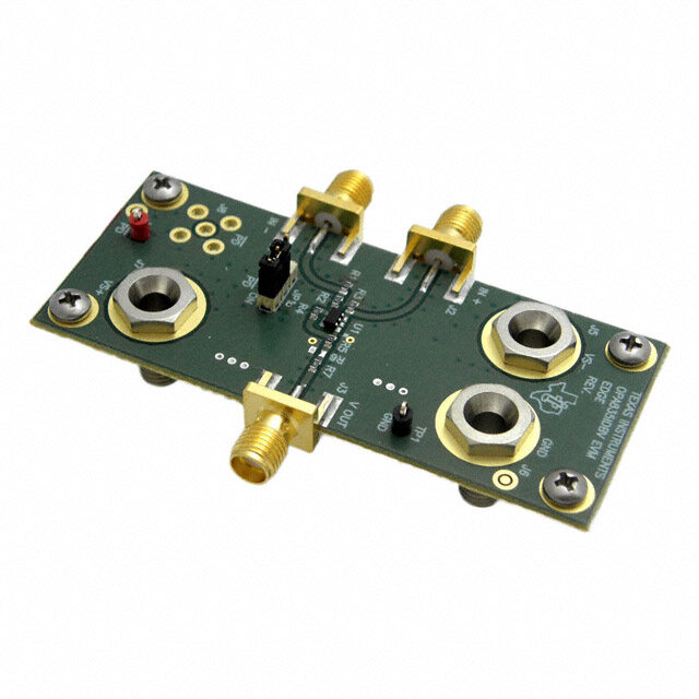
ICGOO电子元器件商城为您提供AD603-EVALZ由Analog设计生产,在icgoo商城现货销售,并且可以通过原厂、代理商等渠道进行代购。 AD603-EVALZ价格参考¥802.98-¥802.98。AnalogAD603-EVALZ封装/规格:评估板 - 运算放大器, AD603 X-AMP® Series 1 - Single Channels per IC Variable Gain Amplifier Evaluation Board。您可以下载AD603-EVALZ参考资料、Datasheet数据手册功能说明书,资料中有AD603-EVALZ 详细功能的应用电路图电压和使用方法及教程。
AD603-EVALZ 是由 Analog Devices Inc.(现为 Analog Devices, Inc.,简称 ADI)生产的一款用于评估 AD603 运算放大器的评估板。AD603 是一款高性能、宽带宽的可变增益放大器(VGA),广泛应用于需要高精度和高速信号处理的场合。

 应用场景:

1. 通信系统:
   AD603-EVALZ 适用于各种通信系统中的前端信号调理。它可以在射频(RF)和中频(IF)信号链中提供精确的增益控制,确保信号在传输过程中保持高质量。例如,在无线基站、卫星通信设备以及软件定义无线电(SDR)系统中,AD603 可以帮助实现动态范围扩展和噪声抑制。

2. 测试与测量设备:
   在精密测量仪器中,如示波器、频谱分析仪和网络分析仪,AD603 的高线性度和低失真特性使其成为理想的选择。通过 AD603-EVALZ,工程师可以轻松评估其在不同工作条件下的性能,确保最终产品能够满足严格的测量标准。

3. 音频处理:
   对于专业音频设备,如混音器、麦克风前置放大器和录音设备,AD603 提供了出色的增益调节能力,能够在不引入额外噪声的情况下放大微弱信号。这使得它非常适合用于高端音频应用,确保声音质量的纯净和稳定。

4. 医疗设备:
   在医疗电子领域,特别是超声成像、心电图(ECG)和脑电图(EEG)等设备中,AD603 的高精度和低噪声特性有助于提高信号采集的准确性。通过 AD603-EVALZ,研发人员可以优化电路设计,确保医疗设备的可靠性和安全性。

5. 工业自动化:
   在工业控制系统中,AD603 可用于传感器信号调理和反馈回路中,提供稳定的增益控制。这对于确保自动化系统的精确性和响应速度至关重要。例如,在机器人控制、过程监控和数据采集系统中,AD603 的高性能表现可以显著提升系统的整体性能。

总之,AD603-EVALZ 为工程师提供了一个便捷的平台,用于评估和验证 AD603 在各种应用场景中的性能。通过这个评估板,用户可以快速搭建原型,进行详细的性能测试,并优化设计方案,从而加速产品的开发周期。
| 参数 | 数值 |
| -3db带宽 | 90MHz |
| 产品目录 | 编程器,开发系统嵌入式解决方案 |
| 描述 | BOARD EVALUATION FOR AD603放大器 IC 开发工具 AD603 EVAL BRD |
| 产品分类 | |
| 品牌 | Analog Devices Inc |
| 产品手册 | |
| 产品图片 |
|
| rohs | 符合RoHS无铅 / 符合限制有害物质指令(RoHS)规范要求 |
| 产品系列 | 模拟与数字IC开发工具,放大器 IC 开发工具,Analog Devices AD603-EVALZX-AMP® |
| 数据手册 | |
| 产品型号 | AD603-EVALZ |
| 产品 | Evaluation Boards |
| 产品培训模块 | http://www.digikey.cn/PTM/IndividualPTM.page?site=cn&lang=zhs&ptm=30008 |
| 产品目录页面 | |
| 产品种类 | 放大器 IC 开发工具 |
| 使用的IC/零件 | AD603 |
| 其它名称 | AD603EVALZ |
| 压摆率 | 275 V/µs |
| 可用增益调整 | 31 dB |
| 商标 | Analog Devices |
| 封装 | Bulk |
| 工作温度 | -40°C ~ 85°C |
| 工作电源电压 | 5 V |
| 工作电源电流 | 12.5 mA |
| 工具用于评估 | AD603 |
| 工厂包装数量 | 1 |
| 所含物品 | 板 |
| 接口类型 | Parallel, Serial |
| 描述/功能 | Low noise, voltage-controlled amplifier |
| 放大器类型 | 可变增益 |
| 最大工作温度 | + 85 C |
| 最小工作温度 | - 40 C |
| 板类型 | 完全填充 |
| 标准包装 | 1 |
| 每IC通道数 | 1 - 单 |
| 用于 | AD603 |
| 电压-电源,单/双 (±) | 9.5 V ~ 12.6 V, ±4.75 V ~ 6.3 V |
| 电流-电源(主IC) | 12.5mA |
| 电流-输出/通道 | 50mA |
| 相关产品 | /product-detail/zh/AD603AQ/AD603AQ-ND/612067/product-detail/zh/AD603AR/AD603AR-ND/612071/product-detail/zh/AD603AR-REEL/AD603AR-REELTR-ND/617725/product-detail/zh/AD603AR-REEL7/AD603AR-REEL7TR-ND/617726/product-detail/zh/AD603ARZ/AD603ARZ-ND/617727/product-detail/zh/AD603ARZ-REEL/AD603ARZ-REELTR-ND/617728/product-detail/zh/AD603ARZ-REEL7/AD603ARZ-REEL7TR-ND/617729/product-detail/zh/AD603AR-REEL7/AD603AR-REEL7CT-ND/656125/product-detail/zh/AD603AR-REEL7/AD603AR-REEL7DKR-ND/741622 |
| 类型 | Variable Gain Amplifiers |
| 系列 | AD603 |
| 视频文件 | http://www.digikey.cn/classic/video.aspx?PlayerID=1364138032001&width=640&height=505&videoID=2219614204001http://www.digikey.cn/classic/video.aspx?PlayerID=1364138032001&width=640&height=505&videoID=2219593451001http://www.digikey.cn/classic/video.aspx?PlayerID=1364138032001&width=640&height=505&videoID=2219614205001 |
| 输出类型 | 单端 |



- 商务部:美国ITC正式对集成电路等产品启动337调查
- 曝三星4nm工艺存在良率问题 高通将骁龙8 Gen1或转产台积电
- 太阳诱电将投资9.5亿元在常州建新厂生产MLCC 预计2023年完工
- 英特尔发布欧洲新工厂建设计划 深化IDM 2.0 战略
- 台积电先进制程称霸业界 有大客户加持明年业绩稳了
- 达到5530亿美元!SIA预计今年全球半导体销售额将创下新高
- 英特尔拟将自动驾驶子公司Mobileye上市 估值或超500亿美元
- 三星加码芯片和SET,合并消费电子和移动部门,撤换高东真等 CEO
- 三星电子宣布重大人事变动 还合并消费电子和移动部门
- 海关总署:前11个月进口集成电路产品价值2.52万亿元 增长14.8%


PDF Datasheet 数据手册内容提取
Low Noise, 90 MHz Variable Gain Amplifier Data Sheet AD603 FEATURES The decibel gain is linear in dB, accurately calibrated, and stable over temperature and supply. The gain is controlled at a high Linear-in-dB gain control impedance (50 MΩ), low bias (200 nA) differential input; the Pin-programmable gain ranges scaling is 25 mV/dB, requiring a gain control voltage of only −11 dB to +31 dB with 90 MHz bandwidth 1 V to span the central 40 dB of the gain range. An overrange 9 dB to 51 dB with 9 MHz bandwidth and underrange of 1 dB is provided whatever the selected range. Any intermediate range, for example −1 dB to +41 dB The gain control response time is less than 1 μs for a 40 dB change. with 30 MHz bandwidth Bandwidth independent of variable gain The differential gain control interface allows the use of either 1.3 nV/√Hz input noise spectral density differential or single-ended positive or negative control voltages. ±0.5 dB typical gain accuracy Several of these amplifiers may be cascaded and their gain control gains offset to optimize the system SNR. APPLICATIONS The AD603 can drive a load impedance as low as 100 Ω with low distortion. For a 500 Ω load in shunt with 5 pF, the total RF/IF AGC amplifiers harmonic distortion for a ±1 V sinusoidal output at 10 MHz is Video gain controls typically −60 dBc. The peak specified output is ±2.5 V minimum A/D range extensions into a 500 Ω load. Signal measurements The AD603 uses a patented proprietary circuit topology—the X-AMP®. The X-AMP comprises a variable attenuator of 0 dB GENERAL DESCRIPTION to −42.14 dB followed by a fixed-gain amplifier. Because of the The AD603 is a low noise, voltage-controlled amplifier for use attenuator, the amplifier never has to cope with large inputs and in RF and IF AGC systems. It provides accurate, pin-selectable can use negative feedback to define its (fixed) gain and dynamic gains of −11 dB to +31 dB with a bandwidth of 90 MHz or +9 dB to performance. The attenuator has an input resistance of 100 Ω, 51+ dB with a bandwidth of 9 MHz. Any intermediate gain laser trimmed to ±3%, and comprises a 7-stage R-2R ladder range may be arranged using one external resistor. The input network, resulting in an attenuation between tap points of referred noise spectral density is only 1.3 nV/√Hz, and power 6.021 dB. A proprietary interpolation technique provides a consumption is 125 mW at the recommended ±5 V supplies. continuous gain control function that is linear in dB. The AD603 is specified for operation from −40°C to +85°C. FUNCTIONAL BLOCK DIAGRAM SCALING PRECISIONPASSIVE FIXED-GAIN REFERENCE INPUTATTENUATOR AMPLIFIER GPOS VOUT VG GNEG 6.44kΩ* GAIN- AD603 CONTROL FDBK INTERFACE 694Ω* 0dB –6.02dB –12.04dB –18.06dB –24.08dB –30.1dB –36.12dB –42.14dB VINP R R R R R R R 20Ω* 2R 2R 2R 2R 2R 2R R COMM *NOMINALVALUES. R-2R LADDER NETWORK 00539-001 Figure 1. Rev. K Information furnished by Analog Devices is believed to be accurate and reliable. However, no responsibility is assumed by Analog Devices for its use, nor for any infringements of patents or other One Technology Way, P.O. Box 9106, Norwood, MA 02062-9106, U.S.A. rights of third parties that may result from its use. Specifications subject to change without notice. No license is granted by implication or otherwise under any patent or patent rights of Analog Devices. Tel: 781.329.4700 www.analog.com Trademarks and registered trademarks are the property of their respective owners. Fax: 781.461.3113 ©1993–2012 Analog Devices, Inc. All rights reserved.
AD603 Data Sheet TABLE OF CONTENTS Features .............................................................................................. 1 The Gain Control Interface ....................................................... 13 Applications ....................................................................................... 1 Programming the Fixed-Gain Amplifier Using Pin General Description ......................................................................... 1 Strapping ...................................................................................... 13 Functional Block Diagram .............................................................. 1 Using the AD603 in Cascade ........................................................ 15 Revision History ............................................................................... 2 Sequential Mode (Optimal SNR) ............................................. 15 Specifications ..................................................................................... 3 Parallel Mode (Simplest Gain Control Interface) .................. 16 Absolute Maximum Ratings ............................................................ 4 Low Gain Ripple Mode (Minimum Gain Error) ................... 17 ESD Caution .................................................................................. 4 Applications Information .............................................................. 18 Pin Configurations and Function Descriptions ........................... 5 A Low Noise AGC Amplifier .................................................... 18 Typical Performance Characteristics ............................................. 6 Caution ........................................................................................ 19 Test Circuits ..................................................................................... 11 Evaluation Board ............................................................................ 20 Theory of Operation ...................................................................... 12 Outline Dimensions ....................................................................... 22 Noise Performance ..................................................................... 12 Ordering Guide .......................................................................... 23 REVISION HISTORY 4/12—Rev. J to Rev. K 3/05—Rev. F to Rev. G Changes to Table 1 ............................................................................ 3 Updated Format .................................................................. Universal Added Figure 10 and Figure 11; Renumbered Sequentially ....... 7 Change to Features ............................................................................ 1 Added Test Circuits Section .......................................................... 11 Changes to General Description ..................................................... 1 Moved Figure 29 and Figure 30 .................................................... 11 Change to Figure 1 ............................................................................ 1 Changes to Specifications ................................................................. 3 12/11—Rev. I to Rev. J New Figure 4 and Renumbering Subsequent Figures .................. 6 Changes to Figure 1 ......................................................................... 1 Change to Figure 10 .......................................................................... 7 Changes to Evaluation Board Section .......................................... 19 Change to Figure 23 .......................................................................... 9 Changes to Figure 48 Through Figure 50 .................................... 19 Change to Figure 29 ....................................................................... 12 Changes to Figure 51 Through Figure 54 .................................... 20 Updated Outline Dimensions ....................................................... 20 Added Figure 57 .............................................................................. 22 4/04—Rev. E to Rev. F Changes to Specifications ................................................................. 2 5/07—Rev. G to Rev. H Changes to Ordering Guide ............................................................. 3 Changes to Layout .......................................................................... 14 Changes to Layout .......................................................................... 15 8/03—Rev. D to Rev E Changes to Layout .......................................................................... 16 Updated Format .................................................................. Universal Inserted Evaluation Board Section, and Figure 48 to Changes to Specifications ................................................................. 2 Figure 51 .......................................................................................... 19 Changes to TPCs 2, 3, 4 .................................................................... 4 Inserted Figure 52 and Table 4 ...................................................... 20 Changes to Sequential Mode (Optimal S/N Ratio) section ......... 9 Changes to Ordering Guide .......................................................... 21 Change to Figure 8 ......................................................................... 10 Updated Outline Dimensions ....................................................... 14 Rev. K | Page 2 of 24
Data Sheet AD603 SPECIFICATIONS @ T = 25°C, V = ±5 V, –500 mV ≤ V ≤ +500 mV, GNEG = 0 V, –10 dB to +30 dB gain range, R = 500 Ω, and C = 5 pF, unless A S G L L otherwise noted. Table 1. Parameter Conditions Min Typ Max Unit INPUT CHARACTERISTICS Input Resistance Pin 3 to Pin 4 97 100 103 Ω Input Capacitance 2 pF Input Noise Spectral Density1 Input short-circuited 1.3 nV/√Hz Noise Figure f = 10 MHz, gain = maximum, R = 10 Ω 8.8 dB S 1 dB Compression Point f = 10 MHz, gain = maximum, R = 10 Ω −11 dBm S Peak Input Voltage ±1.4 ±2 V OUTPUT CHARACTERISTICS −3 dB Bandwidth V = 100 mV rms 90 MHz OUT Slew Rate R ≥ 500 Ω 275 V/µs L Peak Output2 R ≥ 500 Ω ±2.5 ±3.0 V L Output Impedance f ≤ 10 MHz 2 Ω Output Short-Circuit Current 50 mA Group Delay Change vs. Gain f = 3 MHz; full gain range ±2 ns Group Delay Change vs. Frequency V = 0 V; f = 1 MHz to 10 MHz ±2 ns G Differential Gain 0.2 % Differential Phase 0.2 Degree Total Harmonic Distortion f = 10 MHz, V = 1 V rms −60 dBc OUT Third-Order Intercept f = 40 MHz, gain = maximum, R = 50 Ω 15 dBm S ACCURACY Gain Accuracy, f = 100 kHz; Gain (dB) = (40 V + 10) dB −500 mV ≤ V ≤ +500 mV −1 ±0.5 +1 dB G G T to T −1.5 +1.5 dB MIN MAX Gain, f = 10.7 MHz V = -0.5 V −10.3 −9.0 −8.0 dB G V = 0.0 V +9.5 +10.5 +11.5 dB G V = 0.5 V +29.3 +30.3 +31.3 dB G Output Offset Voltage3 V = 0 V 20 mV G T to T 30 mV MIN MAX Output Offset Variation vs. V −500 mV ≤ V ≤ +500 mV 20 mV G G T to T 30 mV MIN MAX GAIN CONTROL INTERFACE Gain Scaling Factor 100 kHz 39.4 40 40.6 dB/V T to T 38 42 dB/V MIN MAX 10.7 MHz 38.7 39.3 39.9 dB/V GNEG, GPOS Voltage Range4 −1.2 +2.0 V Input Bias Current 50 100 250 nA Input Offset Current 10 nA Differential Input Resistance Pin 1 to Pin 2 50 MΩ Response Rate Full 40 dB gain change 80 dB/µs POWER SUPPLY Specified Operating Range ±4.75 ±6.3 V Quiescent Current 12.5 17 mA T to T 20 mA MIN MAX 1 Typical open or short-circuited input; noise is lower when system is set to maximum gain and input is short-circuited. This figure includes the effects of both voltage and current noise sources. 2 Using resistive loads of 500 Ω or greater or with the addition of a 1 kΩ pull-down resistor when driving lower loads. 3 The dc gain of the main amplifier in the AD603 is ×35.7; therefore, an input offset of 100 µV becomes a 3.57 mV output offset. 4 GNEG and GPOS, gain control, and voltage range are guaranteed to be within the range of −V + 4.2 V to +V − 3.4 V over the full temperature range of −40°C to +85°C. S S Rev. K | Page 3 of 24
AD603 Data Sheet ABSOLUTE MAXIMUM RATINGS Table 2. Parameter Rating Table 3. Thermal Characteristics Supply Voltage ±V ±7.5 V S Package Type θ θ Unit JA JC Internal Voltage VINP (Pin 3) ±2 V Continuous 8-Lead SOIC 155 33 °C/W ±V for 10 ms S 8-Lead CERDIP 140 15 °C/W GPOS, GNEG (Pin 1 and Pin2) ±V S Internal Power Dissipation 400 mW Operating Temperature Range ESD CAUTION AD603A −40°C to +85°C AD603S −55°C to +125°C Storage Temperature Range −65°C to +150°C Lead Temperature (Soldering, 60 sec) 300°C Stresses above those listed under Absolute Maximum Ratings may cause permanent damage to the device. This is a stress rating only; functional operation of the device at these or any other conditions above those indicated in the operational section of this specification is not implied. Exposure to absolute maximum rating conditions for extended periods may affect device reliability. Rev. K | Page 4 of 24
Data Sheet AD603 PIN CONFIGURATIONS AND FUNCTION DESCRIPTIONS GPOS 1 8 VPOS GPOS 1 8 VPOS GNEG 2 AD603 7 VOUT GNEG 2 AD603 7 VOUT COVMINMP 34 (NToOt Pto V SIEcWale) 65 VFDNBEKG 00539-002 COVMINMP 34 (NToOt Pto V SIEcWale) 65 VFDNBEKG 00539-003 Figure 2. 8-Lead SOIC Pin Configuration Figure 3. 8-Lead CERDIP Pin Configuration Table 4. Pin Function Descriptions Pin No. Mnemonic Description 1 GPOS Gain Control Input High (Positive Voltage Increases Gain). 2 GNEG Gain Control Input Low (Negative Voltage Increases Gain). 3 VINP Amplifier Input. 4 COMM Amplifier Ground. 5 FDBK Connection to Feedback Network. 6 VNEG Negative Supply Input. 7 VOUT Amplifier Output. 8 VPOS Positive Supply Input. Rev. K | Page 5 of 24
AD603 Data Sheet TYPICAL PERFORMANCE CHARACTERISTICS @ T = 25°C, V = ±5 V, –500 mV ≤ V ≤ +500 mV, GNEG = 0 V, –10 dB to +30 dB gain range, R = 500 Ω, and C = 5 pF, unless A S G L L otherwise noted. 40 4 225 3 180 30 2 135 1 90 20 0 GAIN 45 es) AIN (dB) 10.7MHz AIN (dB) –1 PHASE 0 E (Degre G 10 G –2 –45 AS H –3 –90 P 100kHz 0 –4 –135 –5 –180 –10–0.6 –0.4 –0.2 VG0 (V) 0.2 0.4 0.6 00539-004 –1600k 1M FREQUENCY 1(H0Mz) 100M –225 00539-007 Figure 4. Gain vs. V at 100 kHz and 10.7 MHz Figure 7. Frequency and Phase Response vs. Gain G (Gain = 10 dB, P = −30 dBm) IN 2.5 4 225 2.0 45MHz 3 180 2 135 1.5 1 90 ERROR (dB) 10..05 70MHz 10.7MHz AIN (dB) –10 PGHAAISNE 405 E (Degrees) AIN 0 G –2 –45 HAS G 455kHz –3 –90 P –0.5 70MHz –4 –135 –1.0 –5 –180 –1.5–0.5 –0.4 –0.3 –0.2 G–A0I.N1 VOL0TAGE0. 1(V) 0.2 0.3 0.4 0.5 00539-005 –1600k 1M FREQUENCY 1(H0Mz) 100M –225 00539-008 Figure 5. Gain Error vs. Gain Control Voltage at 455 kHz, Figure 8. Frequency and Phase Response vs. Gain 10.7 MHz, 45 MHz, 70 MHz (Gain = 30 dB, P = −30 dBm) IN 4 225 7.6 3 180 7.4 2 135 1 90 GAIN (dB) –––2130 PHGAASIEN 40––54950 PHASE (Degrees) GROUP DELAY (ns) 776...208 –4 –135 6.6 –5 –180 –1600k 1M FREQUENCY 1(H0Mz) 100M –225 00539-006 6.–40.6 –0.4 GA–I0N. 2CONTRO0L VOLTAG0.E2 (V) 0.4 0.6 00539-009 Figure 6. Frequency and Phase Response vs. Gain Figure 9. Group Delay vs. Gain Control Voltage (Gain = −10 dB, P = −30 dBm) IN Rev. K | Page 6 of 24
Data Sheet AD603 60 553 PIECE SAMPLE SIZE VOS AT 10dB GAIN VOS VS VGAIN 50 %) 10dB/DIV S ( E L 40 P M A S OF 30 E G A NT 20 E C R E P 10 0 2 4 6 OF8FSET1 0VOLT1A2GE (1m4V) 16 18 20 00539-057 00539-012 Figure 10. Histogram of VOS at 10 dB Gain and VOS vs. VGAIN Figure 13. Third-Order Intermodulation Distortion at 10.7 MHz (10× Probe Used to HP3585A Spectrum Analyzer, Gain = 0 dB, PIN = 0 dBm) 50 –1.0 553 PIECE SAMPLE SIZE –1.2 –1.4 %) 40 V) S ( E ( –1.6 E G PL GPOS TA –1.8 AM 30 GNEG OL –2.0 AGE OF S 20 OUTPUT V ––22..24 RCENT ATIVE ––22..68 PE 10 NEG –3.0 –3.2 0 85 PIN G90POS AN9D5 PIN GN10E0G BIAS1 0C5URREN11T0 (nA) 115 00539-058 –3.40 50 100LOAD2 R00ESISTA5N00CE (Ω)1000 2000 00539-013 Figure 14. Typical Output Voltage Swing vs. Load Resistance Figure 11. Histogram of GPOS and GNEG Bias Current (Negative Output Swing Limits First) 102 10dB/DIV Ω) 100 E ( C N A D 98 E P M T I U P 96 N I 94 00539-011 100k 1MFREQUENCY (Hz)10M 100M 00539-014 Figure 15. Input Impedance vs. Frequency (Gain = −10 dB) Figure 12. Third-Order Intermodulation Distortion at 455 kHz (10× Probe Used to HP3585A Spectrum Analyzer, Gain = 0 dB, PIN = 0 dBm) Rev. K | Page 7 of 24
AD603 Data Sheet 4.5V 102 INPUT GND 1V/DIV Ω) 100 E ( C N A D 98 500mV E P M T I U P 96 N I OUTPUT GND 500mV/DIV 94 100k 1MFREQUENCY (Hz)10M 100M 00539-015 –500m–V49ns 50ns 451ns 00539-018 Figure 19. Input Stage Overload Recovery Time Figure 16. Input Impedance vs. Frequency (Gain = 10 dB) (Input Is 500 ns Period, 50% Duty-Cycle Square Wave, Output Is Captured Using Tektronix 11402 Digitizing Oscilloscope) 102 3V Ω) 100 E ( INPUT GND C 100MV/DIV N A D 98 E P M 1V T I PU 96 OUTPUT GND N 1V/DIV I 94 100Fkigure 17. Input Im1MpFeRdEaQncUeE vN sC. YF r(eHqz)u10eMncy (Gain = 30 d1B0)0 M 00539-016 –2–V49ns 50ns 451ns 00539-019 Figure 20. Output Stage Overload Recovery Time (Input Is 500 ns Period, 50% Duty-Cycle Square Wave, Output Is Captured Using Tektronix 11402 Digitizing Oscilloscope) 3.5V 1V INPUT 100 500mV/DIV 90 GND 500mV OUTPUT 500mV/DIV GND 10 0% Figur1eV 18. Gain Control Channel R2e0s0pnosnse Time 00539-017 –1.5–V44ns 50ns 456ns 00539-020 Figure 21. Transient Response, G = 0 dB (Input Is 500 ns Period, 50% Duty-Cycle Square Wave, Output Is Captured Using Tektronix 11402 Digitizing Oscilloscope) Rev. K | Page 8 of 24
Data Sheet AD603 3.5V 21 TA = 25°C 10MHz RS = 50Ω 19 TEST SETUP FIGURE 23 17 INPUT GND 100mV/DIV B) 20MHz d 15 E ( R 500mV U 13 G O5U0T0PmUVT/ DGIVND SE FI 11 OI N 9 7 –1.5–V44ns 50ns 456ns 00539-021 530 31 32 33 34GAIN35 (dB)36 37 38 39 40 00539-025 Figure 22. Transient Response, G = 20 dB Figure 25. Noise Figure in 0 dB/40 dB Mode (Input Is 500 ns Period, 50% Duty-Cycle Square Wave, Output Is Captured Using Tektronix 11402 Digitizing Oscilloscope) 0 TA = 25°C TEST SETUP FIGURE 23 0 –5 –10 –20 m) dB –10 B) –30 EL ( RR (d –40 T LEV –15 PS –50 PU N I –60 –20 100k 1MFREQUENCY (Hz)10M 100M 00539-022 Fig–u2r5e1 026. 1 dB CompreIsNs3Pi0oUnT PFoRiEnQt,U −E1N0C dYB (/M+5H03z0) dB Mode, Gain 7=0 30 00539-026dB Figure 23. PSRR vs. Frequency (Worst Case Is Negative Supply PSRR, Shown Here) 20 23 TA = 25°C TA = 25°C TEST SETUP FIGURE 23 21 70MHz RTES S=T 5 S0VETUP FIGURE 23 18 30MHz 19 m) 16 FIGURE (dB) 111753 50MHz UT LEVEL (dB 14 40MHz NOISE 11 30MHz 10MHz OUTP 12 70MHz 9 10 7 520 21 22 23 24GAIN25 (dB)26 27 28 29 30 00539-024 Figu0–2re0 27. Third-Order InItNePrcUeTp Lt E–−1V10E0L d(dBB/+m3)0 dB Mode, Gain = 010 dB00539-027 Figure 24. Noise Figure in −10 dB/+30 dB Mode Rev. K | Page 9 of 24
AD603 Data Sheet 20 TA = 25°C RS = 50Ω 18 RRILN = = 1 5000ΩΩ 30MHz TEST SETUP FIGURE 23 m) 16 B L (d 40MHz E V 14 E L T U TP 12 U O 70MHz 10 8–40 INPUT LE–3V0EL (dBm) –20 00539-028 Figure 28. Third-Order Intercept −10 dB/+30 dB Mode, Gain = 30 dB Rev. K | Page 10 of 24
Data Sheet AD603 TEST CIRCUITS +5V 0.1µF HP3326A 8 DUAL- 3 CHANNEL SYNTHESIZER AD603 5 7 10× SHPEPC35T8R5UAM 100Ω 2 PROBE ANALYZER 4 1 511Ω 6 0.1µF –5VDDVCAT 8E5L00 00539-010 Figure 29. Third-Order Intermodulation Distortion Test Setup +5V 0.1µF HP3326A 8 DUAL- 3 CHANNEL SYNTHESIZER AD603 5 7 50Ω SHPEPC35T8R5UAM 100Ω 2 ANALYZER 4 1 6 0.1µF –5V DDVCAT 8E5L00 00539-023 Figure 30. Test Setup Used for: Noise Figure, Third-Order Intercept, and 1 dB Compression Point Measurements Rev. K | Page 11 of 24
AD603 Data Sheet THEORY OF OPERATION The AD603 comprises a fixed-gain amplifier, preceded by a The gain is at all times very exactly determined, and a linear-in- broadband passive attenuator of 0 dB to 42.14 dB, having a gain dB relationship is automatically guaranteed by the exponential control scaling factor of 40 dB per volt. The fixed gain is laser- nature of the attenuation in the ladder network (the X-AMP trimmed in two ranges, to either 31.07 dB (×35.8) or 50 dB principle). In practice, the gain deviates slightly from the ideal (×358), or it may be set to any range in between using one law, by about ±0.2 dB peak (see, for example, Figure 5). external resistor between Pin 5 and Pin 7. Somewhat higher NOISE PERFORMANCE gain can be obtained by connecting the resistor from Pin 5 to An important advantage of the X-AMP is its superior noise common, but the increase in output offset voltage limits the performance. The nominal resistance seen at inner tap points is maximum gain to about 60 dB. For any given range, the 41.7 Ω (one third of 125 Ω), which exhibits a Johnson noise bandwidth is independent of the voltage-controlled gain. This spectral density (NSD) of 0.83 nV/√Hz (that is, √4kTR) at 27°C, system provides an underrange and overrange of 1.07 dB in all which is a large fraction of the total input noise. The first stage cases; for example, the overall gain is −11.07 dB to +31.07 dB in of the amplifier contributes a further 1 nV/√Hz, for a total input the maximum bandwidth mode (Pin 5 and Pin 7 strapped). noise of 1.3 nV/√Hz. It is apparent that it is essential to use a This X-AMP structure has many advantages over former low resistance in the ladder network to achieve the very low methods of gain control based on nonlinear elements. Most specified noise level. The source impedance of the signal importantly, the fixed-gain amplifier can use negative feedback forms a voltage divider with the 100 Ω input resistance of the to increase its accuracy. Because large inputs are first attenuated, AD603. In some applications, the resulting attenuation may the amplifier input is always small. For example, to deliver a be unacceptable, requiring the use of an external buffer or ±1 V output in the −1 dB/+41 dB mode (that is, using a fixed preamplifier to match a high impedance source to the low amplifier gain of 41.07 dB), its input is only 8.84 mV; therefore, impedance AD603. the distortion can be very low. Equally important, the small- The noise at maximum gain (that is, at the 0 dB tap) depends on signal gain and phase response, and thus the pulse response, are whether the input is short-circuited or open-circuited. When essentially independent of gain. short-circuited, the minimum NSD of slightly over 1 nV/√Hz is Figure 31 is a simplified schematic. The input attenuator is a achieved. When open-circuited, the resistance of 100 Ω looking 7-section R-2R ladder network, using untrimmed resistors of into the first tap generates 1.29 nV/√Hz, so the noise increases nominally R = 62.5 Ω, which results in a characteristic resistance of to 1.63 nV/√Hz. (This last calculation would be important if the 125 Ω ± 20%. A shunt resistor is included at the input and laser AD603 were preceded by, for example, a 900 Ω resistor to allow trimmed to establish a more exact input resistance of 100 Ω ± 3%, operation from inputs up to 10 V rms.) As the selected tap which ensures accurate operation (gain and HP corner frequency) moves away from the input, the dependence of the noise on when used in conjunction with external resistors or capacitors. source impedance quickly diminishes. The nominal maximum signal at input VINP is 1 V rms Apart from the small variations just discussed, the signal-to- (±1.4 V peak) when using the recommended ±5 V supplies, noise (SNR) at the output is essentially independent of the although operation to ±2 V peak is permissible with some attenuator setting. For example, on the −11 dB/+31 dB range, increase in HF distortion and feedthrough. Pin 4 (COMM) the fixed gain of ×35.8 raises the output NSD to 46.5 nV/√Hz. must be connected directly to the input ground; significant Therefore, for the maximum undistorted output of 1 V rms and impedance in this connection reduces the gain accuracy. a 1 MHz bandwidth, the output SNR would be 86.6 dB, that is, The signal applied at the input of the ladder network is attenuated 20 log(1 V/46.5 µV). by 6.02 dB by each section; therefore, the attenuation to each of the taps is progressively 0 dB, 6.02 dB, 12.04 dB, 18.06 dB, 24.08 dB, 30.1 dB, 36.12 dB, and 42.14 dB. A unique circuit technique is employed to interpolate between these tap points, indicated by the slider in Figure 31, thus providing continuous attenuation from 0 dB to 42.14 dB. It helps in understanding the AD603 to think in terms of a mechanical means for moving this slider from left to right; in fact, its position is controlled by the voltage between Pin 1 and Pin 2. The details of the gain control interface are in the The Gain Control Interface section. Rev. K | Page 12 of 24
Data Sheet AD603 VPOS 8 SCALING PRECISIONPASSIVE FIXED-GAIN REFERENCE INPUTATTENUATOR AMPLIFIER VNEG 6 GPOS 1 7 VOUT VG GNEG 2 6.44kΩ* GAIN- AD603 CONTROL INTERFACE 5 FDBK 694Ω* 0dB –6.02dB –12.04dB –18.06dB –24.08dB –30.1dB –36.12dB –42.14dB VINP 3 R R R R R R R 20Ω* 2R 2R 2R 2R 2R 2R R COMM 4 R-2R LADDER NETWORK *NOMINALVALUES. 00539-029 Figure 31. Simplified Block Diagram THE GAIN CONTROL INTERFACE For example, if the gain is to be controlled by a DAC providing a positive-only, ground-referenced output, the gain control low The attenuation is controlled through a differential, high (GNEG) pin should be biased to a fixed offset of 500 mV to set impedance (50 MΩ) input, with a scaling factor that is laser- the gain to −10 dB when gain control high (GPOS) is at zero, trimmed to 40 dB per volt, that is, 25 mV/dB. An internal band and to 30 dB when at 1.00 V. gap reference ensures stability of the scaling with respect to supply and temperature variations. It is a simple matter to include a voltage divider to achieve other scaling factors. When using an 8-bit DAC having an FS output When the differential input voltage V = 0 V, the attenuator G of 2.55 V (10 mV/bit), a divider ratio of 2 (generating 5 mV/bit) slider is centered, providing an attenuation of 21.07 dB. For the results in a gain-setting resolution of 0.2 dB/bit. The use of such maximum bandwidth range, this results in an overall gain of offsets is valuable when two AD603s are cascaded, when 10 dB (= −21.07 dB + 31.07 dB). When the control input is various options exist for optimizing the signal-to-noise profile, −500 mV, the gain is lowered by +20 dB (= 0.500 V × 40 dB/V) as is shown in the Sequential Mode (Optimal SNR) section, to −10 dB; when set to +500 mV, the gain is increased by +20 dB to +30 dB. When this interface is overdriven in either PROGRAMMING THE FIXED-GAIN AMPLIFIER direction, the gain approaches either −11.07 dB (= − 42.14 dB + USING PIN STRAPPING +31.07 dB) or 31.07 dB (= 0 + 31.07 dB), respectively. The only Access to the feedback network is provided at Pin 5 (FDBK). constraint on the gain control voltage is that it be kept within The user may program the gain of the output amplifier of the the common-mode range (−1.2 V to +2.0 V assuming +5 V AD603 using this pin, as shown in Figure 32, Figure 33, and supplies) of the gain control interface. Figure 34. There are three modes: in the default mode, FDBK The basic gain of the AD603 can therefore be calculated by is unconnected, providing the range +9 dB/+51 dB; when V OUT and FDBK are shorted, the gain is lowered to −11 dB/+31 dB; Gain (dB) = 40 V +10 (1) G and, when an external resistor is placed between V and OUT where V is in volts. When Pin 5 and Pin 7 are strapped (see the G FDBK, any intermediate gain can be achieved, for example, Programming the Fixed-Gain Amplifier Using Pin Strapping −1 dB/+41 dB. Figure 35 shows the nominal maximum gain vs. section), the gain becomes external resistor for this mode. Gain (dB) = 40 V + 20 for 0 to +40 dB G VC1 1 GPOS VPOS 8 VPOS and AD603 Gain (dB) = 40 V + 30 for +10 to +50 dB (2) VC2 2 GNEG VOUT 7 VOUT G The high impedance gain control input ensures minimal VIN 3 VINP VNEG 6 VNEG loading when driving many amplifiers in multiple channel oflre xciabsicliatdye idn acphpoloicsaintigo nths.e Tahppe rdoipffreiraeten tsiiagln caalp laebviellist ya npdro vides 4 COMM FDBK 5 00539-030 Figure 32. −10 dB to +30 dB; 90 MHz Bandwidth polarities for various control schemes. Rev. K | Page 13 of 24
AD603 Data Sheet Optionally, when a resistor is placed from FDBK to COMM, VC1 1 GPOS VPOS 8 VPOS higher gains can be achieved. This fourth mode is of limited AD603 VC2 2 GNEG VOUT 7 VOUT value because of the low bandwidth and the elevated output offsets; it is thus not included in Figure 32, Figure 33, or VIN 3 VINP VNEG 6 VNEG Figure 34. 2.15kΩ The gain of this amplifier in the first two modes is set by the 4 COMM FDBK 5 5.6pF 00539-031 rreastiiost oorf so ins- vcehriyp alacsceurr-attreim, tmhee adb rseosliustteo rvsa. lWueh oilfe t htheese r aretisois otof rtsh ese Figure 33. 0 dB to 40 dB; 30 MHz Bandwidth can vary by as much as ±20%. Therefore, when an external resistor is connected in parallel with the nominal 6.44 kΩ ± 20% VC1 1 GPOS VPOS 8 VPOS internal resistor, the overall gain accuracy is somewhat poorer. AD603 The worst-case error occurs at about 2 kΩ (see Figure 36). VC2 2 GNEG VOUT 7 VOUT 1.2 VIN 3 VINP VNEG 6 VNEG 1.0 –1:VdB (OUT) – (–1):VdB (OREF) 0.8 4 COMM FDBK 5 18pF 00539-032 B) 00..64 Figure 34. 10 dB to 50 dB; 9 MHz to Set Gain R (d 0.2 O 52 R R 0 E 50 –1:VdB (OUT) N AI –0.2 48 G –0.4 46 –0.6 44 –0.8 B) 42 VdB (OUT) VdB (OUT) – VdB (OREF) GAIN (d 40 –2:VdB (OUT) –1.010 100 1kREXT (Ω)10k 100k 1M 00539-034 38 Figure 36. Worst-Case Gain Error, Assuming Internal Resistors Have a 36 Maximum Tolerance of −20% (Top Curve) or = 20% (Bottom Curve) 34 While the gain bandwidth product of the fixed-gain amplifier is 32 about 4 GHz, the actual bandwidth is not exactly related to the 3010 100 1kREXT (Ω)10k 100k 1M 00539-033 mthaex aicm ruemsp ognaisne. mTahgisn iistu bdeec aouns eth teh emrea xisim a uslmig hbta nendhwaindcthin rga nofg e, Figure 35. Gain vs. R , Showing Worst-Case Limits Assuming Internal due to higher order poles in the open-loop gain function; this EXT Resistors Have a Maximum Tolerance of 20% mild peaking is not present on the higher gain ranges. Figure 32, Figure 33, and Figure 34 show how an optional capacitor may be added to extend the frequency response in high gain modes. Rev. K | Page 14 of 24
Data Sheet AD603 USING THE AD603 IN CASCADE Two or more AD603s can be connected in series to achieve Figure 37 shows the SNR over a gain range of −22 dB to +62 dB, higher gain. Invariably, ac coupling must be used to prevent the assuming an output of 1 V rms and a 1 MHz bandwidth. Figure 38, dc offset voltage at the output of each amplifier from overloading Figure 39, and Figure 40 show the general connections to the following amplifier at maximum gain. The required high- accomplish this. Here, both the positive gain control inputs pass coupling network is usually just a capacitor, chosen to set (GPOS) are driven in parallel by a positive-only, ground-referenced the desired corner frequency in conjunction with the well- source with a range of 0 V to 2 V, while the negative gain defined 100 Ω input resistance of the following amplifier. control inputs (GNEG) are biased by stable voltages to provide the needed gain offsets. These voltages may be provided by For two AD603s, the total gain control range becomes 84 dB resistive dividers operating from a common voltage reference. (2 × 42.14 dB); the overall −3 dB bandwidth of cascaded stages is somewhat reduced. Depending on the pin strapping, the gain 90 and bandwidth for two cascaded amplifiers can range from 85 −22 dB to +62 dB (with a bandwidth of about 70 MHz) to +22 dB to +102 dB (with a bandwidth of about 6 MHz). 80 There are several ways of connecting the gain control inputs 75 in cascaded operation. The choice depends on whether it is B) d 70 important to achieve the highest possible instantaneous signal- R ( N to-noise ratio (ISNR), or, alternatively, to minimize the ripple S 65 in the gain error. The following examples feature the AD603 60 programmed for maximum bandwidth; the explanations apply to other gain/bandwidth combinations with appropriate 55 changes to the arrangements for setting the maximum gain. SEQUENTIAL MODE (OPTIMAL SNR) 50–0.2 0.2 0.6 VC1 .(0V) 1.4 1.8 2.2 00539-035 In the sequential mode of operation, the ISNR is maintained at Figure 37. SNR vs. Control Voltage, Sequential Control (1 MHz Bandwidth) its highest level for as much of the gain control range as possible. A1 A2 –40.00dB –51.07dB INPUT –42.14dB 31.07dB –8.93dB –42.14dB 31.07dB OUTPUT 0dB GPOS GNEG GPOS GNEG –20dB VC = 0V VG1 VO1 = 0.473V VG2 VO2 = 1.526V 00539-036 Figure 38. AD603 Gain Control Input Calculations for Sequential Control Operation VC = 0 V 0dB –11.07dB INPUT 0dB 31.07dB 31.07dB –42.14dB 31.07dB OUTPUT 0dB GPOS GNEG GPOS GNEG 20dB VC = 1.0V VG1 VO1 = 0.473V VG2 VO2 = 1.526V 00539-037 Figure 39. AD603 Gain Control Calculations for Sequential Control Operation VC = 1.0 V 0dB –28.93dB INPUT 0dB 31.07dB 31.07dB –2.14dB 31.07dB OUTPUT 0dB GPOS GNEG GPOS GNEG 60dB VC = 2.0V VG1 VO1 = 0.473V VG2 VO2 = 1.526V 00539-038 Figure 40. AD603 Gain Control Input Calculations for Sequential Operation VC = 2.0 V Rev. K | Page 15 of 24
AD603 Data Sheet The gains are offset (Figure 41) such that the gain of A2 is Figure 43 is a plot of the SNR of the cascaded amplifiers vs. the increased only after the gain of A1 has reached its maximum control voltage. Figure 44 is a plot of the gain error of the value. Note that for a differential input of –600 mV or less, the cascaded stages vs. the control voltages. gain of a single amplifier (A1 or A2) is at its minimum value of 70 −11.07 dB; for a differential input of 600 mV or more, the gain 60 is at its maximum value of 31.07 dB. Control inputs beyond COMBINED 50 these limits do not affect the gain and can be tolerated without damage or foldover in the response. This is an important aspect B) 40 A1 of the gain control response of the AD603. (See the Specifications N (d 30 section for more details on the allowable voltage range.) The GAI 20 L gain is now L A 10 R E Gain (dB) = 40 VG + GO (3) OV 0 A2 where: –10 VG is the applied control voltage. –20 G is determined by the gain range chosen. InO the explanatory notes that follow, it is assumed that –30–0.2 0.2 0.6 VC1 .(0V) 1.4 1.8 2.0 00539-040 the maximum bandwidth connections are used, for which Figure 42. Plot of Separate and Overall Gains in Sequential Control G is −20 dB. O 90 +31.07dB 80 +31.07dB +28.96dB 70 +10dB A1 * A2 –8.93dB –11.07dB * 60 –11.07dB B) d 50 0.473 1.526 R ( N S 40 GAIN 0 0.5 1.0 1.50 2.0 VC (V) (dB) –22.14 –20 0 20 40 60 62.14 *GAIN OFFSET OF 1.07dB, OR 26.75mV. 00539-039 3200 Figure 41. Explanation of Offset Calibration for Sequential Control WVGi1t hre rfeefresr teon cthe et od iFfifgeruernet 3ia8l, gFaiignu creo n3t9r,o aln indp Fuigt utor eA 410, ,a nnodt eV tGh2a t 10–0.2 0.2 0.6 VC1 .(0V) 1.4 1.8 2.0 00539-041 refers to the differential gain control input to A2. When V is Figure 43. SNR for Cascaded Stages—Sequential Control G 0 V, VG1 = −473 mV and thus the gain of A1 is −8.93 dB (recall 2.0 that the gain of each individual amplifier in the maximum 1.5 bandwidth mode is –10 dB for V = −500 mV and 10 dB for V G G = 0 V); meanwhile, V = −1.908 V so the gain of A2 is pinned 1.0 G2 at −11.07 dB. The overall gain is therefore –20 dB (see Figure 38). B) 0.5 d When VG = 1.00 V, VG1 = 1.00 V − 0.473 V = 0.526 V, which sets OR ( 0 the gain of A1 to nearly its maximum value of +31.07 dB, while R R E VG2 = 1.00 V − 1.526 V = 0.526 V, which sets the gain of A2 to AIN –0.5 nearly its minimum value of −11.07 dB. Close analysis shows G –1.0 that the degree to which neither AD603 is completely pushed to its maximum nor minimum gain exactly cancels in the overall –1.5 gain, which is now 20 dB (see Figure 39). When VG = 2.0 V, the gain of A1 is pinned at 31.07 dB and that –2.0–0.2 0 0.2 0.4 0.6 0.8VC1 .(0V)1.2 1.4 1.6 1.8 2.0 2.2 00539-042 of A2 is near its maximum value of 28.93 dB, resulting in an Figure 44. Gain Error for Cascaded Stages–Sequential Control overall gain of 60 dB (see Figure 40). This mode of operation is PARALLEL MODE (SIMPLEST GAIN CONTROL further clarified in Figure 42, which is a plot of the separate gains of A1 and A2 and the overall gain vs. the control voltage. INTERFACE) In this mode, the gain control of voltage is applied to both inputs in parallel: the GPOS pins of both A1 and A2 are Rev. K | Page 16 of 24
Data Sheet AD603 connected to the control voltage and the GNEW inputs are LOW GAIN RIPPLE MODE (MINIMUM GAIN ERROR) grounded. The gain scaling is then doubled to 80 dB/V, As can be seen in Figure 44 and Figure 45, the error in the gain requiring only a 1.00 V change for an 80 dB change of gain is periodic, that is, it shows a small ripple. (Note that there is Gain = (dB) = 80 V + G (4) also a variation in the output offset voltage, which is due to the G O gain interpolation, but this is not exact in amplitude.) By where, as before, G depends on the range selected; for example, O offsetting the gains of A1 and A2 by half the period of the ripple, in the maximum bandwidth mode, G is 20 dB. Alternatively, O that is, by 3 dB, the residual gain errors of the two amplifiers the GNEG pins may be connected to an offset voltage of can be made to cancel. Figure 47 shows much lower gain ripple 0.500 V, in which case G is −20 dB. O when configured in this manner. Figure 48 plots the ISNR as a The amplitude of the gain ripple in this case is also doubled, as function of gain; it is very similar to that in the parallel mode. shown in Figure 45, while the ISNR at the output of A2 now 3.0 decreases linearly as the gain increases, as shown in Figure 46. 2.5 2.0 2.0 1.5 1.5 1.0 1.0 R (dB) 0.5 B) 0.5 RO 0 RROR (d 0 GAIN ER ––01..50 E AIN –0.5 –1.5 G –2.0 –1.0 –2.5 ––12..50–0.2 0 0.2 0.4 0.6 0.8VC1 .(0V)1.2 1.4 1.6 1.8 2.0 2.2 00539-043 –3.F0–0ig.1ure0 47. 0G.1ain0 E.2rro0r .f3or C0.a4sVcCa0 .d(5Ve)d0 S.6tag0e.7s—0L.8ow0 R.9ipp1le.0 Mo1.d1e 00539-045 90 Figure 45. Gain Error for Cascaded Stages—Parallel Control 90 85 85 80 80 75 B) 75 R (d 70 R (dB) 70 ISN 65 N IS 65 60 60 55 5550–0.2 0 0.2 0.4VC (V)0.6 0.8 1.0 1.2 00539-044 50–0.2Figure0 48. ISN0R.2 vs. Con0.t4rVoCl V(Vo)l0ta.6ge—L0o.8w Ripp1le.0 Mode1 .2 00539-046 Figure 46. ISNR for Cascaded Stages—Parallel Control Rev. K | Page 17 of 24
AD603 Data Sheet APPLICATIONS INFORMATION A LOW NOISE AGC AMPLIFIER The circuit operates as follows: Figure 49 shows the ease with which the AD603 can be A1 and A2 are cascaded. connected as an AGC amplifier. The circuit illustrates many of Capacitor C1 and the 100 Ω of resistance at the input of A1 the points previously discussed: it uses few parts, has linear-in- form a time constant of 10 μs. dB gain, operates from a single supply, uses two cascaded amplifiers in sequential gain mode for maximum SNR, and an external C2 blocks the small dc offset voltage at the output of A1 resistor programs each gain of the amplifier. It also uses a (which might otherwise saturate A2 at its maximum gain) simple temperature-compensated detector. and introduces a high-pass corner at about 16 kHz, eliminating low frequency noise. The circuit operates from a single 10 V supply. Resistors R1, R2, R3, and R4 bias the common pins of A1 and A2 at 5 V. The A half-wave detector is used, based on Q1 and R8. The current common pin is a low impedance point and must have a low into capacitor, CAV, is the difference between the collector impedance path to ground, provided here by the 100 μF tantalum current of Q2 (biased to be 300 μA at 300 K, 27°C) and the capacitors and the 0.1 μF ceramic capacitors. collector current of Q1, which increases with the amplitude of the output signal. The cascaded amplifiers operate in sequential gain. Here, the offset voltage between Pin 2 (GNEG) of A1 and A2 is 1.05 V The automatic gain control voltage, VAGC, is the time integral (42.14 dB × 25 mV/dB), provided by a voltage divider consisting of of this error current. For VAGC (and thus the gain) to remain Resistors R5, R6, and R7. Using standard values, the offset is not insensitive to short-term amplitude fluctuations in the output exact, but it is not critical for this application. signal, the rectified current in Q1 must, on average, exactly balance the current in Q2. If the output of A2 is too small to The gain of both A1 and A2 is programmed by Resistors R13 do this, V increases, causing the gain to increase until Q1 and R14, respectively, to be about 42 dB; therefore, the maximum AGC conducts sufficiently. gain of the circuit is twice that, or 84 dB. The gain control range can be shifted up by as much as 20 dB by appropriate choices of Consider the case where R8 is zero and the output voltage VOUT R13 and R14. is a square wave at, for example, 455 kHz, which is well above the corner frequency of the control loop. 10V TAHGISC CTAIMPEA CCIOTONRST SAENTTS 1.54RkΩ9 R1.1204kΩ C0.111µF C7 Q2 0.1µF 10V VAGC 2N3906 C8 R11 C1 2.R419k3Ω 0.1µF 10V CAV 3.83kΩ 0.1µF 8 R14 0.1µF Q1 5V J1 10R0TΩ1 10V 3ADA61063 25 7 0.C12µF 3 8A26 5 2.49kΩ 2N38900R64Ω8 R4.1929kΩ C0.91µF R1 4 10V AD603 7 J2 2.49kΩ 1 2 C10 R3 4 0.1µF C32 + C4 R2 2.49kΩ 1 100µF 0.1µF 2.49kΩ C52 + C6 R4 100µF 0.1µF 2.49kΩ AGC LINE R5 1V OFFSET FOR R7 5.49kΩ SEQUENTIAL GAIN 3.48kΩ 10V 5.5V R6 6.5V 1.05kΩ 12RCT3 PARNODV CID5EASR AE 5T0AΩN TINAPLUUTM .IMPEDANCE. 00539-047 Figure 49. A Low Noise AGC Amplifier Rev. K | Page 18 of 24
Data Sheet AD603 During the time V is negative with respect to the base This resistor also serves to lower the peak current in Q1 when OUT voltage of Q1, Q1 conducts; when V is positive, it is cut off. more typical signals (usually sinusoidal) are involved, and the OUT Because the average collector current of Q1 is forced to be 1.8 kHz LP filter it forms with C helps to minimize distortion AV 300 µA, and the square wave has a duty cycle of 1:1, Q1’s due to ripple in V . Note that the output amplitude under sine AGC collector current when conducting must be 600 µA. With R8 wave conditions is higher than for a square wave because the omitted, the peak amplitude of V is forced to be just the V average value of the current for an ideal rectifier is 0.637 times OUT BE of Q1 at 600 µA, typically about 700 mV, or 2 V peak-to-peak. as large, causing the output amplitude to be 1.88 (= 1.2/0.637) V, BE This voltage, the amplitude at which the output stabilizes, has a or 1.33 V rms. In practice, the somewhat nonideal rectifier strong negative temperature coefficient (TC), typically −1.7 mV/°C. results in the sine-wave output being regulated to about Although this may not be troublesome in some applications, the 1.4 V rms, or 3.6 V p-p. correct value of R8 renders the output stable with temperature. The bandwidth of the circuit exceeds 40 MHz. At 10.7 MHz, the To understand this, note that the current in Q2 is made to be AGC threshold is 100 µV (−67 dBm) and its maximum gain is proportional to absolute temperature (PTAT). For the moment, 83 dB (20 log 1.4 V/100 µV). The circuit holds its output at continue to assume that the signal is a square wave. 1.4 V rms for inputs as low as −67 dBm to +15 dBm (82 dB), where the input signal exceeds the maximum input rating of the When Q1 is conducting, V is now the sum of V and a OUT BE AD603. For a 30 dBm input at 10.7 MHz, the second harmonic voltage that is PTAT and that can be chosen to have an equal is 34 dB down from the fundamental, and the third harmonic is but opposite TC to that of the V . This is actually nothing more BE 35 dB down from the fundamental. than an application of the band gap voltage reference principle. When R8 is chosen such that the sum of the voltage across it CAUTION and the V of Q1 is close to the band gap voltage of about 1.2 V, BE Careful component selection, circuit layout, power supply V is stable over a wide range of temperatures, provided, of OUT decoupling, and shielding are needed to minimize the susceptibility course, that Q1 and Q2 share the same thermal environment. of the AD603 to interference from signals such as those from Because the average emitter current is 600 µA during each half radio and TV stations. In bench evaluation, it is recommended cycle of the square wave, a resistor of 833 Ω adds a PTAT to place all of the components into a shielded box and use voltage of 500 mV at 300 K, increasing by 1.66 mV/°C. In feedthrough decoupling networks for the supply voltage. Circuit practice, the optimum value depends on the type of transistor layout and construction are also critical because stray capacitances used and, to a lesser extent, on the waveform for which the and lead inductances can form resonant circuits and are a temperature stability is to be optimized; for the inexpensive potential source of circuit peaking, oscillation, or both. 2N3904/2N3906 pair and sine wave signals, the recommended value is 806 Ω. Rev. K | Page 19 of 24
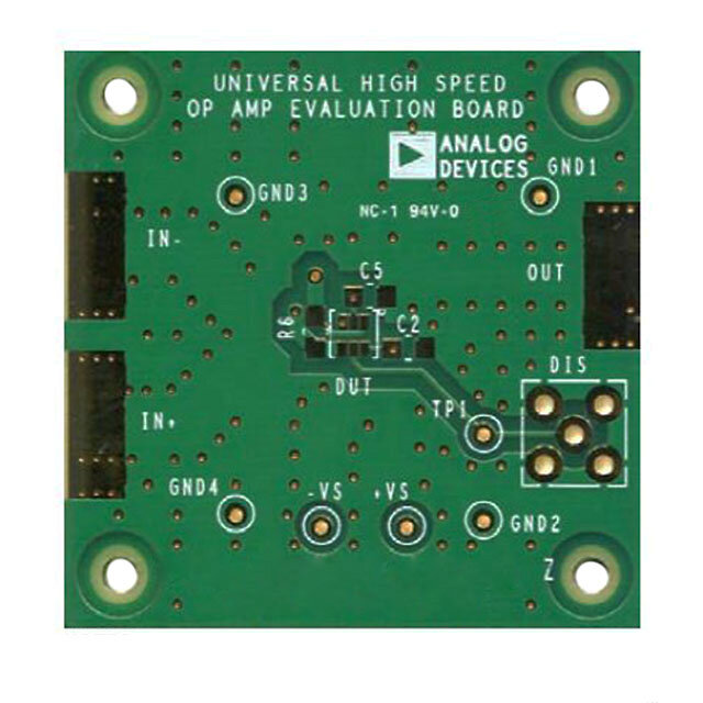
AD603 Data Sheet EVALUATION BOARD The evaluation board of the AD603 enables simple bench-top The output is also ac-coupled and includes a 453 Ω series resistor. experimenting to be performed with easy control of the Set the AD603 gain by connecting a voltage source between the AD603. Built-in flexibility allows convenient configuration to GNEG and GPOS test loops. The two slide switches SGPOS and accommodate most operating configurations. Figure 50 is a SGNEG provide three connections for GPOS and the GNEG. photograph of the AD603 evaluation board. Either pin can be ground referenced, or biased with a user selected voltage established by R1 and R5 to R7. A signal generator can be connected to the GPOS or GNEG test loops, or the GNEG can be driven to either polarity within the common-mode limits of −1.2 V to +2.0 V; to invert the gain slope, simply reverse the polarity of the voltage source connected to GPOS and GNEG. For bias current measurements, the third switch option disconnects the bias voltage source and permits connection of a microammeter between the GPOS and GNEG pins to ground. The AD603 includes built-in gain resistors selectable at the FDBK pin. The board is shipped with the gain at minimum, with a 0 Ω resistor installed in R3. For maximum gain, simply remove R3. Because of the architecture of the AD603, the 00539-049 bInatnedrmwieddtiha tdee gcariena sveasl ubeys 1 m0,a byu bte t hseel egcatiend r abny gien srteamllianing sa a rte 4si0s tdoBr . Figure 50. AD603 Evaluation Board between the VOUT and FDBK pins. Any dual-polarity power supply capable of providing 20 mA is Figure 52, Figure 53, and Figure 56 show the component and all that is required, in addition to whatever test equipment the circuit side copper patterns and silkscreen. user wishes to perform the intended tests. Referring to the schematic in Figure 51, the input to the VGA is single-ended, ac-coupled, and terminated in 50 Ω to accommodate most commonly available signal generators. VPOS GND VNEG G1 G2 G3 G4 G5 G6 C7 C8 10µF 10µF 25V 25V + + VPOS VNEG VPOS GPOS VPOS GPOSS C1 R7 SGPOS 0.1µF R1VNEG C0.21µF VO 00539-051 VPOS GNEGS GNEG AD603 0.C16µF 45R34Ω VOUT Figure 52. Component Side Copper C4 1 8 R6 SGNEG0.1µF GPOS VPOS W1 2 7 GNEG VOUT R5 0.C15µF 3 VINP VNEG 6 R0Ω3 VNEG VNEG 4 COMM FDBK 5 C3 0.1µF C9 VIN R2 W2 100Ω VPOS R8 SCOM RV9NEG 00539-050 Figure 51. Schematic of the AD603 Evaluation Board Rev. K | Page 20 of 24
Data Sheet AD603 00539-052 00539-054 Figure 53. Secondary Side Copper Figure 55. Inner Layer Power Plane 00539-053 00539-055 Figure 54. Inner Layer Ground Plane Figure 56. Component Side Silk Screen Rev. K | Page 21 of 24
AD603 Data Sheet OUTLINE DIMENSIONS 0.005 (0.13) 0.055 (1.40) MIN MAX 8 5 0.310 (7.87) 0.220 (5.59) 1 4 0.100 (2.54) BSC 0.405 (10.29) MAX 0.320 (8.13) 0.290 (7.37) 0.200 (5.08) 0.060 (1.52) MAX 0.015 (0.38) 0.200 (5.08) 0.150 (3.81) MIN 0.125 (3.18) 0.015 (0.38) 00..002134 ((00..5386)) 0.070 (1.78) SPELAANTIENG 1 05°° 0.008 (0.20) 0.030 (0.76) CONTROLLING DIMENSIONS ARE IN INCHES; MILLIMETER DIMENSIONS (IN PARENTHESES) ARE ROUNDED-OFF INCH EQUIVALENTS FOR REFERENCE ONLY AND ARE NOT APPROPRIATE FOR USE IN DESIGN. Figure 57. 8-Lead Ceramic Dual In-Line Package [CERDIP] (Q-8) Dimensions shown in inches and (millimeters) 5.00(0.1968) 4.80(0.1890) 8 5 4.00(0.1574) 6.20(0.2441) 3.80(0.1497) 1 4 5.80(0.2284) 1.27(0.0500) 0.50(0.0196) BSC 1.75(0.0688) 0.25(0.0099) 45° 0.25(0.0098) 1.35(0.0532) 8° 0.10(0.0040) 0° COPLANARITY 0.51(0.0201) 0.10 SEATING 0.31(0.0122) 0.25(0.0098) 10..2470((00..00510507)) PLANE 0.17(0.0067) COMPLIANTTOJEDECSTANDARDSMS-012-AA RC(INEOFNPEATRRREOENNLCLTEIHNEOGSNDELISYM)AEANNRDSEIAORRNOESUNANORDETEDAIN-POMPFRIFLOLMPIMIRLELIATIMTEEERTFSEO;RIRNECUQHSUEDIVIINMAELDENENSSTIIOGSNNFS.OR 012407-A Figure 58. 8-Lead Standard Small Outline Package [SOIC_N] Narrow Body (R-8) Dimensions shown in millimeters and (inches) Rev. K | Page 22 of 24
Data Sheet AD603 0.07 0.088 A (CTIROCPUI TV SIIEDEW) 12-07-2011- Figure 59. 9-Pad Bare Die [CHIP] (C-9-1) Dimensions Shown in Inches ORDERING GUIDE Model1, 2 Temperature Range Package Description Package Option AD603AR −40°C to +85°C 8-Lead SOIC_N R-8 AD603AR-REEL −40°C to +85°C 8-Lead SOIC_N, 13" Tape and Reel R-8 AD603AR-REEL7 −40°C to +85°C 8-Lead SOIC_N, 7" Tape and Reel R-8 AD603ARZ −40°C to +85°C 8-Lead SOIC_N R-8 AD603ARZ-REEL −40°C to +85°C 8-Lead SOIC_N, 13" Tape and Reel R-8 AD603ARZ-REEL7 −40°C to +85°C 8-Lead SOIC_N, 7" Tape and Reel R-8 AD603AQ −40°C to +85°C 8-Lead CERDIP Q-8 AD603SQ/883B −55°C to +125°C 8-Lead CERDIP Q-8 AD603-EVALZ Evaluation Board AD603ACHIPS DIE C-9-1 1 Z = RoHS Compliant Part. 2 For AD603SQ/883B, refer to AD603 Military data sheet. Also available as 5962-9457203MPA. Rev. K | Page 23 of 24
AD603 Data Sheet NOTES ©1993–2012 Analog Devices, Inc. All rights reserved. Trademarks and registered trademarks are the property of their respective owners. D00539-0-4/12(K) Rev. K | Page 24 of 24

 Datasheet下载

