ICGOO在线商城 > 集成电路(IC) > 接口 - 直接数字合成(DDS) > AD5933YRSZ
 Datasheet下载
- 型号: AD5933YRSZ
- 制造商: Analog
- 库位|库存: xxxx|xxxx
- 要求:
| 数量阶梯 | 香港交货 | 国内含税 |
| +xxxx | $xxxx | ¥xxxx |
查看当月历史价格
查看今年历史价格
AD5933YRSZ产品简介:
ICGOO电子元器件商城为您提供AD5933YRSZ由Analog设计生产,在icgoo商城现货销售,并且可以通过原厂、代理商等渠道进行代购。 AD5933YRSZ价格参考。AnalogAD5933YRSZ封装/规格:接口 - 直接数字合成(DDS), Direct Digital Synthesis IC 12 b 16.776MHz 16-SSOP。您可以下载AD5933YRSZ参考资料、Datasheet数据手册功能说明书,资料中有AD5933YRSZ 详细功能的应用电路图电压和使用方法及教程。
AD5933YRSZ是由Analog Devices Inc.(亚德诺半导体公司)生产的一款直接数字合成(DDS)芯片,主要应用于频率响应分析和阻抗测量。以下是其具体应用场景:

1. 生物医学设备:AD5933YRSZ可用于开发便携式医疗设备,如用于检测人体组织或液体的电化学特性。它能够精确测量不同频率下的阻抗变化,帮助诊断疾病或监测健康状况。例如,在血糖仪、心率监护仪等设备中,该芯片可以提供高精度的阻抗测量功能。

2. 环境监测:在水质分析、土壤成分检测等领域,AD5933YRSZ能有效评估介质的电导率、溶解氧含量等参数。通过改变输出信号频率并测量相应阻抗变化,可实现对多种污染物浓度的实时监控。

3. 工业自动化与控制:此款DDS芯片适用于各种传感器接口电路设计,如液位计、压力变送器等。它不仅提高了系统的响应速度,还增强了抗干扰能力,确保了数据采集的准确性。

4. 消费电子产品:在智能家居系统中,AD5933YRSZ可以用来检测电器设备的工作状态,比如冰箱内的湿度水平或者空调滤网的清洁程度。此外,它还可以集成到音响设备中进行音频信号处理,提升音质效果。

5. 科研实验平台:对于实验室而言,AD5933YRSZ是一个理想的测试工具。研究人员可以利用它来研究材料的介电性能、开发新型储能器件以及优化电池管理系统等。

总之,AD5933YRSZ凭借其出色的频率响应特性和灵活的编程接口,在众多领域展现出广泛的应用前景。
| 参数 | 数值 |
| 产品目录 | 集成电路 (IC)半导体 |
| 描述 | IC NTWK ANALYZER 12B 1MSP 16SSOP数据转换IC - 各种类型 IC 12bit 1 MSPS Impedance Cnvtr |
| DevelopmentKit | EVAL-AD5933EBZ |
| 产品分类 | 接口 - 直接数字合成 (DDS)集成电路 - IC |
| 品牌 | Analog Devices Inc |
| 产品手册 | |
| 产品图片 |
|
| rohs | 符合RoHS无铅 / 符合限制有害物质指令(RoHS)规范要求 |
| 产品系列 | 数据转换器IC,数据转换IC - 各种类型,Analog Devices AD5933YRSZ- |
| 数据手册 | |
| 产品型号 | AD5933YRSZ |
| 主fclk | 16.776MHz |
| 产品培训模块 | http://www.digikey.cn/PTM/IndividualPTM.page?site=cn&lang=zhs&ptm=2142http://www.digikey.cn/PTM/IndividualPTM.page?site=cn&lang=zhs&ptm=25911http://www.digikey.cn/PTM/IndividualPTM.page?site=cn&lang=zhs&ptm=25920http://www.digikey.cn/PTM/IndividualPTM.page?site=cn&lang=zhs&ptm=25931http://www.digikey.cn/PTM/IndividualPTM.page?site=cn&lang=zhs&ptm=25944http://www.digikey.cn/PTM/IndividualPTM.page?site=cn&lang=zhs&ptm=25943http://www.digikey.cn/PTM/IndividualPTM.page?site=cn&lang=zhs&ptm=25945http://www.digikey.cn/PTM/IndividualPTM.page?site=cn&lang=zhs&ptm=25937 |
| 产品目录页面 | |
| 产品种类 | 数据转换IC - 各种类型 |
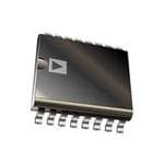
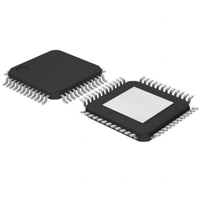
| 供应商器件封装 | 16-SSOP |
| 其它名称 | AD5933BRSZ-ND |
| 分辨率 | 12 bit |
| 分辨率(位) | 12 b |
| 功能 | Impedance measurement |
| 包装 | 管件 |
| 商标 | Analog Devices |
| 字宽调谐(位) | - |
| 安装类型 | 表面贴装 |
| 安装风格 | SMD/SMT |
| 封装 | Tube |
| 封装/外壳 | 16-SSOP(0.209",5.30mm 宽) |
| 封装/箱体 | SSOP-16 |
| 工作温度 | -40°C ~ 125°C |
| 工厂包装数量 | 77 |
| 标准包装 | 1 |
| 电压-电源 | 2.7 V ~ 5.5 V |
| 系列 | AD5933 |
| 视频文件 | http://www.digikey.cn/classic/video.aspx?PlayerID=1364138032001&width=640&height=505&videoID=2245193148001 |
| 转换器数量 | 1 |
| 转换速率 | 1 MHz |
| 配用 | /product-detail/zh/EVAL-AD5933EBZ/EVAL-AD5933EBZ-ND/1643629 |


- 商务部:美国ITC正式对集成电路等产品启动337调查
- 曝三星4nm工艺存在良率问题 高通将骁龙8 Gen1或转产台积电
- 太阳诱电将投资9.5亿元在常州建新厂生产MLCC 预计2023年完工
- 英特尔发布欧洲新工厂建设计划 深化IDM 2.0 战略
- 台积电先进制程称霸业界 有大客户加持明年业绩稳了
- 达到5530亿美元!SIA预计今年全球半导体销售额将创下新高
- 英特尔拟将自动驾驶子公司Mobileye上市 估值或超500亿美元
- 三星加码芯片和SET,合并消费电子和移动部门,撤换高东真等 CEO
- 三星电子宣布重大人事变动 还合并消费电子和移动部门
- 海关总署:前11个月进口集成电路产品价值2.52万亿元 增长14.8%


PDF Datasheet 数据手册内容提取
1 MSPS, 12-Bit Impedance Converter, Network Analyzer Data Sheet AD5933 FEATURES GENERAL DESCRIPTION Programmable output peak-to-peak excitation voltage The AD5933 is a high precision impedance converter system to a maximum frequency of 100 kHz solution that combines an on-board frequency generator with Programmable frequency sweep capability with a 12-bit, 1 MSPS, analog-to-digital converter (ADC). The serial I2C interface frequency generator allows an external complex impedance to Frequency resolution of 27 bits (<0.1 Hz) be excited with a known frequency. The response signal from Impedance measurement range from 1 kΩ to 10 MΩ the impedance is sampled by the on-board ADC and a discrete Capable of measuring of 100 Ω to 1 kΩ with additional Fourier transform (DFT) is processed by an on-board DSP circuitry engine. The DFT algorithm returns a real (R) and imaginary (I) Internal temperature sensor (±2°C) data-word at each output frequency. Internal system clock option Phase measurement capability Once calibrated, the magnitude of the impedance and relative System accuracy of 0.5% phase of the impedance at each frequency point along the sweep 2.7 V to 5.5 V power supply operation is easily calculated. This is done off chip using the real and Temperature range: −40°C to +125°C imaginary register contents, which can be read from the serial 16-lead SSOP package I2C interface. Qualified for automotive applications A similar device, also available from Analog Devices, Inc., is the APPLICATIONS AD5934, a 2.7 V to 5.5 V, 250 kSPS, 12-bit impedance converter, with an internal temperature sensor and is packaged in a 16- Electrochemical analysis lead SSOP. Bioelectrical impedance analysis Impedance spectroscopy Complex impedance measurement Corrosion monitoring and protection equipment Biomedical and automotive sensors Proximity sensing Nondestructive testing Material property analysis Fuel/battery cell condition monitoring FUNCTIONAL BLOCK DIAGRAM MCLK AVDD DVDD DDS CORE DAC OSCILLATOR (27 BITS) ROUT VOUT SCL I2C TEMPERATURE SDA INTERFACE SENSOR Z(ω) AD5933 REAL IMAGINARY RFB REGISTER REGISTER 1024-POINT DFT VIN ADC GAIN (12 BITS) LPF AGND DGND VDD/2 05324-001 Figure 1. Rev. F Document Feedback Information furnished by Analog Devices is believed to be accurate and reliable. However, no responsibility is assumed by Analog Devices for its use, nor for any infringements of patents or other One Technology Way, P.O. Box 9106, Norwood, MA 02062-9106, U.S.A. rights of third parties that may result from its use. Specifications subject to change without notice. No license is granted by implication or otherwise under any patent or patent rights of Analog Devices. Tel: 781.329.4700 ©2005–2017 Analog Devices, Inc. All rights reserved. Trademarks and registered trademarks are the property of their respective owners. Technical Support www.analog.com
AD5933 Data Sheet TABLE OF CONTENTS Features .............................................................................................. 1 Register Map ................................................................................... 23 Applications ....................................................................................... 1 Control Register (Register Address 0x80, Register Address 0x81) ............................................................................................. 23 General Description ......................................................................... 1 Functional Block Diagram .............................................................. 1 Start Frequency Register (Register Address 0x82, Register Address 0x83, Register Address 0x84) .................................... 24 Revision History ............................................................................... 3 Frequency Increment Register (Register Address 0x85, Specifications ..................................................................................... 4 Register Address 0x86, Register Address 0x87) ..................... 25 I2C Serial Interface Timing Characteristics .............................. 6 Number of Increments Register (Register Address 0x88, Absolute Maximum Ratings ............................................................ 7 Register Address 0x89) .............................................................. 25 ESD Caution .................................................................................. 7 Number of Settling Time Cycles Register (Register Address Pin Configuration and Descriptions .............................................. 8 0x8A, Register Address 0x8B) ................................................. 25 Typical Performance Characteristics ............................................. 9 Status Register (Register Address 0x8F) .................................. 26 Terminology .................................................................................... 12 Temperature Data Register (16 Bits—Register Address 0x92, Register Address 0x93) .............................................................. 26 System Description ......................................................................... 13 Real and Imaginary Data Registers (16 Bits—Register Transmit Stage ............................................................................. 14 Address 0x94, Register Address 0x95, Register Address 0x96, Frequency Sweep Command Sequence ................................... 15 Register Address 0x97) .............................................................. 26 Receive Stage ............................................................................... 15 Serial Bus Interface ......................................................................... 27 DFT Operation ........................................................................... 15 General I2C Timing .................................................................... 27 System Clock ............................................................................... 16 Writing/Reading to the AD5933 .............................................. 28 Temperature Sensor ................................................................... 16 Block Write .................................................................................. 28 Temperature Conversion Details .............................................. 16 Read Operations ......................................................................... 29 Temperature Value Register ...................................................... 16 Typical Applications ....................................................................... 30 Temperature Conversion Formula ........................................... 16 Measuring Small Impedances ................................................... 30 Impedance Calculation .................................................................. 17 Biomedical: Noninvasive Blood Impedance Measurement .. 32 Magnitude Calculation .............................................................. 17 Sensor/Complex Impedance Measurement ............................ 32 Gain Factor Calculation ............................................................ 17 Electro-Impedance Spectroscopy ............................................. 33 Impedance Calculation Using Gain Factor ............................. 17 Layout and Configuration ............................................................. 34 Gain Factor Variation with Frequency .................................... 17 Power Supply Bypassing and Grounding ................................ 34 Two-Point Calibration ............................................................... 18 Evaluation Board ............................................................................ 35 Two-Point Gain Factor Calculation ......................................... 18 Using the Evaluation Board ...................................................... 35 Gain Factor Setup Configuration ............................................. 18 Prototyping Area ........................................................................ 35 Gain Factor Recalculation ......................................................... 18 Crystal Oscillator (XO) vs. External Clock ............................. 35 Gain Factor Temperature Variation ......................................... 19 Schematics ................................................................................... 36 Impedance Error ......................................................................... 19 Outline Dimensions ....................................................................... 40 Measuring the Phase Across an Impedance ........................... 19 Ordering Guide .......................................................................... 40 Performing a Frequency Sweep .................................................... 22 Automotive Products ................................................................. 40 Rev. F | Page 2 of 40
Data Sheet AD5933 REVISION HISTORY 4/2017—Rev E to Rev F 8/2010—Rev. B to Rev. C Changes to Table 4 ............................................................................ 8 Changes to Impedance Error Section ........................................... 19 Changes to Table 12 ........................................................................ 25 Changes to Figure 45 ...................................................................... 38 Changes to U4 Description in Table 19 ....................................... 42 5/2013—Rev. D to Rev. E Added Automotive Information (Throughout) ............................ 1 2/2010—Rev. A to Rev. B Changed Sampling Rate from 250 kSPS to 1 MSPS ..................... 5 Changes to General Description ..................................................... 1 Changes to Table 7 .......................................................................... 21 Deleted Choosing a Reference for the AD5933 Section ............ 34 5/2008—Rev. 0 to Rev. A Changes to Ordering Guide ........................................................... 40 Changes to Layout .............................................................. Universal Changes to Figure 1 .......................................................................... 1 12/2011—Rev. C to Rev. D Changes to Table 1 ............................................................................ 4 Changes to Impedance Error Section ........................................... 19 Changes to Figure 17 ...................................................................... 13 Removed Figure 26 and Figure 27; Changes to System Description Section....................................... 13 Renumbered Sequentially .............................................................. 19 Changes to Figure 19 ...................................................................... 14 Removed Figure 28, Figure 29, Figure 30, Figure 31 .................. 20 Changes to Figure 24 ...................................................................... 18 Changes to Figure 39 ...................................................................... 37 Changes to Impedance Error Section ........................................... 19 Changes to Figure 40 ...................................................................... 38 Added Measuring the Phase Across an Impedance Section ..... 21 Changes to Figure 41 ...................................................................... 39 Changes to Register Map Section ................................................. 24 Changes to Figure 42 ...................................................................... 40 Added Measuring Small Impedances Section ............................. 31 Changes to Table 18 ........................................................................ 35 Added Evaluation Board Section .................................................. 37 Changes to Ordering Guide ........................................................... 43 9/2005—Revision 0: Initial Version Rev. F | Page 3 of 40
AD5933 Data Sheet SPECIFICATIONS VDD = 3.3 V, MCLK = 16.776 MHz, 2 V p-p output excitation voltage @ 30 kHz, 200 kΩ connected between Pin 5 and Pin 6; feedback resistor = 200 kΩ connected between Pin 4 and Pin 5; PGA gain = ×1, unless otherwise noted. Table 1. Y Version1 Parameter Min Typ Max Unit Test Conditions/Comments SYSTEM Impedance Range 1 K 10 M Ω 100 Ω to 1 kΩ requires extra buffer circuitry, see the Measuring Small Impedances section Total System Accuracy 0.5 % 2 V p-p output excitation voltage at 30 kHz, 200 kΩ connected between Pin 5 and Pin 6 System Impedance Error Drift 30 ppm/°C TRANSMIT STAGE Output Frequency Range2 1 100 kHz Output Frequency Resolution 0.1 Hz <0.1 Hz resolution achievable using DDS techniques MCLK Frequency 16.776 MHz Maximum system clock frequency Internal Oscillator Frequency3 16.776 MHz Frequency of internal clock Internal Oscillator Temperature Coefficient 30 ppm/°C TRANSMIT OUTPUT VOLTAGE Range 1 AC Output Excitation Voltage4 1.98 V p-p See Figure 4 for output voltage distribution DC Bias5 1.48 V DC bias of the ac excitation signal; see Figure 5 DC Output Impedance 200 Ω T = 25°C A Short-Circuit Current to Ground at VOUT ±5.8 mA T = 25°C A Range 2 AC Output Excitation Voltage4 0.97 V p-p See Figure 6 DC Bias5 0.76 V DC bias of output excitation signal; see Figure 7 DC Output Impedance 2.4 kΩ Short-Circuit Current to Ground at VOUT ±0.25 mA Range 3 AC Output Excitation Voltage4 0.383 V p-p See Figure 8 DC Bias5 0.31 V DC bias of output excitation signal; see Figure 9 DC Output Impedance 1 kΩ Short-Circuit Current to Ground at VOUT ±0.20 mA Range 4 AC Output Excitation Voltage4 0.198 V p-p See Figure 10 DC Bias5 0.173 V DC bias of output excitation signal. See Figure 11 DC Output Impedance 600 Ω Short-Circuit Current to Ground at VOUT ±0.15 mA SYSTEM AC CHARACTERISTICS Signal-to-Noise Ratio 60 dB Total Harmonic Distortion −52 dB Spurious-Free Dynamic Range Wide Band (0 MHz to 1 MHz) −56 dB Narrow Band (±5 kHz) −85 dB Rev. F | Page 4 of 40
Data Sheet AD5933 Y Version1 Parameter Min Typ Max Unit Test Conditions/Comments RECEIVE STAGE Input Leakage Current 1 nA To VIN pin Input Capacitance6 0.01 pF Pin capacitance between VIN and GND Feedback Capacitance (C ) 3 pF Feedback capacitance around current- FB to-voltage amplifier; appears in parallel with feedback resistor ANALOG-TO-DIGITAL CONVERTER6 Resolution 12 Bits Sampling Rate 1 MSPS ADC throughput rate TEMPERATURE SENSOR Accuracy ±2.0 °C −40°C to +125°C temperature range Resolution 0.03 °C Temperature Conversion Time 800 μs Conversion time of single temperature measurement LOGIC INPUTS Input High Voltage (V ) 0.7 × VDD IH Input Low Voltage (V ) 0.3 × VDD IL Input Current7 1 µA T = 25°C A Input Capacitance 7 pF T = 25°C A POWER REQUIREMENTS VDD 2.7 5.5 V IDD (Normal Mode ) 10 15 mA VDD = 3.3 V 17 25 mA VDD = 5.5 V IDD (Standby Mode) 11 mA VDD = 3.3 V; see the Control Register (Register Address 0X80, Register Address 0X81) section 16 mA VDD = 5.5 V IDD (Power-Down Mode) 0.7 5 µA VDD = 3.3 V 1 8 µA VDD = 5.5 V 1 Temperature range for Y version = −40°C to +125°C, typical at 25°C. 2 The lower limit of the output excitation frequency can be lowered by scaling the clock supplied to the AD5933. 3 Refer to Figure 14, Figure 15, and Figure 16 for the internal oscillator frequency distribution with temperature. 4 The peak-to-peak value of the ac output excitation voltage scales with supply voltage according to the following formula: Output Excitation Voltage (V p-p) = [2/3.3] × VDD where VDD is the supply voltage. 5 The dc bias value of the output excitation voltage scales with supply voltage according to the following formula: Output Excitation Bias Voltage (V) = [2/3.3] × VDD where VDD is the supply voltage. 6 Guaranteed by design or characterization, not production tested. Input capacitance at the VOUT pin is equal to pin capacitance divided by open-loop gain of current- to-voltage amplifier. 7 The accumulation of the currents into Pin 8, Pin 15, and Pin 16. Rev. F | Page 5 of 40
AD5933 Data Sheet I2C SERIAL INTERFACE TIMING CHARACTERISTICS VDD = 2.7 V to 5.5 V. All specifications T to T , unless otherwise noted.1 MIN MAX Table 2. Parameter2 Limit at T , T Unit Description MIN MAX f 400 kHz max SCL clock frequency SCL t 2.5 µs min SCL cycle time 1 t 0.6 µs min t , SCL high time 2 HIGH t 1.3 µs min t , SCL low time 3 LOW t 0.6 µs min t , start/repeated start condition hold time 4 HD, STA t 100 ns min t , data setup time 5 SU, DAT t 3 0.9 µs max t , data hold time 6 HD, DAT 0 µs min t , data hold time HD, DAT t 0.6 µs min t , setup time for repeated start 7 SU, STA t 0.6 µs min t , stop condition setup time 8 SU, STO t 1.3 µs min t , bus free time between a stop and a start condition 9 BUF t 300 ns max t, rise time of SDA when transmitting 10 F 0 ns min t , rise time of SCL and SDA when receiving (CMOS compatible) R t 300 ns max t, fall time of SCL and SDA when transmitting 11 F 0 ns min t, fall time of SDA when receiving (CMOS compatible) F 250 ns max t, fall time of SDA when receiving F 20 + 0.1 C 4 ns min t, fall time of SCL and SDA when transmitting b F C 400 pF max Capacitive load for each bus line b 1 See Figure 2. 2 Guaranteed by design and characterization, not production tested. 3 A master device must provide a hold time of at least 300 ns for the SDA signal (referred to VIH MIN of the SCL signal) to bridge the undefined falling edge of SCL. 4 Cb is the total capacitance of one bus line in picofarads. Note that tR and tF are measured between 0.3 VDD and 0.7 VDD. SDA t9 t3 t10 t11 t4 SCL t4 t6 t2 t5 t7 t1 t8 COSNTDAIRTTION CROESPNTEDAAIRTTTIEODN COSNTDOITPION 05324-002 Figure 2. I2C Interface Timing Diagram Rev. F | Page 6 of 40
Data Sheet AD5933 ABSOLUTE MAXIMUM RATINGS T = 25°C, unless otherwise noted. A Table 3. Stresses at or above those listed under Absolute Maximum Parameter Rating Ratings may cause permanent damage to the product. This is a DVDD to GND −0.3 V to +7.0 V stress rating only; functional operation of the product at these AVDD1 to GND −0.3 V to +7.0 V or any other conditions above those indicated in the operational AVDD2 to GND −0.3 V to +7.0 V section of this specification is not implied. Operation beyond SDA/SCL to GND −0.3 V to VDD + 0.3 V the maximum operating conditions for extended periods may VOUT to GND −0.3 V to VDD + 0.3 V affect product reliability. VIN to GND −0.3 V to VDD + 0.3 V MCLK to GND −0.3 V to VDD + 0.3 V ESD CAUTION Operating Temperature Range Extended Industrial (Y Grade) −40°C to +125°C Storage Temperature Range −65°C to +160°C Maximum Junction Temperature 150°C SSOP Package, Thermal Impedance θ 139°C/W JA θ 136°C/W JC Reflow Soldering (Pb-Free) Peak Temperature 260°C Time at Peak Temperature 10 sec to 40 sec Rev. F | Page 7 of 40
AD5933 Data Sheet PIN CONFIGURATION AND DESCRIPTIONS NC 1 16 SCL NC 2 15 SDA NC 3 14 AGND2 AD5933 RFB 4 13 AGND1 TOP VIEW VIN 5 (Not to Scale) 12 DGND VOUT 6 11 AVDD2 NC 7 10 AVDD1 MCLK 8 9 DVDD NC = NO CONNECT NOTES: 1.IT IS RECOMMENDEDTO TIEALL SUPPLY CONNECTIONS (PIN 9, PIN 10,AND PIN11) AND RUN FROM A SINGLE SUPPLY BETWEEN 2C(P.O7INVN N1A2EN,C DPT I5NA.5 L1V3L. , IGATR NISODA UPLNINSD O 1S 4RI)G.ENCAOLMSMTEONGDEETDHTEOR 05324-003 Figure 3. Pin Configuration Table 4. Pin Function Descriptions Pin No. Mnemonic Description 1, 2, 3, 7 NC No Connect. Do not connect to this pin. 4 RFB External Feedback Resistor. Connected from Pin 4 to Pin 5 and used to set the gain of the current-to-voltage amplifier on the receive side. 5 VIN Input to Receive Transimpedance Amplifier. Presents a virtual earth voltage of VDD/2. 6 VOUT Excitation Voltage Signal Output. 8 MCLK The master clock for the system is supplied by the user. 9 DVDD Digital Supply Voltage. 10 AVDD1 Analog Supply Voltage 1. 11 AVDD2 Analog Supply Voltage 2. 12 DGND Digital Ground. 13 AGND1 Analog Ground 1. 14 AGND2 Analog Ground 2. 15 SDA I2C Data Input. Open-drain pins requiring 10 kΩ pull-up resistors to VDD. 16 SCL I2C Clock Input. Open-drain pins requiring 10 kΩ pull-up resistors to VDD. Rev. F | Page 8 of 40
Data Sheet AD5933 TYPICAL PERFORMANCE CHARACTERISTICS 35 30 MEAN = 1.9824 MEAN = 0.7543 SIGMA = 0.0072 SIGMA = 0.0099 30 25 S 25 S CE CE 20 VI VI DE 20 DE OF OF 15 ER 15 ER B B M M U U 10 N 10 N 5 5 01.92 1.94 1.96 V1.O98LTAGE2 .(0V0) 2.02 2.04 2.06 05324-004 00.68 0.70 0.72 0.74 V0O.7L6TAG0E.7 (8V) 0.80 0.82 0.84 0.86 05324-007 Figure 4. Range 1 Output Excitation Voltage Distribution, VDD = 3.3 V Figure 7. Range 2 DC Bias Distribution, VDD = 3.3 V 30 30 MEAN = 1.4807 MEAN = 0.3827 SIGMA = 0.0252 SIGMA = 0.00167 25 25 S S CE 20 CE 20 VI VI E E D D OF 15 OF 15 R R E E B B UM 10 UM 10 N N 5 5 01.30 1.35 1.40 1.45 V1O.5L0TAG1E.5 (5V) 1.60 1.65 1.70 1.75 05324-005 00.370 0.375 0.380 VOL0T.A3G85E (V) 0.390 0.395 0.400 05324-008 Figure 5. Range 1 DC Bias Distribution, VDD = 3.3 V Figure 8. Range 3 Output Excitation Voltage Distribution, VDD = 3.3 V 30 30 MEAN = 0.9862 MEAN = 0.3092 SIGMA = 0.0041 SIGMA = 0.0014 25 25 NUMBER OF DEVICES 211050 NUMBER OF DEVICES 121050 5 5 00.95 0.96 0.97 V0.O98LTAGE0 .(9V9) 1.00 1.01 1.02 05324-006 00.290 0.295 0.300 VOL0T.A3G05E (V) 0.310 0.315 0.320 05324-009 Figure 6. Range 2 Output Excitation Voltage Distribution, VDD = 3.3 V Figure 9. Range 3 DC Bias Distribution, VDD = 3.3 V Rev. F | Page 9 of 40
AD5933 Data Sheet 30 15.8 MEAN = 0.1982 AVDD1,AVDD2, DVDD CONNECTEDTOGETHER. SIGMA = 0.0008 15.3 OUTPUT EXCITATION FREQUENCY = 30kHz 25 RFB, ZCALIBRATION = 100kΩ 14.8 CES 20 14.3 DEVI A) 13.8 R OF 15 DD (m 13.3 BE I 12.8 M U 10 N 12.3 11.8 5 11.3 00.192 0.194 0.196 0V.1O9L8TAGE0. 2(V00) 0.202 0.204 0.206 05324-010 10.80 2 4 MC6LK FR8EQUE1N0CY (M1H2z) 14 16 18 05324-012 Figure 10. Range 4 Output Excitation Voltage Distribution, VDD = 3.3 V Figure 12. Typical Supply Current vs. MCLK Frequency 30 0.4 MEAN = 0.1792 VDD = 3.3V SIGMA = 0.0024 TA = 25°C 0.2 f = 32kHz 25 S es) 0 ER OF DEVICE 2105 ERROR (Degre ––00..24 UMB 10 ASE N H –0.6 P 5 –0.8 00.160 0.165 0.170 0.175 V0O.1L8T0AG0E.1 8(V5) 0.190 0.195 0.200 0.205 05324-011 –1.00 50 100 1P5H0ASE2 (0D0egree2s5)0 300 350 400 05324-013 Figure 11. Range 4 DC Bias Distribution, VDD = 3.3 V Figure 13. Typical Phase Error Rev. F | Page 10 of 40
Data Sheet AD5933 N = 106 12 N = 100 12 MEAN = 16.8292 MEAN = 16.7257 SD = 0.142904 SD = 0.137633 TEMP = –40°C 10 TEMP = 125°C 10 8 8 T T N N OU OU 6 C 6 C 4 4 2 2 0 0 16.4 OS1C6.I6LLATOR FR1E6Q.8UENCY (MH17z.)0 17.2 05324-014 16.4 OS1C6.I6LLATOR FR1E6Q.8UENCY (MH17z.)0 17.2 05324-016 Figure 14. Frequency Distribution of Internal Oscillator at −40°C Figure 16. Frequency Distribution of Internal Oscillator at 125°C 16 N = 100 MEAN = 16.7811 SD = 0.0881565 14 TEMP = 25°C 12 10 T N OU 8 C 6 4 2 0 16.4 OS1C6.I6LLATOR FR1E6Q.8UENCY (MH17z.)0 17.2 05324-015 Figure 15. Frequency Distribution of Internal Oscillator at 25°C Rev. F | Page 11 of 40
AD5933 Data Sheet TERMINOLOGY Total System Accuracy Signal-to-Noise Ratio (SNR) The AD5933 can accurately measure a range of impedance SNR is the ratio of the rms value of the measured output signal values to less than 0.5% of the correct impedance value for to the rms sum of all other spectral components below the supply voltages between 2.7 V to 5.5 V. Nyquist frequency. The value for SNR is expressed in decibels. Spurious-Free Dynamic Range (SFDR) Total Harmonic Distortion (THD) Along with the frequency of interest, harmonics of the funda- THD is the ratio of the rms sum of harmonics to the funda- mental frequency and images of these frequencies are present at mental, where V1 is the rms amplitude of the fundamental the output of a DDS device. The spurious-free dynamic range and V2, V3, V4, V5, and V6 are the rms amplitudes of the refers to the largest spur or harmonic present in the band of second through the sixth harmonics. For the AD5933, THD interest. The wideband SFDR gives the magnitude of the largest is defined as harmonic or spur relative to the magnitude of the fundamental frequency in the 0 Hz to Nyquist bandwidth. The narrow-band V22 +V32 +V42 +V52V62 SFDR gives the attenuation of the largest spur or harmonic in a THD(dB)=20log V1 bandwidth of ±200 kHz, about the fundamental frequency. Rev. F | Page 12 of 40
Data Sheet AD5933 SYSTEM DESCRIPTION MCLK DDS CORE DAC OSCILLATOR (27 BITS) COS SIN ROUT VOUT SCL I2C TEMPERATURE MICROCONTROLLER INTERFACE SENSOR SDA Z(ω) REAL IMAGINARY AD5933 REGISTER REGISTER MAC CORE RFB (1024 DFT) PROGRAMMABLE WINDOWING MCLK GAINAMPLIFIER OF DATA VIN ADC ×5 (12 BITS) LPF ×1 VDD/2 05324-017 Figure 17. Block Overview The AD5933 is a high precision impedance converter system The AD5933 permits the user to perform a frequency sweep with solution that combines an on-board frequency generator with a a user-defined start frequency, frequency resolution, and number 12-bit, 1 MSPS ADC. The frequency generator allows an external of points in the sweep. In addition, the device allows the user to complex impedance to be excited with a known frequency. The program the peak-to-peak value of the output sinusoidal signal as response signal from the impedance is sampled by the on-board an excitation to the external unknown impedance connected ADC and DFT processed by an on-board DSP engine. The DFT between the VOUT and VIN pins. algorithm returns both a real (R) and imaginary (I) data-word at Table 5 gives the four possible output peak-to-peak voltages and each frequency point along the sweep. The impedance magnitude the corresponding dc bias levels for each range for 3.3 V. These and phase are easily calculated using the following equations: values are ratiometric with VDD. So for a 5 V supply Magnitude= R2 +I2 OutputExcitationVoltage forRange1=1.98 × 5.0 =3Vp−p 3.3 Phase = tan−1(I/R) 5.0 OutputDCBiasVoltage forRange1=1.48× =2.24Vp−p To characterize an impedance profile Z(ω), generally a frequency 3.3 sweep is required, like that shown in Figure 18. Table 5. Voltage Levels Respective Bias Levels for 3.3 V Output Excitation Range Voltage Amplitude Output DC Bias Level 1 1.98 V p-p 1.48 V 2 0.97 V p-p 0.76 V E 3 383 mV p-p 0.31 V C N 4 198 mV p-p 0.173 V A D E MP The excitation signal for the transmit stage is provided on-chip I using DDS techniques that permit subhertz resolution. The receive stage receives the input signal current from the unknown impedance, performs signal processing, and digitizes the result. The clock for the DDS is generated from either an external reference clock, FREQUENCY 05324-018 woshciicllha tios rp. rTohveid celodc bky f othr et hues eDr DatS M isC dLeKte,r omr ibnye dth bey i nthteer sntaatl us of Figure 18. Impedance vs. Frequency Profile Bit D3 in the control register (see Register Address 0x81 in the Register Map section). Rev. F | Page 13 of 40
AD5933 Data Sheet TRANSMIT STAGE Frequency Increment As shown in Figure 19, the transmit stage of the AD5933 is made This is a 24-bit word that is programmed to the on-board RAM up of a 27-bit phase accumulator DDS core that provides the at Register Address 0x85, Register Address 0x86, and Register output excitation signal at a particular frequency. The input to Address 0x87 (see the Register Map). The required code loaded the phase accumulator is taken from the contents of the start to the frequency increment register is the result of the formula frequency register (see Register Address 0x82, Register Address shown in Equation 2, based on the master clock frequency and the 0x83, and Register Address 0x84). Although the phase accumu- required increment frequency output from the DDS. lator offers 27 bits of resolution, the start frequency register has FrequencyIncrementCode= the three most significant bits (MSBs) set to 0 internally; therefore, the user has the ability to program only the lower 24 bits of the start frequency register. RequiredFrequencyIncrement×227 (2) MCLK R(GAIN) 4 PHASE ACC(2U7M BUILTAST)OR DAC VBIAS VOUT 05324-019 Fofo r1 0e xHamz apnled, hifa tsh ae 1u6s eMr rHeqz ucilroecsk t hsieg nswale ceopn tnoe hcatevde ato r eMsoCluLtKio, nth e Figure 19. Transmit Stage code that needs to be programmed is given by The AD5933 offers a frequency resolution programmable by the user down to 0.1 Hz. The frequency resolution is programmed 10Hz via a 24-bit word loaded serially over the I2C interface to the FrequencyIncrementCode=16MHz≡0x00014F frequency increment register. 4 The frequency sweep is fully described by the programming of The user programs the value of 0x00 to Register Address 0x85, three parameters: the start frequency, the frequency increment, the value of 0x01 to Register Address 0x86, and the value of 0x4F and the number of increments. to Register Address 0x87. Start Frequency Number of Increments This is a 24-bit word that is programmed to the on-board RAM This is a 9-bit word that represents the number of frequency at Register Address 0x82, Register Address 0x83, and Register points in the sweep. The number is programmed to the on-board Address 0x84 (see the Register Map section). The required code RAM at Register Address 0x88 and Register Address 0x89 (see the loaded to the start frequency register is the result of the formula Register Map section). The maximum number of points that can shown in Equation 1, based on the master clock frequency and the be programmed is 511. required start frequency output from the DDS. For example, if the sweep needs 150 points, the user programs StartFrequencyCode= the value of 0x00 to Register Address 0x88 and the value of 0x96 to Register Address 0x89. RequiredOutputStartFrequency×227 (1) Once the three parameter values have been programmed, the MCLK sweep is initiated by issuing a start frequency sweep command to 4 the control register at Register Address 0x80 and Register Address 0x81 (see the Register Map section). Bit D2 in the status register For example, if the user requires the sweep to begin at 30 kHz and (Register Address 0x8F) indicates the completion of the frequency has a 16 MHz clock signal connected to MCLK, the code that measurement for each sweep point. Incrementing to the next needs to be programmed is given by frequency sweep point is under the control of the user. The measured result is stored in the two register groups that follow: 30kHz 0x94, 0x95 (real data) and 0x96, 0x97 (imaginary data) that should StartFrequencyCode= ×227 ≡0x0F5C28 16MHz be read before issuing an increment frequency command to the control register to move to the next sweep point. There is the 4 facility to repeat the current frequency point measurement by The user programs the value of 0x0F to Register Address 0x82, the issuing a repeat frequency command to the control register. This value of 0x5C to Register Address 0x83, and the value of 0x28 to has the benefit of allowing the user to average successive readings. Register Address 0x84. When the frequency sweep has completed all frequency points, Bit D3 in the status register is set, indicating completion of the sweep. Once this bit is set, further increments are disabled. Rev. F | Page 14 of 40
Data Sheet AD5933 FREQUENCY SWEEP COMMAND SEQUENCE RECEIVE STAGE The following sequence must be followed to implement a The receive stage comprises a current-to-voltage amplifier, frequency sweep: followed by a programmable gain amplifier (PGA), antialiasing filter, and ADC. The receive stage schematic is shown in 1. Enter standby mode. Prior to issuing a start frequency sweep Figure 20. The unknown impedance is connected between the command, the device must be placed in a standby mode by VOUT and VIN pins. The first stage current-to-voltage amplifier issuing an enter standby mode command to the control configuration means that a voltage present at the VIN pin is a register (Register Address 0x80 and Register Address 0x81). virtual ground with a dc value set at VDD/2. The signal current In this mode, the VOUT and VIN pins are connected that is developed across the unknown impedance flows into the internally to ground so there is no dc bias across the external VIN pin and develops a voltage signal at the output of the current- impedance or between the impedance and ground. to-voltage converter. The gain of the current-to voltage amplifier 2. Enter initialize mode. In general, high Q complex circuits is determined by a user-selectable feedback resistor connected require a long time to reach steady state. To facilitate the between Pin 4 (RFB) and Pin 5 (VIN). It is important for the user measurement of such impedances, this mode allows the user to choose a feedback resistance value that, in conjunction with the full control of the settling time requirement before entering selected gain of the PGA stage, maintains the signal within the start frequency sweep mode where the impedance linear range of the ADC (0 V to VDD). measurement takes place. An initialize with a start frequency command to the control The PGA allows the user to gain the output of the current-to- register enters initialize mode. In this mode the impedance voltage amplifier by a factor of 5 or 1, depending upon the status is excited with the programmed start frequency, but no meas- of Bit D8 in the control register (see the Register Map section, urement takes place. The user times out the required settling Register Address 0x80). The signal is then low-pass filtered and time before issuing a start frequency sweep command to the presented to the input of the 12-bit, 1 MSPS ADC. control register to enter the start frequency sweep mode. R RFB 3. Enter start frequency sweep mode. The user enters this mode 5 × R C by issuing a start frequency sweep command to the control R register. In this mode, the ADC starts measuring after the programmed number of settling time cycles has elapsed. The VIN R user can program an integer number of output frequency Rcyecgliesst e(rs eAttdlidnrge stsim 0xe8 cBy cbleesfo) rteo bReegginisnteinr gA tdhder emsse a0sxu8rAem anendt VDD/2 LPF ADC 05324-020 Figure 20. Receive Stage at each frequency point (see Figure 28). The digital data from the ADC is passed directly to the DSP core The DDS output signal is passed through a programmable gain of the AD5933, which performs a DFT on the sampled data. stage to generate the four ranges of peak-to-peak output excitation DFT OPERATION signals listed in Table 5. The peak-to-peak output excitation volt- age is selected by setting Bit D10 and Bit D9 in the control register A DFT is calculated for each frequency point in the sweep. The (see the Control Register (Register Address 0X80, Register AD5933 DFT algorithm is represented by Address 0X81) section) and is made available at the VOUT pin. 1023 X(f)= ∑(x(n)(cos(n)−jsin(n))) n=0 where: X(f) is the power in the signal at the Frequency Point f. x(n) is the ADC output. cos(n) and sin(n) are the sampled test vectors provided by the DDS core at the Frequency Point f. The multiplication is accumulated over 1024 samples for each frequency point. The result is stored in two, 16-bit registers representing the real and imaginary components of the result. The data is stored in twos complement format. Rev. F | Page 15 of 40
AD5933 Data Sheet SYSTEM CLOCK Table 6. Temperature Data Format Temperature Digital Output D13…D0 The system clock for the AD5933 can be provided in one of two ways. The user can provide a highly accurate and stable system −40°C 11, 1011, 0000, 0000 clock at the external clock pin (MCLK). Alternatively, the AD5933 −30°C 11, 1100, 0100, 0000 provides an internal clock with a typical frequency of 16.776 MHz −25°C 11, 1100, 1110, 0000 by means of an on-chip oscillator. −10°C 11, 1110, 1100, 0000 −0.03125°C 11, 1111, 1111, 1111 The user can select the preferred system clock by programming 0°C 00, 0000, 0000, 0000 Bit D3 in the control register (Register Address 0x81, see +0.03125°C 00, 0000, 0000, 0001 Table 11). The default clock option on power-up is selected to +10°C 00, 0001, 0100, 0000 be the internal oscillator. +25°C 00, 0011, 0010, 0000 The frequency distribution of the internal clock with temperature +50°C 00, 0110, 0100, 0000 can be seen in Figure 14, Figure 15, and Figure 16. +75°C 00, 1001, 0110, 0000 TEMPERATURE SENSOR +100°C 00, 1100, 1000, 0000 +125°C 00, 1111, 1010, 0000 The temperature sensor is a 13-bit digital temperature sensor with +150°C 01, 0010, 1100, 0000 a 14th bit that acts as a sign bit. The on-chip temperature sensor allows an accurate measurement of the ambient device temper- ature to be made. TEMPERATURE CONVERSION FORMULA The measurement range of the sensor is −40°C to +125°C. At Positive Temperature = ADC Code (D)/32 +150°C, the structural integrity of the device starts to deteriorate Negative Temperature = (ADC Code (D) – 16384)/32 when operated at voltage and temperature maximum specifica- where ADC Code uses all 14 bits of the data byte, including the tions. The accuracy within the measurement range is ±2°C. sign bit. TEMPERATURE CONVERSION DETAILS Negative Temperature = (ADC Code (D) – 8192)/32 The conversion clock for the part is internally generated; no where ADC Code (D) is D13, the sign bit, and is removed from the external clock is required except when reading from and writing ADC code.) to the serial port. In normal mode, an internal clock oscillator 01, 0010,1100, 0000 runs an automatic conversion sequence. The temperature sensor block defaults to a power-down state. T To perform a measurement, a measure temperature command U P T is issued by the user to the control register (Register Address 0x80 U O and Register Address 0x81). After the temperature operation is AL T complete (typically 800 μs later), the block automatically 00, 1001, 0110, 0000 DIGI 75°C powers down until the next temperature command is issued. The user can poll the status register (Register Address 0x8F) to see if a valid temperature conversion has taken place, indicating that 00, 0000, 0000, 0001 valid temperature data is available to read at Register Address 0x92 and Register Address 0x93 (see the Register Map section). –0.03125°C 11,1111,1111,1111 TEMPERATURE (°C) –40°C 150°C TEMPERATURE VALUE REGISTER –30°C 11,1100, 0100, 0000 The temperature value register is a 16-bit, read-only register that sctoomrepsl ethmee tnetm fopremraatut.r Te hreea tdwino gM frSoBm b itthse a AreD dCon i’nt c1a4r-ebsi.t D, t1w3o iss the 11, 1011, 0000, 0000 05324-021 sign bit. The internal temperature sensor is guaranteed to a low Figure 21. Temperature Sensor Transfer Function value limit of –40°C and a high value limit of +150°C. The digital output stored in Register Address 0x92 and Register Address 0x93 for the various temperatures is outlined in Table 6. The tempera- ture sensor transfer characteristic is shown in Figure 21. Rev. F | Page 16 of 40
Data Sheet AD5933 IMPEDANCE CALCULATION MAGNITUDE CALCULATION 1 200kΩ The first step in impedance calculation for each frequency point GainFactor= =515.819 × 10⁻¹² is to calculate the magnitude of the DFT at that point. 9692.106 The DFT magnitude is given by IMPEDANCE CALCULATION USING GAIN FACTOR Magnitude= R2 +I2 The next example illustrates how the calculated gain factor where: derived previously is used to measure an unknown impedance. R is the real number stored at Register Address 0x94 and For this example, assume that the unknown impedance = 510 Register Address 0x95. kΩ. I is the imaginary number stored at Register Address 0x96 and After measuring the unknown impedance at a frequency of Register Address 0x97. 30 kHz, assume that the real data and imaginary data registers For example, assume the results in the real data and imaginary contain the following data: data registers are as follows at a frequency point: Real data register = 0xFA3F = −1473 decimal Real data register = 0x038B = 907 decimal Imaginary data register = 0x0DB3 = +3507 decimal Imaginary data register = 0x0204 = 516 decimal Magnitude= ((−1473)2 +(3507)2)=3802.863 Magnitude= (9072 +5162)=1043.506 Then the measured impedance at the frequency point is given To convert this number into impedance, it must be multiplied by by 1 a scaling factor called the gain factor. The gain factor is = GainFactor×Magnitude calculated during the calibration of the system with a known Impedance impedance connected between the VOUT and VIN pins. 1 = Ω=509.791kΩ Once the gain factor has been calculated, it can be used in the 515.819273×10−12×3802.863 calculation of any unknown impedance between the VOUT and VIN pins. GAIN FACTOR VARIATION WITH FREQUENCY GAIN FACTOR CALCULATION Because the AD5933 has a finite frequency response, the gain An example of a gain factor calculation follows, with the factor also shows a variation with frequency. This variation in following assumptions: gain factor results in an error in the impedance calculation over Output excitation voltage = 2 V p-p a frequency range. Figure 22 shows an impedance profile based on a single-point gain factor calculation. To minimize this error, Calibration impedance value, Z = 200 kΩ CALIBRATION the frequency sweep should be limited to as small a frequency PGA Gain = ×1 range as possible. Current-to-voltage amplifier gain resistor = 200 kΩ 101.5 VDD = 3.3V Calibration frequency = 30 kHz CALIBRATION FREQUENCY = 60kHz 101.0 TA = 25°C Then typical contents of the real data and imaginary data MEASURED CALIBRATION IMPEDANCE = 100kΩ registers after a frequency point conversion are: Ω) 100.5 k Real data register = 0xF064 = −3996 decimal E ( C N 100.0 Imaginary data register = 0x227E = +8830 decimal A D E P M Magnitude= (−3996)2 +(8830)2 =9692.106 I 99.5 1 99.0 Admittance Impedance GainFactor= = 98.5 Code Magnitude 54 56 58FREQUE6N0CY (kHz)62 64 66 05324-022 Figure 22. Impedance Profile Using a Single-Point Gain Factor Calculation Rev. F | Page 17 of 40
AD5933 Data Sheet TWO-POINT CALIBRATION GAIN FACTOR SETUP CONFIGURATION Alternatively, it is possible to minimize this error by assuming When calculating the gain factor, it is important that the receive that the frequency variation is linear and adjusting the gain stage operate in its linear region. This requires careful selection factor with a two-point calibration. Figure 23 shows an of the excitation signal range, current-to-voltage gain resistor, impedance profile based on a two-point gain factor calculation. and PGA gain. 101.5 CURRENT-TO-VOLTAGE VDD = 3.3V GAIN SETTING RESISTOR CALIBRATION FREQUENCY = 60kHz 101.0 TA = 25°C RFB MEASURED CALIBRATION IMPEDANCE = 100kΩ ZUNKNOWN Ω) 100.5 VOUT ANCE (k 100.0 VDDV/2IN (×1P OGRA ×5) LPF ADC 05324-024 D E Figure 24. System Voltage Gain P M I 99.5 The gain through the system shown in Figure 24 is given by 99.0 OuputExcitationVoltageRange× 98.554 56 58FREQUE6N0CY (kHz)62 64 66 05324-023 GainSZettingResistor ×PGAGain UNKNOWN Figure 23. Impedance Profile Using a Two-Point Gain Factor Calculation For this example, assume the following system settings: TWO-POINT GAIN FACTOR CALCULATION VDD = 3.3 V This is an example of a two-point gain factor calculation Gain setting resistor = 200 kΩ assuming the following: Z = 200 kΩ Output excitation voltage = 2 V (p-p) UNKNOWN PGA setting = ×1 Calibration impedance value, Z = 100.0 kΩ UNKNOWN The peak-to-peak voltage presented to the ADC input is PGA gain = ×1 2 V p-p. However, if a PGA gain of ×5 was chose, the voltage Supply voltage = 3.3 V would saturate the ADC. Current-to-voltage amplifier gain resistor = 100 kΩ GAIN FACTOR RECALCULATION Calibration frequencies = 55 kHz and 65 kHz The gain factor must be recalculated for a change in any of the Typical values of the gain factor calculated at the two calibration following parameters: frequencies read • Current-to-voltage gain setting resistor Gain factor calculated at 55 kHz is 1.031224E-09 • Output excitation voltage Gain factor calculated at 65 kHz is 1.035682E-09 • PGA gain Difference in gain factor (∆GF) is 1.035682E-09 − 1.031224E-09 = 4.458000E-12 Frequency span of sweep (∆F) = 10 kHz Therefore, the gain factor required at 60 kHz is given by 4.458000E-12 ×5kHz+1.031224×10⁻⁹ 10kHz The required gain factor is 1.033453E-9. The impedance is calculated as previously described. Rev. F | Page 18 of 40
Data Sheet AD5933 GAIN FACTOR TEMPERATURE VARIATION by calculating the magnitude of the real and imaginary compo- nents of the DFT given by the following formula: The typical impedance error variation with temperature is in the order of 30 ppm/°C. Figure 25 shows an impedance profile Magnitude= R2 +I2 with a variation in temperature for 100 kΩ impedance using a two-point gain factor calibration. After each measurement, multiply it by the calibration term and 101.5 invert the product. The magnitude of the impedance is, therefore, VDD = 3.3V CALIBRATION FREQUENCY = 60kHz given by the following formula: MEASURED CALIBRATION IMPEDANCE = 100kΩ 101.0 1 Impedance= +125°C GainFactor×Magnitude Ω) 100.5 k E ( Where gain factor is given by C N 100.0 A IMPED 99.5 +25°C Admittance Impe1dance –40°C GainFactor= = Code Magnitude 99.0 The user must calibrate the AD5933 system for a known impedance range to determine the gain factor before any valid 98.554 56 58FREQUE6N0CY (kHz)62 64 66 05324-025 mimepaesduarenmcee lnimt ciatsn otfa kthe ep claocme.p Tlehxe irmefporeed,a tnhcee u (sZeUrN mKNuOsWtN k)n foorw t hthee Figure 25. Impedance Profile Variation with Temperature Using a Two-Point sweep frequency range of interest. The gain factor is determined Gain Factor Calibration by placing a known impedance between the input/output of the IMPEDANCE ERROR AD5933 and measuring the resulting magnitude of the code. It is important when reading the following section to note that The AD5933 system gain settings need to be chosen to place the excitation signal in the linear region of the on-board ADC. the output impedance associated with the excitation voltages was actually measured and then calibrated out for each Because the AD5933 returns a complex output code made up of impedance error measurement. This was done using a Keithley real and imaginary components, the user can also calculate the current source/sink and measuring the voltage. phase of the response signal through the AD5933 signal path. The phase is given by the following formula: R (for example ,200 Ω specified for a 1.98 V p-p in the OUT specification table) is only a typical specification and can vary Phase(rads) = tan−1(I/R) (3) from part to part. This method may not be achievable for large The phase measured by Equation 3 accounts for the phase shift volume applications and in such cases, it is advised to use an introduced to the DDS output signal as it passes through the extra low impedance output amplifier, as shown in Figure 4, to internal amplifiers on the transmit and receive side of the improve accuracy. AD5933 along with the low-pass filter and also the impedance Please refer to CN-0217 for impedance accuracy examples on connected between the VOUT and VIN pins of the AD5933. the AD5933 product web-page. The parameters of interest for many users are the magnitude of MEASURING THE PHASE ACROSS AN IMPEDANCE the impedance (|Z |) and the impedance phase (ZØ). UNKNOWN The measurement of the impedance phase (ZØ) is a two step The AD5933 returns a complex output code made up of sepa- process. rate real and imaginary components. The real component is stored at Register Address 0x94 and Register Address 0x95 and The first step involves calculating the AD5933 system phase. the imaginary component is stored at Register Address 0x96 The AD5933 system phase can be calculated by placing a and Register Address 0x97 after each sweep measurement. resistor across the VOUT and VIN pins of the AD5933 and These correspond to the real and imaginary components of calculating the phase (using Equation 3) after each measure- the DFT and not the resistive and reactive components of the ment point in the sweep. By placing a resistor across the impedance under test. VOUT and VIN pins, there is no additional phase lead or lag introduced to the AD5933 signal path and the resulting phase For example, it is a very common misconception to assume is due entirely to the internal poles of the AD5933, that is, the that if a user is analyzing a series RC circuit, the real value system phase. stored in Register Address 0x94 and Register Address 0x95 and the imaginary value stored at Register Address 0x96 Once the system phase has been calibrated using a resistor, the and Register Address 0x97 correspond to the resistance and second step involves calculating the phase of any unknown capacitive reactance, respectfully. However, this is incorrect impedance by inserting the unknown impedance between the because the magnitude of the impedance (|Z|) can be calculated VIN and VOUT terminals of the AD5933 and recalculating the Rev. F | Page 19 of 40
AD5933 Data Sheet new phase (including the phase due to the impedance) using The phase difference (that is, ZØ) between the phase response the same formula. The phase of the unknown impedance (ZØ) of a capacitor and the system phase response using a resistor is is given by the following formula: the impedance phase of the capacitor, ZØ (see Figure 27). ZØ=(Φunknown−∇system) –100 –90 where: ∇system is the phase of the system with a calibration resistor –80 –70 connected between VIN and VOUT. s) Φunknown is the phase of the system with the unknown gree –60 e impedance connected between VIN and VOUT. D –50 E ( ZØ is the phase due to the impedance, that is, the impedance AS –40 H phase. P –30 Note that it is possible to calculate the gain factor and to –20 calibrate the system phase using the same real and imaginary –10 component values when a resistor is connected between the VthOe UimTp aenddan VcIeN p hpainses (oZf Øth)e o Af Da c5a9p3a3c, iftoorr .e xample, measuring 00 15k 30k 4F5RkEQU6E0NkCY (H7z5)k 90k 105k 120k 05324-033 Figure 27. Phase Response of a Capacitor The excitation signal current leads the excitation signal voltage across a capacitor by −90 degrees. Therefore, an approximate Also when using the real and imaginary values to interpret −90 degree phase difference exists between the system phase the phase at each measurement point, take care when using responses measured with a resistor and that of the system phase the arctangent formula. The arctangent function returns the responses measured with a capacitive impedance. correct standard phase angle only when the sign of the real and imaginary values are positive, that is, when the coordinates lie As previously outlined, if the user would like to determine the in the first quadrant. The standard angle is the angle taken phase angle of capacitive impedance (ZØ), the user first has to determine the system phase response (∇system) and subtract counterclockwise from the positive real x-axis. If the sign of the real component is positive and the sign of the imaginary this from the phase calculated with the capacitor connected component is negative, that is, the data lies in the second between VOUT and VIN (Φunknown). quadrant, then the arctangent formula returns a negative angle A plot showing the AD5933 system phase response calculated and it is necessary to add a further 180 degrees to calculate the using a 220 kΩ calibration resistor (RFB = 220 kΩ, PGA = ×1) correct standard angle. Likewise, when the real and imaginary and the repeated phase measurement with a 10 pF capacitive components are both negative, that is, when the coordinates lie impedance is shown in Figure 26. in the third quadrant, then the arctangent formula returns a One important point to note about the phase formula used to positive angle and it is necessary to add 180 degrees from the plot Figure 26 is that it uses the arctangent function that returns angle to return the correct standard phase. Finally, when the a phase angle in radians and, therefore, it is necessary to convert real component is positive and the imaginary component is from radians to degrees. negative, that is, the data lies in the fourth quadrant, then the arctangent formula returns a negative angle. It is necessary to 200 add 360 degrees to the angle to calculate the correct phase 180 angle. 160 220kΩ RESISTOR s) Therefore, the correct standard phase angle is dependent upon ee 140 gr the sign of the real and imaginary component and is summa- e D 120 E ( rized in Table 7. AS 100 H P M 80 E 10pF CAPACITOR T S 60 Y S 40 20 00 15k 30k 4F5RkEQU6E0NkCY (H7z5)k 90k 105k 120k 05324-032 Figure 26. System Phase Response vs. Capacitive Phase Rev. F | Page 20 of 40
Data Sheet AD5933 Once the magnitude of the impedance (|Z|) and the impedance Table 7. Phase Angle phase angle (ZØ, in radians) are correctly calculated, it is possible Real Imaginary Quadrant Phase Angle to determine the magnitude of the real (resistive) and imaginary Positive Positive First 180° (reactive) component of the impedance (Z ) by the tan−1(I/R)× UNKNOWN π vector projection of the impedance magnitude onto the real Negative Positive Second and imaginary impedance axis using the following formulas: 180°+tan−1(I/R)×180° π The real component is given by Negative Negative Third 180° |ZREAL| = |Z| × cos (ZØ) 180°+tan−1(I/R)× π The imaginary component is given by Positive Negative Fourth 180° |ZIMAG| = |Z| × sin (ZØ) 360°+tan−1(I/R)× π Rev. F | Page 21 of 40
AD5933 Data Sheet PERFORMING A FREQUENCY SWEEP PROGRAM FREQUENCY SWEEPPARAMETERS INTO RELEVANT REGISTERS (1) START FREQUENCY REGISTER (2) NUMBER OF INCREMENTS REGISTER (3) FREQUENCY INCREMENT REGISTER PLACE THEAD5933 INTO STANDBY MODE. RESET: BY ISSUING A RESET COMMANDTO CONTROL REGISTER THE DEVICE IS PLACED IN STANDBY MODE. PROGRAM INITIALIZE WITH START FREQUENCY COMMANDTO THE CONTROL REGISTER. AFTER A SUFFICIENTAMOUNT OF SETTLING TIME HAS ELAPSED, PROGRAM START FREQUENCY SWEEP COMMAND IN THE CONTROL REGISTER. POLL STATUS REGISTERTO CHECK IF THE DFT CONVERSION IS COMPLETE. N Y PROGRAM THE INCREMENT FREQUENCY OR READVALUES FROM REALAND THE REPEAT FREQUENCY COMMANDTO THE IMAGINARY DATA REGISTER. CONTROL REGISTER. Y POLL STATUS REGISTERTO CHECK IF N FREQUENCY SWEEP IS COMPLETE. Y INTPOR OPGORWAEMR -TDHOEWAND 5M9O33DE. 05324-034 Figure 28. Frequency Sweep Flow Chart Rev. F | Page 22 of 40
Data Sheet AD5933 REGISTER MAP Table 8. Register Name Register Data Function 0x80 Control D15 to D8 Read/write 0x81 D7 to D0 Read/write 0x82 Start frequency D23 to D16 Read/write 0x83 D15 to D8 Read/write 0x84 D7 to D0 Read/write 0x85 Frequency increment D23 to D16 Read/write 0x86 D15 to D8 Read/write 0x87 D7 to D0 Read/write 0x88 Number of increments D15 to D8 Read/write 0x89 D7 to D0 Read/write 0x8A Number of settling time cycles D15 to D8 Read/write 0x8B D7 to D0 Read/write 0x8F Status D7 to D0 Read only 0x92 Temperature data D15 to D8 Read only 0x93 D7 to D0 Read only 0x94 Real data D15 to D8 Read only 0x95 D7 to D0 Read only 0x96 Imaginary data D15 to D8 Read only 0x97 D7 to D0 Read only CONTROL REGISTER (REGISTER ADDRESS 0x80, Table 9. Control Register Map (D15 to D12) REGISTER ADDRESS 0x81) D15 D14 D13 D12 Function The AD5933 has a 16-bit control register (Register Address 0x80 0 0 0 0 No operation and Register Address 0x81) that sets the AD5933 control 0 0 0 1 Initialize with start frequency modes. The default value of the control register upon reset is 0 0 1 0 Start frequency sweep as follows: D15 to D0 reset to 0xA000 upon power-up. 0 0 1 1 Increment frequency 0 1 0 0 Repeat frequency The four MSBs of the control register are decoded to provide 1 0 0 0 No operation control functions, such as performing a frequency sweep, 1 0 0 1 Measure temperature powering down the part, and controlling various other 1 0 1 0 Power-down mode functions defined in the control register map. 1 0 1 1 Standby mode The user may choose to write only to Register Address 0x80 and 1 1 0 0 No operation not to alter the contents of Register Address 0x81. Note that the 1 1 0 1 No operation control register should not be written to as part of a block write command. The control register also allows the user to program Table 10. Control Register Map (D10 to D9) the excitation voltage and set the system clock. A reset command D10 D9 Range No. Output Voltage Range to the control register does not reset any programmed values 0 0 1 2.0 V p-p typical associated with the sweep (that is, start frequency, number of 0 1 4 200 mV p-p typical increments, frequency increment). After a reset command, an 1 0 3 400 mV p-p typical 1 1 2 1.0 V p-p typical initialize with start frequency command must be issued to the control register to restart the frequency sweep sequence (see Figure 28). Rev. F | Page 23 of 40
AD5933 Data Sheet Power-Down Mode Table 11. Control Register Map (D11, D8 to D0) Bits Description The default state on power-up of the AD5933 is power-down D11 No operation mode. The control register contains the code 1010,0000,0000,0000 D8 PGA gain; 0 = ×5, 1 = ×1 (0xA000). In this mode, both the VOUT and VIN pins are D7 Reserved; set to 0 connected internally to GND. D6 Reserved; set to 0 Standby Mode D5 Reserved; set to 0 This mode powers up the part for general operation; in standby D4 Reset mode the VIN and VOUT pins are internally connected to ground. D3 External system clock; set to 1 Internal system clock; set to 0 Output Voltage Range D2 Reserved; set to 0 The output voltage range allows the user to program the D1 Reserved; set to 0 excitation voltage range at VOUT. D0 Reserved; set to 0 PGA Gain Control Register Decode The PGA gain allows the user to amplify the response signal Initialize with Start Frequency into the ADC by a multiplication factor of ×5 or ×1. This command enables the DDS to output the programmed Reset start frequency for an indefinite time. It is used to excite the A reset command allows the user to interrupt a sweep. The start unknown impedance initially. When the output unknown frequency, number of increments, and frequency increment impedance has settled after a time determined by the user, the register contents are not overwritten. An initialize with start user must initiate a start frequency sweep command to begin frequency command is required to restart the frequency sweep the frequency sweep. command sequence. Start Frequency Sweep START FREQUENCY REGISTER (REGISTER ADDRESS 0x82, REGISTER ADDRESS 0x83, In this mode the ADC starts measuring after the programmed number of settling time cycles has elapsed. The user has the REGISTER ADDRESS 0x84) ability to program an integer number of output frequency cycles The default value of the start frequency register upon reset is (settling time cycles) to Register Address 0x8A and Register as follows: D23 to D0 are not reset on power-up. After a reset Address 0x8B before the commencement of the measurement command, the contents of this register are not reset. at each frequency point (see Figure 28). The start frequency register contains the 24-bit digital represen- Increment Frequency tation of the frequency from where the subsequent frequency The increment frequency command is used to step to the next sweep is initiated. For example, if the user requires the sweep to frequency point in the sweep. This usually happens after data start from frequency 30 kHz (using a 16.0 MHz clock), then the from the previous step has been transferred and verified by the user programs the value of 0x0F to Register Address 0x82, the DSP. When the AD5933 receives this command, it waits for the value of 0x5C to Register Address 0x83, and the value of 0x28 to programmed number of settling time cycles before beginning Register Address 0x84. This ensures the output frequency starts the ADC conversion process. at 30 kHz. Repeat Frequency The code to be programmed to the start frequency register is The AD5933 has the facility to repeat the current frequency point measurement by issuing a repeat frequency command to 30kHz the control register. This has the benefit of allowing the user to StartFrequencyCode=16MHz×227 ≡0x0F5C28 average successive readings. 4 Measure Temperature The measure temperature command initiates a temperature reading from the part. The part does not need to be in power- up mode to perform a temperature reading. The block powers itself up, takes the reading, and then powers down again. The temperature reading is stored in a 14-bit, twos complement format at Register Address 0x92 and Register Address 0x93. Rev. F | Page 24 of 40
Data Sheet AD5933 FREQUENCY INCREMENT REGISTER (REGISTER This register determines the number of frequency points in the ADDRESS 0x85, REGISTER ADDRESS 0x86, frequency sweep. The number of points is represented by a 9-bit REGISTER ADDRESS 0x87) word, D8 to D0. D15 to D9 are don’t care bits. This register, in The default value upon reset is as follows: D23 to D0 are not reset conjunction with the start frequency register and the increment on power-up. After a reset command, the contents of this register frequency register, determines the frequency sweep range for are not reset. the sweep operation. The maximum number of increments that can be programmed is 511. The frequency increment register contains a 24-bit represen- tation of the frequency increment between consecutive frequency NUMBER OF SETTLING TIME CYCLES points along the sweep. For example, if the user requires an REGISTER (REGISTER ADDRESS 0x8A, increment step of 10 Hz using a 16.0 MHz clock, the user REGISTER ADDRESS 0x8B) should program the value of 0x00 to Register Address 0x85, the The default value upon reset is as follows: D10 to D0 are not value of 0x01 to Register Address 0x86m, and the value of 0x4F reset on power-up. After a reset command, the contents of this to Register Address 0x87. register are not reset (see Table 13). The formula for calculating the increment frequency is given by This register determines the number of output excitation cycles that are allowed to pass through the unknown impedance, after receipt of a start frequency sweep, increment frequency, or 10Hz FrequencyIncrementCode= ×227 ≡0x00014F repeat frequency command, before the ADC is triggered to 16MHz perform a conversion of the response signal. The number of 4 settling time cycles register value determines the delay between The user programs the value 0x00 to Register Address 0x85, the a start frequency sweep/increment frequency /repeat frequency value 0x01 to Register Address 0x86, and the value 0x4F to command and the time an ADC conversion commences. The Register Address 0x87. number of cycles is represented by a 9-bit word, D8 to D0. The value programmed into the number of settling time cycles NUMBER OF INCREMENTS REGISTER (REGISTER register can be increased by a factor of 2 or 4 depending upon ADDRESS 0x88, REGISTER ADDRESS 0x89) the status of bits D10 to D9. The five most significant bits, D15 The default value upon reset is as follows: D8 to D0 are not reset to D11, are don’t care bits. The maximum number of output on power-up. After a reset command, the contents of this cycles that can be programmed is 511 × 4 = 2044 cycles. For register are not reset. example, consider an excitation signal of 30 kHz. The maximum delay between the programming of this frequency Table 12. Number of Increments Register and the time that this signal is first sampled by the ADC is ≈ Reg Bits Description Function Format 511 × 4 × 33.33 µs = 68.126 ms. The ADC takes 1024 samples, 0x88 D15 to D9 Don’t care Read or Integer number and the result is stored as real data and imaginary data in write stored in binary D8 Number of Read or format Register Address 0x94 to Register Address 0x97. The conversion increments write process takes approximately 1 ms using a 16.777 MHz clock. 0x89 D7 to D0 Number of Read or Integer number increments write stored in binary format Table 13. Number of Settling Times Cycles Register Register Bits Description Function Format 0x8A D15 to D11 Don’t care Read or write Integer number stored in D10 to D9 2-bit decode binary format D10 D9 Description 0 0 Default 0 1 No. of cycles × 2 1 0 Reserved 1 1 No. of cycles × 4 D8 MSB number of settling time cycles 0x8B D7 to D0 Number of settling time cycles Read or write Rev. F | Page 25 of 40
AD5933 Data Sheet STATUS REGISTER (REGISTER ADDRESS 0x8F) Valid Real/Imaginary Data The status register is used to confirm that particular measure- D1 is set when data processing for the current frequency point ment tests have been successfully completed. Each of the bits is finished, indicating real/imaginary data available for reading. from D7 to D0 indicates the status of a specific functionality of D1 is reset when a start frequency sweep/increment frequency/ the AD5933. repeat frequency DDS start/increment/repeat command is issued. D1 is reset to 0 when a reset command is issued to the Bit D0 and Bit D4 to Bit D7 are treated as don’t care bits These control register. bits do not indicate the status of any measurement. Frequency Sweep Complete The status of Bit D1 indicates the status of a frequency point impedance measurement. This bit is set when the AD5933 has D2 is set when data processing for the last frequency point in the completed the current frequency point impedance measurement. sweep is complete. This bit is reset when a start frequency sweep This bit indicates that there is valid real data and imaginary data command is issued to the control register. This bit is also reset in Register Address 0x94 to Register Address 0x97. This bit is when a reset command is issued to the control register. reset on receipt of a start frequency sweep, increment frequency, TEMPERATURE DATA REGISTER repeat frequency, or reset command. This bit is also reset on (16 BITS—REGISTER ADDRESS 0x92, power-up. REGISTER ADDRESS 0x93) The status of Bit D2 indicates the status of the programmed These registers contain a digital representation of the temper- frequency sweep. This bit is set when all programmed incre- ature of the AD5933. The values are stored in 16-bit, twos ments to the number of increments register are complete. This complement format. Bit D15 and Bit D14 are don’t care bits. bit is reset on power-up and on receipt of a reset command. Bit 13 is the sign bit. To convert this number to an actual temperature, refer to the Temperature Conversion Formula Table 14. Status Register (Register Address 0x8F) section. Control Word Function 0000 0001 Valid temperature measurement REAL AND IMAGINARY DATA REGISTERS (16 0000 0010 Valid real/imaginary data BITS—REGISTER ADDRESS 0x94, REGISTER 0000 0100 Frequency sweep complete ADDRESS 0x95, REGISTER ADDRESS 0x96, 0000 1000 Reserved REGISTER ADDRESS 0x97) 0001 0000 Reserved The default value upon reset is as follows: these registers are not 0010 0000 Reserved reset on power-up or on receipt of a reset command. Note that 0100 0000 Reserved the data in these registers is valid only if Bit D1 in the status 1000 0000 Reserved register is set, indicating that the processing at the current frequency point is complete. Valid Temperature Measurement These registers contain a digital representation of the real The valid temperature measurement control word is set when a and imaginary components of the impedance measured for valid temperature conversion is complete indicating that valid the current frequency point. The values are stored in 16-bit, temperature data is available for reading at Register Address twos complement format. To convert this number to an actual 0x92 and Register Address 0x93. It is reset when a temperature impedance value, the magnitude—√(Real2 + Imaginary2)—must measurement takes place as a result of a measure temperature be multiplied by an admittance/code number (called a gain command having been issued to the control register (Register factor) to give the admittance, and the result inverted to give Address 0x80 and Register Address 0x81) by the user. impedance. The gain factor varies for each ac excitation voltage/gain combination. Rev. F | Page 26 of 40
Data Sheet AD5933 SERIAL BUS INTERFACE Control of the AD5933 is carried out via the I2C-compliant Data is sent over the serial bus in sequences of nine clock serial interface protocol. The AD5933 is connected to this bus pulses, eight bits of data followed by an acknowledge bit, which as a slave device under the control of a master device. The can be from the master or slave device. Data transitions on the AD5933 has a 7-bit serial bus slave address. When the device is data line must occur during the low period of the clock signal powered up, it has a default serial bus address, 0001101 (0x0D). and remain stable during the high period, because a low-to- GENERAL I2C TIMING high transition when the clock is high may be interpreted as a stop signal. If the operation is a write operation, the first data Figure 29 shows the timing diagram for general read and write byte after the slave address is a command byte. This tells the operations using the I2C-compliant interface. slave device what to expect next. It may be an instruction telling The master initiates data transfer by establishing a start condition, the slave device to expect a block write, or it may be a register defined as a high-to-low transition on the serial data line address that tells the slave where subsequent data is to be (SDA), while the serial clock line (SCL) remains high. This written. Because data can flow in only one direction as defined indicates that a data stream follows. The slave responds to the by the R/W bit, it is not possible to send a command to a slave start condition and shifts in the next 8 bits, consisting of a 7-bit device during a read operation. Before performing a read slave address (MSB first) plus an R/W bit that determines operation, it is sometimes necessary to perform a write the direction of the data transfer—that is, whether data is operation to tell the slave what sort of read operation to written to or read from the slave device (0 = write, 1 = read). expect and/or the address from which data is to be read. The slave responds by pulling the data line low during the low When all data bytes have been read or written, stop conditions period before the ninth clock pulse, known as the acknowledge are established. In write mode, the master pulls the data line bit, and holding it low during the high period of this clock high during the 10th clock pulse to assert a stop condition. In pulse. All other devices on the bus remain idle while the read mode, the master device releases the SDA line during the selected device waits for data to be read from or written to it. low period before the ninth clock pulse, but the slave device If the R/W bit is 0, then the master writes to the slave device. does not pull it low. This is known as a no acknowledge. The If the R/W bit is 1, the master reads from the slave device. master then takes the data line low during the low period before the 10th clock pulse, then high during the 10th clock pulse to assert a stop condition. SCL SDA 0 0 0 1 1 0 1 R/W D7 D6 D5 D4 D3 D2 D1 D0 STABRYT MCAOSNTDEITRION SLAVEADDRESS BYTE ACKNOAWD5L9E3D3GE BY REGISTERADDRESS ACMKANSOTWERL/ESDLGAEV EBY 05324-035 Figure 29. Timing Diagram Rev. F | Page 27 of 40
AD5933 Data Sheet WThRe IiTntIeNrfGac/eR sEpAecDifiIcNatGio Tn Ode TfinHeEs sAevDe5ra9l 3di3ff erent protocols S ADSDLARVEESS W A RAEDGDIRSETSESR A REDGAISTTAER A P 05324-036 for different types of read and write operations. This section Figure 30. Writing Register Data to Register Address describes the protocols used in the AD5933. The figures in this The write byte protocol is also used to set a pointer to an section use the abbreviations shown in Table 15. address (see Figure 31). This is used for a subsequent single- byte read from the same address or block read or block write Table 15. I2C Abbreviation Table starting at that address. Abbreviation Condition To set a register pointer, the following sequence is applied: S Start P Stop 1. The master device asserts a start condition on SDA. R Read 2. The master sends the 7-bit slave address followed by the W Write write bit (low). A Acknowledge 3. The addressed slave device asserts an acknowledge on A No acknowledge write byte/command byte SDA. 4. The master sends a pointer command code (see Table 16; User Command Codes a pointer command = 1011 0000). The command codes in Table 16 are used for reading/writing to 5. The slave asserts an acknowledge on SDA. the interface. They are further explained in this section, but are 6. The master sends a data byte (a register address to where grouped here for easy reference. the pointer is to point). Table 16. Command Codes 7. The slave asserts an acknowledge on SDA. 8. The master asserts a stop condition on SDA to end the Command Code Code Name Code Description transaction. 1010 0000 Block This command is used when writing write mBloucltkip Wler ibtey tseesc ttoio tnh. e RAM; see the S ADSDLARVEESS W A C1PO0O1MI1NM 0TA0E0NR0D A TORAE DPGDOIRSINETTSESTRO A P 05324-037 Figure 31. Setting Address Pointer to Register Address 1010 0001 Block This command is used when reading read multiple bytes from RAM/memory; BLOCK WRITE see the Block Read section. In this operation, the master device writes a block of data to a 1011 0000 Address This command enables the user to set slave device (see Figure 32). The start address for a block write pointer the address pointer to any location in the memory. The data contains the must previously have been set. In the case of the AD5933 this is address of the register to which the done by setting a pointer to set the register address. pointer should be pointing reworded 1. The master device asserts a start condition on SDA. 2. The master sends the 7-bit slave address followed by the Write Byte/Command Byte write bit (low). In this operation, the master device sends a byte of data to the 3. The addressed slave device asserts an acknowledge on SDA. slave device. The write byte can either be a data byte write to a 4. The master sends an 8-bit command code (1010 0000) that register address or can be a command operation. To write data tells the slave device to expect a block write. to a register, the command sequence is as follows (see Figure 30): 5. The slave asserts an acknowledge on SDA. 1. The master device asserts a start condition on SDA. 6. The master sends a data byte that tells the slave device the 2. The master sends the 7-bit slave address followed by the number of data bytes to be sent to it. write bit (low). 7. The slave asserts an acknowledge on SDA. 3. The addressed slave device asserts an acknowledge on SDA. 8. The master sends the data bytes. 4. The master sends a register address. 9. The slave asserts an acknowledge on SDA after each 5. The slave asserts an acknowledge on SDA. data byte. 6. The master sends a data byte. 10. The master asserts a stop condition on SDA to end the 7. The slave asserts an acknowledge on SDA. transaction. 8. The master asserts a stop condition on SDA to end the transaction. S ADSDLARVEESS W A BWLROICTEK A BYNTUEMS BWERRITE A BYTE 0 A BYTE 1 A BYTE 2 A P 05324-038 Figure 32. Writing a Block Write Rev. F | Page 28 of 40
Data Sheet AD5933 Block Read READ OPERATIONS In this operation, the master device reads a block of data from a The AD5933 uses two I2C read protocols: receive byte and slave device (see Figure 34). The start address for a block read block read. must previously have been set by setting the address pointer. Receive Byte 1. The master device asserts a start condition on SDA. In the AD5933, the receive byte protocol is used to read a single 2. The master sends the 7-bit slave address followed by the byte of data from a register address whose address has previously write bit (low). been set by setting the address pointer. 3. The addressed slave device asserts an acknowledge on SDA. In this operation, the master device receives a single byte from a 4. The master sends a command code (1010 0001) that tells slave device as follows (see Figure 33): the slave device to expect a block read. 1. The master device asserts a start condition on SDA. 5. The slave asserts an acknowledge on SDA. 2. The master sends the 7-bit slave address followed by the 6. The master sends a byte-count data byte that tells the slave how many data bytes to expect. read bit (high). 3. The addressed slave device asserts an acknowledge on SDA. 7. The slave asserts an acknowledge on SDA. 4. The master receives a data byte. 8. The master asserts a repeat start condition on SDA. This is required to set the read bit high. 5. The master asserts a no acknowledge on SDA (the slave needs to check that master has received data). 9. The master sends the 7-bit slave address followed by the read bit (high). 6. The master asserts a stop condition on SDA and the transaction ends. 10. The slave asserts an acknowledge on SDA. 11. The master receives the data bytes. S ADSDLARVEESS R A REDGAISTTAER A P 05324-039 12. Tdahtea mbyatset.e r asserts an acknowledge on SDA after each Figure 33. Reading Register Data 13. A no acknowledge is generated after the last byte to signal the end of the read. 14. The master asserts a stop condition on SDA to end the transaction. S ADSDLARVEESS W A BRLEOACDK A BYNTUEMSB REERAD A S ADSDLARVEESS R A BYTE 0 A BYTE 1 A BYTE 2 A P 05324-040 Figure 34. Performing a Block Read Rev. F | Page 29 of 40
AD5933 Data Sheet TYPICAL APPLICATIONS MEASURING SMALL IMPEDANCES The value of the output series resistance depends upon the selected output excitation range at VOUT and has a tolerance The AD5933 is capable of measuring impedance values up to from device to device like all discrete resistors manufactured in 10 MΩ if the system gain settings are chosen correctly for the a silicon fabrication process. Typical values of the output series impedance subrange of interest. resistance are outlined in Table 17. If the user places a small impedance value (≤500 Ω over the sweep frequency of interest) between the VOUT and VIN pins, Table 17. Output Series Resistance (ROUT) vs. Excitation Range it results in an increase in signal current flowing through the Parameter Value (Typ) Output Series Resistance Value impedance for a fixed excitation voltage in accordance with Range 1 2 V p-p 200 Ω typ Ohm’s law. The output stage of the transmit side amplifier Range 2 1 V p-p 2.4 kΩ typ available at the VOUT pin may not be able to provide the Range 3 0.4 V p-p 1.0 kΩ typ required increase in current through the impedance. To have a Range 4 0.2 V p-p 600 Ω typ unity gain condition about the receive side I-V amplifier, the Therefore, to accurately calibrate the AD5933 to measure small user needs to have a similar small value of feedback resistance impedances, it is necessary to reduce the signal current by for system calibration as outlined in the Gain Factor Setup attenuating the excitation voltage sufficiently and also account Configuration section. The voltage presented at the VIN pin is for the R value and factor it into the gain factor calculation OUT hard biased at VDD/2 due to the virtual earth on the receive (see the Gain Factor Calculation section). side I-V amplifier. The increased current sink/source requirement placed on the output of the receive side I-V Measuring the ROUT value during device characterization is amplifier may also cause the amplifier to operate outside of achieved by selecting the appropriate output excitation range at the linear region. This causes significant errors in subsequent VOUT and sinking and sourcing a known current at the pin impedance measurements. (for example, ±2 mA) and measuring the change in dc voltage. The output series resistance can be calculated by measuring the The value of the output series resistance, R , (see Figure 35) OUT inverse of the slope (that is, 1/slope) of the resultant I-V plot. at the VOUT pin must be taken into account when measuring small impedances (Z ), specifically when the value of A circuit that helps to minimize the effects of the issues UNKNOWN the output series resistance is comparable to the value of the previously outlined is shown in Figure 35. The aim of this impedance under test (Z ). If the R value is unac- circuit is to place the AD5933 system gain within its linear UNKNOWN OUT counted for in the system calibration (that is, the gain factor range when measuring small impedances by using an additional calculation) when measuring small impedances, there is an external amplifier circuit along the signal path. The external introduced error into any subsequent impedance measurement amplifier attenuates the peak-to-peak excitation voltage at that takes place. The introduced error depends on the relative VOUT by a suitable choice of resistors (R1 and R2), thereby magnitude of the impedance being tested compared to the value reducing the signal current flowing through the impedance and of the output series resistance. minimizing the effect of the output series resistance in the impedance calculations. 2V p-p TRANSMIT SIDE OUTPUTAMPLIFIER R1 In the circuit shown in Figure 35, ZUNKNOWN recognizes the ROUT VOUT R2 output series resistance of the external amplifier which is DDS typically much less than 1 Ω with feedback applied depending VDD AD8531 upon the op amp device used (for example, AD820, AD8641, AD820 AD8531) as well as the load current, bandwidth, and gain. 20kΩ AD8641 VDD/2 RFB 20kΩ 1µF AD8627 RFB PGA I-V VIN ZUNKNOWN VDD/2 05324-048 Figure 35. Additional External Amplifier Circuit for Measuring Small Impedances Rev. F | Page 30 of 40
Data Sheet AD5933 The key point is that the output impedance of the external To attenuate the excitation voltage at VOUT, choose a ratio amplifier in Figure 35 (which is also in series with Z ) of R1/R2. With the values of R1 = 4 kΩ and R2 = 20 kΩ, UNKNOWN has a far less significant effect on gain factor calibration and attenuate the signal by 1/5th of 2 V p-p = 400 mV. The subsequent impedance readings in comparison to connecting maximum current flowing through the impedance is 400 mV/ the small impedance directly to the VOUT pin (and directly in 90 Ω = 4.4 mA. series with R ). The external amplifier buffers the unknown OUT The system is subsequently calibrated using the usual method impedance from the effects of R and introduces a smaller OUT with a midpoint impedance value of 100 Ω, a calibration output impedance in series with Z . UNKNOWN resistor, and a feedback resistor at a midfrequency point in the For example, if the user measures Z that is known to sweep. The dynamic range of the input signal to the receive side UNKNOWN have a small impedance value within the range of 90 Ω to of the AD5933 can be improved by increasing the value of the 110 Ω over the frequency range of 30 kHz to 32 kHz, the I-V gain resistor at the RFB pin. For example, increasing the I-V user may not be in a position to measure R directly in gain setting resistor at the RFB pin increases the peak-to-peak OUT the factory/lab. Therefore, the user may choose to add on signal presented to the ADC input from 400 mV (RFB = 100 Ω) an extra amplifier circuit like that shown in Figure 35 to the to 2 V p-p (RFB = 500 Ω). signal path of the AD5933. The user must ensure that the The gain factor calculated is for a 100 Ω resistor connected chosen external amplifier has a sufficiently low output series between VOUT and VIN, assuming the output series resistance resistance over the bandwidth of interest in comparison to the of the external amplifier is small enough to be ignored. impedance range under test (for an op amp selection guide, see When biasing the circuit shown in Figure 35, note that the www.analog.com/opamps). Most amplifiers from Analog receive side of the AD5933 is hard-biased about VDD/2 by Devices have a curve of closed loop output impedance vs. design. Therefore, to prevent the output of the external frequency at different amplifier gains to determine the output amplifier (attenuated AD5933 Range 1 excitation signal) from series impedance at the frequency of interest. saturating the receive side amplifiers of the AD5933, a voltage The system settings are equal to VDD/2 must be applied to the noninverting terminal VDD = 3.3 V of the external amplifier. VOUT = 2 V p-p R2 = 20 kΩ R1 = 4 kΩ Gain setting resistor = 500 Ω Z = 100 Ω UNKNOWN PGA setting = ×1 Rev. F | Page 31 of 40
AD5933 Data Sheet BIOMEDICAL: NONINVASIVE BLOOD IMPEDANCE SENSOR/COMPLEX IMPEDANCE MEASUREMENT MEASUREMENT The operational principle of a capacitive proximity sensor is When a known strain of a virus is added to a blood sample based on the change of a capacitance in an RLC resonant that already contains a virus, a chemical reaction takes place circuit. This leads to changes in the resonant frequency of the whereby the impedance of the blood under certain conditions RLC circuit, which can be evaluated as shown Figure 37. changes. By characterizing this effect across different frequencies, It is first required to tune the RLC circuit to the area of it is possible to detect a specific strain of virus. For example, a resonance. At the resonant frequency, the impedance of the strain of the disease exhibits a certain characteristic impedance RLC circuit is at a maximum. Therefore, a programmable at one frequency but not at another; therefore, the requirement frequency sweep and tuning capability is required, which is is to sweep different frequencies to check for different viruses. provided by the AD5933. The AD5933, with its 27-bit phase accumulator, allows for RESONANT CHANGE IN subhertz frequency tuning. FREQUENCY RESONANCE DUE TOAPPROACHING The AD5933 can be used to inject a stimulus signal through OBJECT the blood sample via a probe. The response signal is analyzed, Ω) E ( and the effective impedance of the blood is tabulated. The C N A AD5933 is ideal for this application because it allows the user D E P to tune to the specific frequency required for each test. M Y I T MI 1 16 ADuC702x XI O TOP VIEW R 2 15 (Not to Scale) P AD5933 3 TOP VIEW 14 RFB 4(Not to Scale)13 FREQFUOENCY (Hz) 05324-042 5 12 Figure 37. Detecting a Change in Resonant Frequency 6 11 An example of the use of this type of sensor is for a train 7 10 proximity measurement system. The magnetic fields of the PROBE 8 9 train approaching on the track change the resonant frequency to an extent that can be characterized. This information can be 7V sent back to a mainframe system to show the train location ADR43x on the network. 2 6 0.1µF 10µF Another application for the AD5933 is in parked vehicle detec- 4 05324-041 tion. The AD5933 is placed in an embedded unit connected to a coil of wire underneath the parking location. The AD5933 Figure 36. Measuring a Blood Sample for a Strain of Virus outputs a single frequency within the 80 kHz to 100 kHz frequency range, depending upon the wire composition. The wire can be modeled as a resonant circuit. The coil is calibrated with a known impedance value and at a known frequency. The impedance of the loop is monitored constantly. If a car is parked over the coil, the impedance of the coil changes and the AD5933 detects the presence of the car. Rev. F | Page 32 of 40
Data Sheet AD5933 ELECTRO-IMPEDANCE SPECTROSCOPY 100k –75 The AD5933 has found use in the area of corrosion monitoring. Corrosion of metals, such as aluminum and steel, can damage 10k industrial infrastructures and vehicles such as aircraft, ships, –50 E afanidlu crea rrse. qTuhiirsi ndga mexapgee,n isfi lveef tr uenpaatitresn adnedd/, omr arye plelaadce tmo epnretm. Inat u re DULUS 1k EANGL many cases, if the onset of corrosion can be detected, it can MO HAS be arrested or slowed, negating the requirement for repairs or –25 P replacement. At present, visual inspection is employed to detect 100 corrosion; however, this is time consuming, expensive, and cannot be employed in hard-to-access areas. 10 0 Ausnin aglt ceornrraotisvioe nto s evnissuoarls .i nMspoencittoiornin igs iasu cthomeaapteerd, lmesos ntiimtoeri ng 0.1 1 10FREQU1E0N0CY (Hz)1k 10k 100k 05324-043 consuming, and can be deployed where visual inspections are Figure 38. Bode Plot for Aluminum Corrosion Sensor impossible. Electrochemical impedance spectroscopy (EIS) has To make accurate measurements of these values, the impedance been used to interrogate corrosion sensors, but at present large needs to be measured over a frequency range of 0.1 Hz to 100 kHz. laboratory test instruments are required. The AD5933 offers an To ensure that the measurement itself does not introduce a accurate and compact solution for this type of measurement, corrosive effect, the metal needs to be excited with minimal enabling the development of field deployable sensor systems voltage, typically in the ±20 mV range. A nearby processor that can measure corrosion rates autonomously. or control unit such as the ADuC702x would log a single Mathematically, the corrosion of aluminum is modeled using an impedance sweep from 0.1 kHz to 100 kHz every 10 minutes RC network that typically consists of a resistance, RS, in series and download the results back to a control unit. To achieve with a parallel resistor and capacitor, RP and CP. A system metal system accuracy from the 0.1 kHz to 1 kHz range, the system would typically have values as follows: RS is 10 Ω to 10 kΩ, clock needs to be scaled down from the 16.776 MHz nominal RP 1 is kΩ to 1 MΩ, and CP is 5 µF to 70 µF. Figure 38 shows clock frequency to 500 kHz, typically. The clock scaling can be a typical Bode plot, impedance modulus, and phase angle vs. achieved digitally using an external direct digital synthesizer frequency, for an aluminum corrosion sensor. like the AD9834 as a programmable divider, which supplies a clock signal to MCLK and which can be controlled digitally by the nearby microprocessor. Rev. F | Page 33 of 40
AD5933 Data Sheet LAYOUT AND CONFIGURATION POWER SUPPLY BYPASSING AND GROUNDING The power supply line itself should have as large a trace as possible to provide a low impedance path and reduce glitch When accuracy is important in a circuit, carefully consider the effects on the supply line. Clocks and other fast switching power supply and ground return layout on the board. The digital signals should be shielded from other parts of the board printed circuit board containing the AD5933 should have by digital ground. Avoid crossover of digital and analog signals separate analog and digital sections, each having its own area if possible. When traces cross on opposite sides of the board, of the board. If the AD5933 is in a system where other devices ensure that they run at right angles to each other to reduce require an AGND-to-DGND connection, the connection feedthrough effects on the board. The best board layout should be made at one point only. This ground point should technique is the microstrip technique where the component be as close as possible to the AD5933. side of the board is dedicated to the ground plane only, and the The power supply to the AD5933 should be bypassed with signal traces are placed on the solder side. However, this is not 10 µF and 0.1 µF capacitors. The capacitors should be physically always possible with a two-layer board. as close as possible to the device, with the 0.1 µF capacitor ideally right up against the device. The 10 µF capacitors are the tantalum bead type. It is important that the 0.1 µF capacitor have low effective series resistance (ESR) and effective series inductance (ESI); common ceramic types of capacitors are suitable. The 0.1 µF capacitor provides a low impedance path to ground for high frequencies caused by transient currents due to internal logic switching. Rev. F | Page 34 of 40
Data Sheet AD5933 EVALUATION BOARD The AD5933 evaluation board allows designers to evaluate USING THE EVALUATION BOARD the high performance AD5933 impedance converter with The AD5933 evaluation board is a test system designed to minimum effort. simplify the evaluation of the AD5933. The evaluation board The evaluation board interfaces to the USB port of a PC. It is data sheet is also available with the evaluation board that gives possible to power the entire board from the USB port. full information on operating the evaluation board. Further evaluation information is available from www.analog.com. The impedance converter evaluation kit includes a populated and tested AD5933 printed circuit board. The EVAL-AD5933EB PROTOTYPING AREA kit is shipped with a CD-ROM that includes self-installing An area is available on the evaluation board for the user to add software. Connect the PC to the evaluation board using the additional circuits to the evaluation test set. Users may want to supplied cable. include switches for multiple calibration use. The software is compatible with Microsoft® Windows® 2000 and CRYSTAL OSCILLATOR (XO) vs. EXTERNAL CLOCK Windows XP and Windows 7. A 16 MHz oscillator is included on the evaluation board. A schematic of the evaluation board is shown in Figure 39 and However, this oscillator can be removed and, if required, Figure 40. an external CMOS clock can be connected to the part. Rev. F | Page 35 of 40
AD5933 Data Sheet SCHEMATICS 440-42350 Figure 39. EVAL-AD5933EBZ USB Schematic Rev. F | Page 36 of 40
Data Sheet AD5933 540-42350 Figure 40. EVAL-AD5933EBZ Schematic Rev. F | Page 37 of 40
AD5933 Data Sheet 640-42350 Figure 41. Linear Regulator on the EVAL-AD5933EB Evaluation Board Rev. F | Page 38 of 40
Data Sheet AD5933 740-42350 Figure 42. Decoupling on the EVAL-AD5933EB Evaluation Board Rev. F | Page 39 of 40
AD5933 Data Sheet OUTLINE DIMENSIONS 6.50 6.20 5.90 16 9 5.60 5.30 5.00 8.20 7.80 1 7.40 8 1.85 0.25 2.00 MAX 1.75 0.09 1.65 COPL0A.01N.00A5R MITIYN 0.65 BSC 00..3282 SPLEAATNIENG 840°°° 000...975555 COMPLIANTTO JEDEC STANDARDS MO-150-AC 060106-A Figure 43. 16-Lead Shrink Small Outline Package [SSOP] (RS-16) Dimensions shown in millimeters ORDERING GUIDE Model1, 2 Temperature Range Package Description Package Option AD5933YRSZ −40°C to +125°C 16-Lead Shrink Small Outline Package [SSOP] RS-16 AD5933YRSZ-REEL7 −40°C to +125°C 16-Lead Shrink Small Outline Package [SSOP] RS-16 AD5933WYRSZ-REEL7 −40°C to +125°C 16-Lead Shrink Small Outline Package [SSOP] RS-16 EVAL-AD5933EBZ −40°C to +125°C Evaluation Board 1 Z = RoHS Compliant Part. 2 W = Qualified for Automotive Applications. AUTOMOTIVE PRODUCTS The AD5933W models are available with controlled manufacturing to support the quality and reliability requirements of automotive applications. Note that these automotive models may have specifications that differ from the commercial models; therefore, designers should review the Specifications section of this data sheet carefully. Only the automotive grade products shown are available for use in automotive applications. Contact your local Analog Devices account representative for specific product ordering information and to obtain the specific Automotive Reliability reports for these models. I2C refers to a communications protocol originally developed by Philips Semiconductors (now NXP Semiconductors). ©2005–2017 Analog Devices, Inc. All rights reserved. Trademarks and registered trademarks are the property of their respective owners. D05324-0-4/17(F) Rev. F | Page 40 of 40
Mouser Electronics Authorized Distributor Click to View Pricing, Inventory, Delivery & Lifecycle Information: A nalog Devices Inc.: EVAL-AD5933EBZ AD5933YRSZ AD5933YRSZ-REEL7