ICGOO在线商城 > 集成电路(IC) > PMIC - 电压基准 > AD584JH
- 型号: AD584JH
- 制造商: Analog
- 库位|库存: xxxx|xxxx
- 要求:
| 数量阶梯 | 香港交货 | 国内含税 |
| +xxxx | $xxxx | ¥xxxx |
查看当月历史价格
查看今年历史价格
AD584JH产品简介:
ICGOO电子元器件商城为您提供AD584JH由Analog设计生产,在icgoo商城现货销售,并且可以通过原厂、代理商等渠道进行代购。 AD584JH价格参考¥询价-¥询价。AnalogAD584JH封装/规格:PMIC - 电压基准, 系列 电压基准 IC ±0.3% 10mA TO-99-8。您可以下载AD584JH参考资料、Datasheet数据手册功能说明书,资料中有AD584JH 详细功能的应用电路图电压和使用方法及教程。
| 参数 | 数值 |
| 产品目录 | 集成电路 (IC)半导体 |
| 描述 | IC VREF SERIES PREC ADJ TO-99-8参考电压 IC PROG V REF |
| 产品分类 | |
| 品牌 | Analog Devices |
| 产品手册 | |
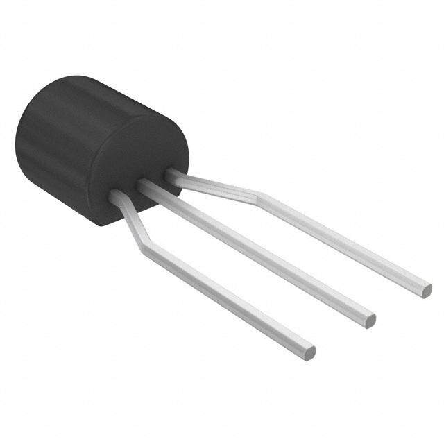
| 产品图片 |
|
| rohs | 否不符合限制有害物质指令(RoHS)规范要求 |
| 产品系列 | 电源管理 IC,参考电压,Analog Devices AD584JH- |
| 数据手册 | |
| 产品型号 | AD584JH |
| 串联VREF—电源电流—最大值 | 1 mA |
| 串联VREF—输入电压—最大值 | 30 V |
| 串联VREF—输入电压—最小值 | 4.5 V |
| 产品目录页面 | |
| 产品种类 | 参考电压 |
| 供应商器件封装 | TO-99-8 |
| 分流电流—最大值 | 10 mA |
| 初始准确度 | 0.3 % |
| 包装 | 散装 |
| 参考类型 | Series Precision References |
| 商标 | Analog Devices |
| 安装类型 | 通孔 |
| 安装风格 | Through Hole |
| 容差 | ±0.3% |
| 封装 | Bulk |
| 封装/外壳 | TO-99-8 金属罐 |
| 封装/箱体 | TO-99-8 |
| 工作温度 | 0°C ~ 70°C |
| 工厂包装数量 | 100 |
| 平均温度系数—典型值 | 30 PPM / C |
| 最大工作温度 | + 70 C |
| 最小工作温度 | 0 C |
| 标准包装 | 1 |
| 温度系数 | 30ppm/°C |
| 电压-输入 | 4.5 V ~ 30 V |
| 电压-输出 | 2.5V,5V,7.5V,10V |
| 电流-输出 | 10mA |
| 电流-阴极 | - |
| 电流-静态 | 1mA |
| 电源电流 | 0.75 mA |
| 系列 | AD584 |
| 输入电压 | 4.5 V to 30 V |
| 输出电压 | 2.5 V, 5 V, 7.5 V, 10 V |
| 通道数 | 1 |






- 商务部:美国ITC正式对集成电路等产品启动337调查
- 曝三星4nm工艺存在良率问题 高通将骁龙8 Gen1或转产台积电
- 太阳诱电将投资9.5亿元在常州建新厂生产MLCC 预计2023年完工
- 英特尔发布欧洲新工厂建设计划 深化IDM 2.0 战略
- 台积电先进制程称霸业界 有大客户加持明年业绩稳了
- 达到5530亿美元!SIA预计今年全球半导体销售额将创下新高
- 英特尔拟将自动驾驶子公司Mobileye上市 估值或超500亿美元
- 三星加码芯片和SET,合并消费电子和移动部门,撤换高东真等 CEO
- 三星电子宣布重大人事变动 还合并消费电子和移动部门
- 海关总署:前11个月进口集成电路产品价值2.52万亿元 增长14.8%



PDF Datasheet 数据手册内容提取
Pin Programmable, Precision Voltage Reference Data Sheet AD584 FEATURES PIN CONFIGURATIONS Four programmable output voltages TAB 10.000 V, 7.500 V, 5.000 V, and 2.500 V 8 10.0V 1 V+ 7 CAP Laser-trimmed to high accuracies AD584 No external components required 5.0V 2 TOP VIEW 6 VBG (Not to Scale) Trimmed temperature coefficient 1155 ppppmm//°°CC mmaaxxiimmuumm,, 0−°5C5 t°Co 7to0 °+C1 (2A5D°C5 8(A4DK)5 84T) 2.5V 3 COM4MON 5 STROBE 00527-001 Zero output strobe terminal provided Figure 1. 8-Pin TO-99 2-terminal negative reference: capability (5 V and above) 10.0V 1 8 V+ Output sources or sinks current 5.0V 2 AD584 7 CAP L1o0w m qAu cieusrrceenntt ocuurtrpeuntt c: a1p.0a mbiAlit my aximum COMM2.O5NV 34 (NToOt Pto V SIEcaWle) 56 VSBTGROBE 00527-002 MIL-STD-883 compliant versions available Figure 2. 8-Lead PDIP GENERAL DESCRIPTION The AD584 is an 8-terminal precision voltage reference offering The AD584J and AD584K are specified for operation from 0°C pin programmable selection of four popular output voltages: to +70°C, and the AD584S and AD584T are specified for the 10.000 V, 7.500 V, 5.000 V and 2.500 V. Other output voltages, −55°C to +125°C range. All grades are packaged in a hermetically above, below, or between the four standard outputs, are available by sealed, eight-terminal TO-99 metal can, and the AD584J and the addition of external resistors. The input voltage can vary AD584K are also available in an 8-lead PDIP. between 4.5 V and 30 V. PRODUCT HIGHLIGHTS Laser wafer trimming (LWT) is used to adjust the pin 1. The flexibility of the AD584 eliminates the need to design- programmable output levels and temperature coefficients, in and inventory several different voltage references. resulting in the most flexible high precision voltage reference Furthermore, one AD584 can serve as several references available in monolithic form. simultaneously when buffered properly. In addition to the programmable output voltages, the AD584 2. Laser trimming of both initial accuracy and temperature offers a unique strobe terminal that permits the device to be coefficient results in very low errors overtemperature turned on or off. When the AD584 is used as a power supply without the use of external components. reference, the supply can be switched off with a single, low power 3. The AD584 can be operated in a 2-terminal Zener mode at signal. In the off state, the current drained by the AD584 is reduced a 5 V output and above. By connecting the input and the to approximately 100 µA. In the on state, the total supply current is output, the AD584 can be used in this Zener configuration typically 750 µA, including the output buffer amplifier. as a negative reference. 4. The output of the AD584 is configured to sink or source The AD584 is recommended for use as a reference for 8-, 10-, currents. This means that small reverse currents can be or 12-bit digital-to-analog converters (DACs) that require an tolerated in circuits using the AD584 without damage to external precision reference. In addition, the device is ideal for the reference and without disturbing the output voltage analog-to-digital converters (ADCs) of up to 14-bit accuracy, (10 V, 7.5 V, and 5 V outputs). either successive approximation or integrating designs, and in 5. The AD584 is available in versions compliant with MIL-STD- general, it can offer better performance than that provided by 883. Refer to the Analog Devices current AD584/883B data standard self-contained references. sheet for detailed specifications. This can be found under the Additional Data Sheets section of the AD584 product page. Rev. C Information furnished by Analog Devices is believed to be accurate and reliable. However, no responsibility is assumed by Analog Devices for its use, nor for any infringements of patents or other One Technology Way, P.O. Box 9106, Norwood, MA 02062-9106, U.S.A. rights of third parties that may result from its use. Specifications subject to change without notice. No license is granted by implication or otherwise under any patent or patent rights of Analog Devices. Tel: 781.329.4700 www.analog.com Trademarks and registered trademarks are the property of their respective owners. Fax: 781.461.3113 ©1978–2012 Analog Devices, Inc. All rights reserved.
AD584 Data Sheet TABLE OF CONTENTS Features .............................................................................................. 1 Output Current Characteristics ...................................................7 Pin Configurations ........................................................................... 1 Dynamic Performance ..................................................................7 General Description ......................................................................... 1 Noise Filtering ...............................................................................8 Product Highlights ........................................................................... 1 Using the Strobe Terminal ...........................................................8 Revision History ............................................................................... 2 Percision High Current Supply....................................................8 Specifications ..................................................................................... 3 The AD584 as a Current Limiter.................................................9 Absolute Maximum Ratings ............................................................ 5 Negative Reference Voltages from an AD584 ...............................9 ESD Caution .................................................................................. 5 10 V Reference with Multiplying CMOS DACs or ADCs .......9 Theory of Operation ........................................................................ 6 Precision DAC Reference .......................................................... 10 Applying the AD584 .................................................................... 6 Outline Dimensions ....................................................................... 11 Performance over Temperature .................................................. 7 Ordering Guide .......................................................................... 12 REVISION HISTORY 5/12—Rev. B to Rev. C Deleted AD584L ................................................................. Universal Changes to Features Section, General Description Section and Product Highlights Section ............................................................. 1 Deleted Metalization Photograph .................................................. 4 Changes to 10 V Reference with Multiplying CMOS DACs or ADCs Section .................................................................................... 9 Changes to Precision DAC Reference Section and Figure 19... 10 Updated Outline Dimensions ....................................................... 11 Changes to Ordering Guide .......................................................... 12 7/01—Rev. A to Rev. B Rev. C | Page 2 of 12
Data Sheet AD584 SPECIFICATIONS V = 15 V and 25°C, unless otherwise noted. IN Specifications shown in boldface are tested on all production units at final electrical test. Results from those tests are used to calculate outgoing quality levels. All minimum and maximum specifications are guaranteed; although, only those shown in boldface are tested on all production units. Table 1. AD584J AD584K Model Min Typ Max Min Typ Max Unit OUTPUT VOLTAGE TOLERANCE Maximum Error at Pin 1 for Nominal Outputs of 10.000 V ±30 ±10 mV 7.500 V ±20 ±8 mV 5.000 V ±15 ±6 mV 2.500 V ±7.5 ±3.5 mV OUTPUT VOLTAGE CHANGE Maximum Deviation from 25°C Value, T to T 1 MIN MAX 10.000 V, 7.500 V, and 5.000 V Outputs 30 15 ppm/°C 2.500 V Output 30 15 ppm/°C Differential Temperature Coefficients Between Outputs 5 3 ppm/°C QUIESCENT CURRENT 0.75 1.0 0.75 1.0 mA Temperature Variation 1.5 1.5 µA/°C TURN-ON SETTLING TIME TO 0.1% 200 200 µs NOISE (0.1 Hz TO 10 Hz) 50 50 µV p-p LONG-TERM STABILITY 25 25 ppm/1000 Hrs SHORT-CIRCUIT CURRENT 30 30 mA LINE REGULATION (NO LOAD) 15 V ≤ VIN ≤ 30 V 0.002 0.002 %/V (VOUT + 2.5 V) ≤ VIN ≤ 15 V 0.005 0.005 %/V LOAD REGULATION 0 ≤ IOUT ≤ 5 mA, All Outputs 20 50 20 50 ppm/mA OUTPUT CURRENT VIN ≥ VOUT + 2.5 V Source at 25°C 10 10 mA Source TMIN to TMAX 5 5 mA Sink TMIN to TMAX 5 5 mA TEMPERATURE RANGE Operating 0 70 0 70 °C Storage −65 +175 −65 +175 °C PACKAGE OPTION 8-Pin Metal Header (TO-99, H-08) AD584JH AD584KH 8-Lead Plastic Dual In-Line Package (PDIP, N-8) AD584JN AD584KN 1 Calculated as average over the operating temperature range. Rev. C | Page 3 of 12
AD584 Data Sheet Specifications shown in boldface are tested on all production units at final electrical test. Results from those tests are used to calculate outgoing quality levels. All minimum and maximum specifications are guaranteed; although, only those shown in boldface are tested on all production units. Table 2. AD584S AD584T Model Min Typ Max Min Typ Max Unit OUTPUT VOLTAGE TOLERANCE Maximum Error at Pin 1 for Nominal Outputs of 10.000 V ±30 ±10 mV 7.500 V ±20 ±8 mV 5.000 V ±15 ±6 mV 2.500 V ±7.5 ±3.5 mV OUTPUT VOLTAGE CHANGE Maximum Deviation from 25°C Value, T to T 1 MIN MAX 10.000 V, 7.500 V, and 5.000 V Outputs 30 15 ppm/°C 2.500 V Output 30 20 ppm/°C Differential Temperature Coefficients Between Outputs 5 3 ppm/°C QUIESCENT CURRENT 0.75 1.0 0.75 1.0 mA Temperature Variation 1.5 1.5 µA/°C TURN-ON SETTLING TIME TO 0.1% 200 200 µs NOISE (0.1 Hz TO 10 Hz) 50 50 µV p-p LONG-TERM STABILITY 25 25 ppm/1000 Hrs SHORT-CIRCUIT CURRENT 30 30 mA LINE REGULATION (NO LOAD) 15 V ≤ VIN ≤ 30 V 0.002 0.002 %/V (VOUT + 2.5 V) ≤ VIN ≤ 15 V 0.005 0.005 %/V LOAD REGULATION 0 ≤ IOUT ≤ 5 mA, All Outputs 20 50 20 50 ppm/mA OUTPUT CURRENT V ≥ V + 2.5 V IN OUT Source at 25°C 10 10 mA Source T to T 5 5 mA MIN MAX Sink T to T 5 5 mA MIN MAX TEMPERATURE RANGE Operating −55 +125 −55 +125 °C Storage −65 +175 −65 +175 °C PACKAGE OPTION 8-Pin Metal Header (TO-99, H-08) AD584SH AD584TH 1 Calculated as average over the operating temperature range. Rev. C | Page 4 of 12
Data Sheet AD584 ABSOLUTE MAXIMUM RATINGS ESD CAUTION Table 3. Parameter Rating Input Voltage V to Ground 40 V IN Power Dissipation at 25°C 600 mW Operating Junction Temperature Range −55°C to +125°C Lead Temperature (Soldering 10 sec) 300°C Thermal Resistance Junction-to-Ambient (H-08A) 150°C/W Stresses above those listed under Absolute Maximum Ratings may cause permanent damage to the device. This is a stress rating only; functional operation of the device at these or any other conditions above those indicated in the operational section of this specification is not implied. Exposure to absolute maximum rating conditions for extended periods may affect device reliability. Rev. C | Page 5 of 12
AD584 Data Sheet THEORY OF OPERATION APPLYING THE AD584 approximately 20 V, even for the large values of R1. Do not omit R2; choose its value to limit the output to a value that can With power applied to Pin 8 and Pin 4 and all other pins open, be tolerated by the load circuits. If R2 is zero, adjusting R1 to its the AD584 produces a buffered nominal 10.0 V output between lower limit results in a loss of control over the output voltage. Pin 1 and Pin 4 (see Figure 3). The stabilized output voltage can When precision voltages are set at levels other than the standard be reduced to 7.5 V, 5.0 V, or 2.5 V by connecting the programming outputs, account for the 20% absolute tolerance in the internal pins as shown in Table 4. resistor ladder. Table 4. Alternatively, the output voltage can be raised by loading the Output 2.5 V tap with R3 alone. The output voltage can be lowered by Voltage (V) Pin Programming connecting R4 alone. Either of these resistors can be a fixed 7.5 Join the 2.5 V (Pin 3) and 5.0 V (Pin 2) pins. resistor selected by test or an adjustable resistor. In all cases, the 5.0 Connect the 5.0 V pin (Pin 2) to the output pin (Pin 1). resistors should have a low temperature coefficient to match the 2.5 Connect the 2.5 V pin (Pin 3) to the output pin (Pin 1). AD584 internal resistors, which have a negative temperature The options shown in Table 4 are available without the use of any coefficient less than 60 ppm/°C. If both R3 and R4 are used, additional components. Multiple outputs using only one AD584 these resistors should have matching temperature coefficients. can be provided by buffering each voltage programming pin When only small adjustments or trims are required, the circuit with a unity-gain, noninverting op amp. in Figure 4 offers better resolution over a limited trim range. The VSUPPLY circuit can be programmed to 5.0 V, 7.5 V, or 10 V, and it can be 8 adjusted by means of R1 over a range of about ±200 mV. To trim AD584 VOUT the 2.5 V output option, R2 (see Figure 4) can be reconnected to 10V the band gap reference (Pin 6). In this configuration, limit the 1 1.215V 24kΩ adjustment to ±100 mV to avoid affecting the performance of R4 5V the AD584. * 2 12kΩ V+ 2.5V R1 3 8 VOUT 6kΩ 10.0V VBG R3 1 6 R2 2 5.0V 6kΩ R2 AD584 2.5V 300kΩ R1 3 10kΩ COMMON 4 6 VBG *TAINHN AED N 2SY.H5 TVOR UTIALMFDP Ci gNIOSuO NUrTFeS IB3GEE.DU V CRIaNHArTATiaEINObRGNlNeE.A DOL uLBYtYp AMuStO OAR pEB tITiAoHSnA sPN O 1I0N0TmV 00527-004 4 COMMON 00527-005 Figure 4. Output Trimming The AD584 can also be programmed over a wide range of output V+ voltages, including voltages greater than 10 V, by the addition R40 R41 Q7 STROBE of one or more external resistors. Figure 3 illustrates the general Q20 Q10 Q11 Q8 adjustment procedure, with approximate values given for the C52 Q12 Q15 R42 internal resistors of the AD584. The AD584 may be modeled OUT 10V as an op amp with a noninverting feedback connection, driven C51 Q6 Q14 R34 5V TAP R37 by a high stability 1.215 V band gap reference (see Figure 5 for Q5 2.5V TAP schematic). Q16 Q13 R35 SUB When the feedback ratio is adjusted with external resistors, the C50 R33 R32 output amplifier can be made to multiply the reference voltage CAP by almost any convenient amount, making popular outputs of Q3 Q4 10.24 V, 5.12 V, 2.56 V, or 6.3 V easy to obtain. The most general R38 Q2 VBG adjustment (which gives the greatest range and poorest resolution) Q1 R30 uses R1 and R2 alone (see Figure 3). As R1 is adjusted to its upper limit, the 2.5V pin (Pin 3) is connected to the output, which R39 R31 R36 V– 00527-006 reduces to 2.5 V. As R1 is adjusted to its lower limit, the output Figure 5. Schematic Diagram voltage rises to a value limited by R2. For example, if R2 is approximately 6 kΩ, the upper limit of the output range is Rev. C | Page 6 of 12
Data Sheet AD584 PERFORMANCE OVER TEMPERATURE supply or ground. Figure 7 shows the output voltage vs. the output current characteristics of the device. Source current is Each AD584 is tested at three temperatures over the −55°C to displayed as negative current in the figure, and sink current is +125°C range to ensure that each device falls within the maximum displayed as positive current. The short-circuit current (that is, error band (see Figure 6) specified for a particular grade (that is, S 0 V output) is about 28 mA; however, when shorted to 15 V, the and T grades); three-point measurement guarantees performance sink current goes to approximately 20 mA. within the error band from 0°C to 70°C (that is, J and K grades). The error band guaranteed for the AD584 is the maximum +VS = 15V deviation from the initial value at 25°C. Thus, given the grade 14 TA = 25°C of the AD584, the maximum total error from the initial tolerance 12 plus the temperature variation can easily be determined. For V) example, for the AD584T, the initial tolerance is ±10 mV, and GE (10 A the error band is ±15 mV. Therefore, the unit is guaranteed to T L O 8 be 10.000 V ± 25 mV from −55°C to +125°C. V T U 10.005 TP 6 U O 4 2 0 V (V)OUT10.000 –20 –S1O5URC–1EO0UTP–U5T CU0RREN5T (mA1)0SINK15 20 00527-008 Figure 7. Output Voltage vs. Output Current (Sink and Source) DYNAMIC PERFORMANCE Many low power instrument manufacturers are becoming increasingly concerned with the turn-on characteristics of the 9.995–55 0 TEMP2E5RATURE (°C)70 125 00527-007 ocoftmenp oenneanbtlse btheien gen uds euds ienr tthoe kire seyps tpeomwse. rF aosftf twurhne-no nn octo mnepeodneedn ts Figure 6. Typical Temperature Characteristic and yet respond quickly when the power is turned on. Figure 8 displays the turn-on characteristic of the AD584. Figure 8 is OUTPUT CURRENT CHARACTERISTICS generated from cold-start operation and represents the true The AD584 has the capability to either source or sink current turn-on waveform after an extended period with the supplies off. and provide good load regulation in either direction; although, Figure 8 shows both the coarse and fine transient characteristics of it has better characteristics in the source mode (positive current the device; the total settling time to within ±10 mV is about into the load). The circuit is protected for shorts to either positive 180 µs, and there is no long thermal tail appearing after the point. 12V 10.03V OUTPUT 11V 10.02V OUTPUT 10.01V 10V 10.00V 20V POWER SUPPLY 10V INPUT 0V 0 SE5T0TLIN1G0 0TIM1E5 (0µs)200 250 00527-009 Figure 8. Output Settling Characteristic Rev. C | Page 7 of 12
AD584 Data Sheet NOISE FILTERING USING THE STROBE TERMINAL The bandwidth of the output amplifier in the AD584 can be The AD584 has a strobe input that can be used to zero the output. reduced to filter output noise. A capacitor ranging between 0.01 µF This unique feature permits a variety of new applications in and 0.1 µF connected between the CAP and V terminals further signal and power conditioning circuits. BG reduces the wideband and feedthrough noise in the output of Figure 11 illustrates the strobe connection. A simple NPN switch the AD584, as shown in Figure 9 and Figure 10. However, this can be used to translate a TTL logic signal into a strobe of the tends to increase the turn-on settling time of the device; therefore, output. The AD584 operates normally when there is no current allow for ample warm-up time. drawn from Pin 5. Bringing this terminal low, to less than 200 mV, SUPPLY allows the output voltage to go to zero. In this mode, the AD584 V+ is not required to source or sink current (unless a 0.7 V residual 8 CAP output is permissible). If the AD584 is required to sink a transient 7 1 10.0V 0.01µF* current while strobe is off, limit the strobe terminal input current TO AD584 0.1µF by a 100 Ω resistor, as shown in Figure 11. VBG 6 4 V+ 8 STROBE 10.0V *INCREASES TURN-ONC OTIMMMEON 00527-010 100Ω 5 AD584 12 Figure 9. Additional Noise Filtering with an External Capacitor 3 1000 NOISE SPECTRAL DENSITY (nV1/0 0 HpzF) LINOPGUICT HLOI = = O OFNF 201k0ΩkΩ 2N2222 4 COMMON 00527-012 NO CAP Figure 11. Use of the Strobe Terminal 1000pF 100 The strobe terminal tolerates up to 5 µA leakage, and its driver 0.01µF should be capable of sinking 500 µA continuous. A low leakage, open collector gate can be used to drive the strobe terminal directly, provided the gate can withstand the AD584 output voltage plus 1 V. NO CAP TOTAL NOISE (µV rms) UP TO 10 SPECIFIED FREQUENCY PERCISION HIGH CURRENT SUPPLY The AD584 can be easily connected to a power PNP or power PNP Darlington device to provide much greater output current capability. The circuit shown in Figure 12 delivers a precision 110 100 FR1kEQUENCY 1(H0kz) 100k 1M 00527-011 1si0g nVif iocuatnptu cta pwaicthit iuvep ctoom 4p Ao nseunptp, ltiheed 0 t.o1 tµhFe c laopaadc.i tIof rt hise r eloqaudir heda.s a Figure 10. Spectral Noise Density and Total RMS Noise vs. Frequency If the load is purely resistive, improved high frequency, supply rejection results from removing the capacitor. VIN ≥ 15V 470Ω 2N6040 0.1µF V+ 8 AD584 110.0V VOUT 10V @ 4A 4 COMMON 00527-013 Figure 12. High Current Precision Supply Rev. C | Page 8 of 12
Data Sheet AD584 The AD584 can also use an NPN or NPN Darlington transistor to The temperature characteristics and long-term stability of the boost its output current. Simply connect the 10 V output terminal device is essentially the same as that of a unit used in standard of the AD584 to the base of the NPN booster and take the 3-terminal mode. output from the booster emitter, as shown in Figure 13. The ANALOG GND 5.0V pin or the 2.5V pin must connect to the actual output in V+ 8 this configuration. Variable or adjustable outputs (as shown in VOUT 1µF 1 Figure 3 and Figure 4) can be combined with a 5.0 V connection to AD584 2 obtain outputs above 5.0 V. 5.0V TAP RAW SUPPLY (≈5V > VOUT) 4 COMMON VREF DNAPNR L2INN6G0T5O7N RS –5V V+ –15V25.%4kΩ 00527-016 8 Figure 15. 2-Terminal, −5 V Reference 10.0V 1 5.0V VOUT The AD584 can also be used in 2-terminal mode to develop a AD584 2 (5V, 12A 2.5V AS SHOWN) positive reference. VIN and VOUT are tied together and to the 3 positive supply through an appropriate supply resistor. The 4 COMMON 1kΩ 00527-014 p2-etrefromrminaanl cceo cnhnaercatciotenr.i sTtihces oarnel ys iamdvilaanr ttaog teh oofs teh oisf aco nnengeactitvioen Figure 13. NPN Output Current Booster over the standard 3-terminal connection is that a lower primary THE AD584 AS A CURRENT LIMITER supply can be used, as low as 0.5 V above the desired output The AD584 represents an alternative to current limiter diodes voltage. This type of operation requires considerable attention that require factory selection to achieve a desired current. Use of to load and to the primary supply regulation to ensure that the current limiting diodes often results in temperature coefficients AD584 always remains within its regulating range of 1 mA to of 1%/°C. Use of the AD584 in this mode is not limited to a set 5 mA (2 mA to 5 mA for operation beyond 85°C). current limit; it can be programmed from 0.75 mA to 5 mA 10 V REFERENCE WITH MULTIPLYING CMOS DACs with the insertion of a single external resistor (see Figure 14). OR ADCs The minimum voltage required to drive the connection is 5 V. The AD584 is ideal for application with the AD7533 10-bit multiplying CMOS DAC, especially for low power applications. V+ 8 It is equally suitable for the AD7574 8-bit ADC. In the standard VOUT = 2.5V 1 hook-up, as shown in Figure 16, the standard output voltages are AD584 3 2.5V = i 2.5V+ 0.75mA inverted by the amplifier/DAC configuration to produce converted TAP R voltage ranges. For example, a +10 V reference produces a 0 V to 4 RLOAD −10 V range. If an OP1177 amplifier is used, total quiescent COMMON 00527-015 supply current is typically 2 mA+1.5 V Figure 14. A Two-Component Precision Current Limiter NEGATIVE REFERENCE VOLTAGES FROM AN AD584 V+ 8 10.0V The AD584 can also be used in a 2-terminal Zener mode to AD584 1 provide a precision −10 V, −7.5 V, or −5.0 V reference. As shown in 4 Figure 15, the VIN and VOUT terminals are connected together to COMMON the positive supply (in this case, ground). The AD584 COMMON VREF 15 14 pin is connected through a resistor to the negative supply. The BIT 1 (MSB) RFB DIGITAL 4 16 output is now taken from the COMMON pin instead of VOUT. With INPUT 5 +15V 1 mA flowing through the AD584 in this mode, a typical unit AD7533 1 IOUT1 shows a 2 mV increase in the output level over that produced in VOUT 13 2 IOUT2 0V TO –10V 3th-tise rcmoninnaelc mtioond ein. cArlesaos,e ns oftreo mth a0t. 2th Ωe etfyfpeicctaivl et oo u2 tΩpu. tI ti misp eesdsaennctiea iln BIT 10 (LSB) 3 C–O15MVMON 00527-017 to arrange the output load and the supply resistor, R, so that S Figure 16. Low Power 10-Bit CMOS DAC Application the net current through the AD584 is always between 1 mA and 5 mA (between 2 mA and 5 mA for operation beyond 85°C). Rev. C | Page 9 of 12
AD584 Data Sheet The AD584 is normally used in the −10 V mode with the AD7574 scale temperature coefficient of 18 ppm/°C more than the to give a 0 V to +10 V ADC range. This is shown in Figure 17. commercial range. The 10 V reference also supplies the normal Bipolar output applications and other operating details can be 1 mA bipolar offset current through the 9.95 kΩ bipolar offset found in the data sheets for the CMOS products. resistor. The bipolar offset temperature coefficient thus depends –15V +15V only on the temperature coefficient matching of the bipolar offset R3 resistor to the input reference resistor and is guaranteed to V+ 8 AD584 4 COMMON 15.%2kΩ GRA2IN 2 kTΩR*IM 12 (TAODP7 V5I7E4W) 18 3 ppm/°C. Figure 18 demonstrates the flexibility of the AD584 –10V REF DIGITAL applied to another popular digital-to-analog configuration. R1 3 SUPPLY 10.0V1 0.1µF SIIGNNPUATL2kΩ 10%* 4 RETURN V+ V+ 0V TO +10V 5 GROUND *RG1A IANN TDR RIM2 CISA NNO BTE R OEMQIUTITREEDD I.F GANRAOLUONGDINTERTIE 00527-019 A1 (MSAB2) 56 13 1145 VVRREEFF ((+–)) R14 10.0V 1 AD8584 Figure 17. AD584 as −10 V Reference for CMOS ADC AA34 78 AD R15 2.5V 3 DAC08 4 PRECISION DAC REFERENCE A5 9 R14 = R15 COMMON A6 10 RL The AD565A, like many DACs, can operate with an external A7 11 4 10 V reference element (see Figure 19). This 10 V reference A8 (LSB) 12 IO COMP 16 1 VLC voltage is converted into a reference current of approximately 3 2 C 01.050 m ΩA t rvimia mtheer i)n. Ttehrne agla 1in9. 9te5m kpΩe rraetsuisrteo cro (einff isceireinets owf itthhe t hAeD e5xt6e5rAna l V– IOUT 00527-020 is primarily governed by the temperature tracking of the 19.95 kΩ Figure 18. Current Output, 8-Bit Digital-to-Analog Configuration resistor and the 5 kΩ/10 kΩ span resistors; this gain temperature coefficient is guaranteed to 3 ppm/°C. Therefore, using the AD584K (at 5 ppm/°C) as the 10 V reference guarantees a maximum full- BIPOLAR OFFSET ADJUST 15T R1 +15V 100Ω 0.1µF REF OUT VCC BIPOLAR OFF +15V 20V SPAN 8 GAIN 10V AD565A 5kΩ ADJUST REF AD584 1 15T IN 19.95kΩ 0.5mA 9.95kΩ 10V SPAN +15V 4 10R02Ω GRNEDF 20kΩ IREF 4IO ×U TIR =EF ×D ACOCDE IO 5kΩ8kΩ DAC OUT 23 OP16177 OO±1PU0 TVAPMUPT CODE INPUT –15V –VEE POWGNEDR MSB LSB 0.1µ–F15V 00527-018 Figure 19. Precision 12-Bit DAC Rev. C | Page 10 of 12
Data Sheet AD584 OUTLINE DIMENSIONS REFERENCE PLANE 0.5000 (12.70) 0.1850 (4.70) MIN 0.1650 (4.19) 0.2500 (6.35) MIN 0.1000 (2.54) 0.0500 (1.27) MAX BSC 0.1600 (4.06) 0.1400 (3.56) 5 0.3700 (9.40)0.3350 (8.51) 0.3350 (8.51)0.3050 (7.75) 0(B.52.S00C080) 324 867 00..00425700 ((10..1649)) 0.0190 (0.48) 0.1000 1 (2.54) 0.0400 (1.02) MAX 0.0160 (0.41) BSC 0.0340 (0.86) 0.0210 (0.53) 0.0280 (0.71) 0.0400 (1.02) 0.0160 (0.41) 0.0100 (0.25) 45° BSC BASE & SEATING PLANE COMPLIANTTO JEDEC STANDARDS MO-002-AK C(RINOEFNPEATRRREOENNLCLTEIHN EOGSN EDLSIYM)AEANNRDSEI AORRNOESU NANORDEET DAIN-PO IPFNRFCO HINPECRSHI;A METEQIL UFLIOIVMRAE LUTEESNRET ISDN I FMDOEERSNISGINO.NS 022306-A Figure 20. 8-Pin Metal Header [TO-99] (H-08) Dimensions shown in inches and (millimeters) 0.400 (10.16) 0.365 (9.27) 0.355 (9.02) 8 5 0.280 (7.11) 0.250 (6.35) 1 4 0.240 (6.10) 0.325 (8.26) 0.310 (7.87) 0.100 (2.54) 0.300 (7.62) BSC 0.060 (1.52) 0.195 (4.95) 0.210 (5.33) MAX 0.130 (3.30) MAX 0.115 (2.92) 0.015 0.150 (3.81) (0.38) 0.015 (0.38) 0.130 (3.30) MIN GAUGE 0.115 (2.92) SEATING PLANE 0.014 (0.36) PLANE 0.010 (0.25) 0.022 (0.56) 0.008 (0.20) 0.005 (0.13) 0.430 (10.92) 0.018 (0.46) MIN MAX 0.014 (0.36) 0.070 (1.78) 0.060 (1.52) 0.045 (1.14) COMPLIANTTO JEDEC STANDARDS MS-001 CONTROLLING DIMENSIONSARE IN INCHES; MILLIMETER DIMENSIONS (RCINEOFRPEANRREERENN LCTEEHA EODSNSEL MSY)AAAYNR BDEE AR CROOEU NNNFODIGETUDAR-POEPFDRFOA INSPC RWHIAH ETOEQL UFEIO VORAR LU EHSNAETL ISFN FLDOEEARSDIGSN.. 070606-A Figure 21. 8-Lead Plastic Dual In-Line Package [PDIP] Narrow Body (N-8) Dimensions shown in inches and (millimeters) Rev. C | Page 11 of 12
AD584 Data Sheet ORDERING GUIDE Output Initial Accuracy Temperature Coefficient Temperature Package Package Ordering Model1 Voltage (V ) mV % (ppm/°C) Range (°C) Description Option Quantity O AD584JH 2.5 ±7.5 0.30 30 0 to 70 8-Pin TO-99 H-08 100 AD584JNZ 2.5 ±7.5 0.30 30 0 to 70 8-Lead PDIP N-8 50 AD584KH 2.5 ±3.5 0.14 15 0 to 70 8-Pin TO-99 H-08 100 AD584KNZ 2.5 ±3.5 0.14 15 0 to 70 8-Lead PDIP N-8 50 AD584SH 2.5 ±7.5 0.30 30 −55 to +125 8-Pin TO-99 H-08 100 AD584SH/883B 2.5 ±7.5 0.30 30 −55 to +125 8-Pin TO-99 H-08 100 AD584TH 2.5 ±3.5 0.14 20 −55 to +125 8-Pin TO-99 H-08 100 AD584TH/883B 2.5 ±3.5 0.14 20 −55 to +125 8-Pin TO-99 H-08 100 AD584JH 5.0 ±15.0 0.30 30 0 to 70 8-Pin TO-99 H-08 100 AD584JNZ 5.0 ±15.0 0.30 30 0 to 70 8-Lead PDIP N-8 50 AD584KH 5.0 ±6.0 0.12 15 0 to 70 8-Pin TO-99 H-08 100 AD584KNZ 5.0 ±6.0 0.12 15 0 to 70 8-Lead PDIP N-8 50 AD584SH 5.0 ±15.0 0.14 30 −55 to +125 8-Pin TO-99 H-08 100 AD584SH/883B 5.0 ±15.0 0.30 30 −55 to +125 8-Pin TO-99 H-08 100 AD584TH 5.0 ±6.0 0.30 15 −55 to +125 8-Pin TO-99 H-08 100 AD584TH/883B 5.0 ±6.0 0.12 15 −55 to +125 8-Pin TO-99 H-08 100 AD584JH 7.5 ±20.0 0.27 30 0 to 70 8-Pin TO-99 H-08 100 AD584JNZ 7.5 ±20.0 0.27 30 0 to 70 8-Lead PDIP N-8 50 AD584KH 7.5 ±8.0 0.11 15 0 to 70 8-Pin TO-99 H-08 100 AD584KNZ 7.5 ±8.0 0.11 15 0 to 70 8-Lead PDIP N-8 50 AD584SH 7.5 ±20.0 0.27 30 −55 to +125 8-Pin TO-99 H-08 100 AD584SH/883B 7.5 ±20.0 0.27 30 −55 to +125 8-Pin TO-99 H-08 100 AD584TH 7.5 ±8.0 0.11 15 −55 to +125 8-Pin TO-99 H-08 100 AD584TH/883B 7.5 ±8.0 0.11 15 −55 to +125 8-Pin TO-99 H-08 100 AD584JH 10.0 ±30.0 0.30 30 0 to 70 8-Pin TO-99 H-08 100 AD584JNZ 10.0 ±30.0 0.30 30 0 to 70 8-Lead PDIP N-8 50 AD584KH 10.0 ±10.0 0.10 15 0 to 70 8-Pin TO-99 H-08 100 AD584KNZ 10.0 ±10.0 0.10 15 0 to 70 8-Lead PDIP N-8 50 AD584SH 10.0 ±30.0 0.30 30 −55 to +125 8-Pin TO-99 H-08 100 AD584SH/883B 10.0 ±30.0 0.30 30 −55 to +125 8-Pin TO-99 H-08 100 AD584TH 10.0 ±10.0 0.10 15 −55 to +125 8-Pin TO-99 H-08 100 AD584TH/883B 10.0 ±10.0 0.10 15 −55 to +125 8-Pin TO-99 H-08 100 1 Z = RoHS Compliant Part. ©1978–2012 Analog Devices, Inc. All rights reserved. Trademarks and registered trademarks are the property of their respective owners. D00527-0-5/12(C) Rev. C | Page 12 of 12
Mouser Electronics Authorized Distributor Click to View Pricing, Inventory, Delivery & Lifecycle Information: A nalog Devices Inc.: JM38510/12801BGA AD584KH AD584KNZ AD584JH AD584TH/883B AD584SH AD584SH/883B AD584JNZ AD584TH AD584-000C AD584R000C

 Datasheet下载


