ICGOO在线商城 > 集成电路(IC) > 数据采集 - 数模转换器 > AD5735ACPZ

 Datasheet下载
- 型号: AD5735ACPZ
- 制造商: Analog
- 库位|库存: xxxx|xxxx
- 要求:
| 数量阶梯 | 香港交货 | 国内含税 |
| +xxxx | $xxxx | ¥xxxx |
查看当月历史价格
查看今年历史价格
AD5735ACPZ产品简介:
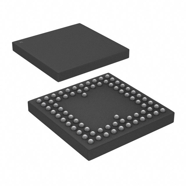
ICGOO电子元器件商城为您提供AD5735ACPZ由Analog设计生产,在icgoo商城现货销售,并且可以通过原厂、代理商等渠道进行代购。 AD5735ACPZ价格参考。AnalogAD5735ACPZ封装/规格:数据采集 - 数模转换器, 12 位 数模转换器 4 64-LFCSP-VQ(9x9)。您可以下载AD5735ACPZ参考资料、Datasheet数据手册功能说明书,资料中有AD5735ACPZ 详细功能的应用电路图电压和使用方法及教程。
| 参数 | 数值 |
| 产品目录 | 集成电路 (IC)半导体 |
| 描述 | IC DAC QUAD VOLT CUR 64-LFCSP数模转换器- DAC Quad Ch 12B Serial Inpt VOut |
| 产品分类 | |
| 品牌 | Analog Devices |
| 产品手册 | |
| 产品图片 |
|
| rohs | 符合RoHS无铅 / 符合限制有害物质指令(RoHS)规范要求 |
| 产品系列 | 数据转换器IC,数模转换器- DAC,Analog Devices AD5735ACPZ- |
| 数据手册 | |
| 产品型号 | AD5735ACPZ |
| 产品培训模块 | http://www.digikey.cn/PTM/IndividualPTM.page?site=cn&lang=zhs&ptm=26125http://www.digikey.cn/PTM/IndividualPTM.page?site=cn&lang=zhs&ptm=26140http://www.digikey.cn/PTM/IndividualPTM.page?site=cn&lang=zhs&ptm=26150http://www.digikey.cn/PTM/IndividualPTM.page?site=cn&lang=zhs&ptm=26147 |
| 产品种类 | 数模转换器- DAC |
| 位数 | 12 |
| 供应商器件封装 | 64-LFCSP-VQ(9x9) |
| 分辨率 | 12 bit |
| 包装 | 托盘 |
| 商标 | Analog Devices |
| 安装类型 | 表面贴装 |
| 安装风格 | SMD/SMT |
| 封装 | Tray |
| 封装/外壳 | 64-VFQFN 裸露焊盘,CSP |
| 封装/箱体 | LFCSP-64 |
| 工作温度 | -40°C ~ 105°C |
| 工厂包装数量 | 260 |
| 建立时间 | 18µs |
| 接口类型 | SPI |
| 数据接口 | DSP,MICROWIRE™,QSPI™,串行,SPI™ |
| 最大功率耗散 | 173 mW |
| 最大工作温度 | + 105 C |
| 最小工作温度 | - 40 C |
| 标准包装 | 1 |
| 电压参考 | Internal, External |
| 电压源 | 模拟和数字,双 ± |
| 电源电压-最大 | 5.5 V |
| 电源电压-最小 | 2.7 V |
| 积分非线性 | +/- 0.032 % FSR |
| 稳定时间 | 11 us |
| 系列 | AD5735 |
| 结构 | Segment |
| 转换器数 | 4 |
| 转换器数量 | 4 |
| 输出数和类型 | 4 电流,4 电压 |
| 输出类型 | Current, Voltage |
| 采样率(每秒) | * |


- 商务部:美国ITC正式对集成电路等产品启动337调查
- 曝三星4nm工艺存在良率问题 高通将骁龙8 Gen1或转产台积电
- 太阳诱电将投资9.5亿元在常州建新厂生产MLCC 预计2023年完工
- 英特尔发布欧洲新工厂建设计划 深化IDM 2.0 战略
- 台积电先进制程称霸业界 有大客户加持明年业绩稳了
- 达到5530亿美元!SIA预计今年全球半导体销售额将创下新高
- 英特尔拟将自动驾驶子公司Mobileye上市 估值或超500亿美元
- 三星加码芯片和SET,合并消费电子和移动部门,撤换高东真等 CEO
- 三星电子宣布重大人事变动 还合并消费电子和移动部门
- 海关总署:前11个月进口集成电路产品价值2.52万亿元 增长14.8%


PDF Datasheet 数据手册内容提取
Quad-Channel, 12-Bit, Serial Input, 4 mA to 20 mA and Voltage Output DAC with Dynamic Power Control Data Sheet AD5735 FEATURES On-chip dynamic power control minimizes package power dissipation in current mode. This reduced power dissipation 12-bit resolution and monotonicity is achieved by regulating the voltage on the output driver from Dynamic power control for thermal management 7.4 V to 29.5 V using a dc-to-dc boost converter optimized for Current and voltage output pins connectable to a single minimum on-chip power dissipation. terminal Current output ranges: 0 mA to 20 mA, 4 mA to 20 mA, The AD5735 uses a versatile 3-wire serial interface that operates and 0 mA to 24 mA at clock rates of up to 30 MHz and is compatible with standard ±0.1% total unadjusted error (TUE) maximum SPI, QSPI™, MICROWIRE®, DSP, and microcontroller interface Voltage output ranges (with 20% overrange): 0 V to 5 V, standards. The serial interface also features optional CRC-8 packet 0 V to 10 V, ±5 V, and ±10 V error checking, as well as a watchdog timer that monitors activity ±0.09% total unadjusted error (TUE) maximum on the interface. User-programmable offset and gain PRODUCT HIGHLIGHTS On-chip diagnostics On-chip reference: ±10 ppm/°C maximum 1. Dynamic power control for thermal management. −40°C to +105°C temperature range 2. 12-bit performance. 3. Quad channel. APPLICATIONS COMPANION PRODUCTS Process control Actuator control Product Family: AD5755, AD5755-1, AD5757, AD5737 PLCs External References: ADR445, ADR02 Digital Isolators: ADuM1410, ADuM1411 GENERAL DESCRIPTION Power: ADP2302, ADP2303 The AD5735 is a quad-channel voltage and current output DAC Additional companion products on the AD5735 product page that operates with a power supply range from −26.4 V to +33 V. FUNCTIONAL BLOCK DIAGRAM AVCC 5.0V AVSS AVDD –15V AGND +15V SWx VBOOST_x DVDD 7.4V TO 29.5V DGND LDAC DC-TO-DC CONVERTER SCLK SDIN SYNC INDTIEGRITFAALCE IOUT_x SDO + DAC A RSET_x CLEAR CURRENT AND VOLTAGE FAULT OUTPUT RANGE ALERT GAIN REG A SCALING +VSENSE_x AD1 OFFSET REG A VOUT_x AD0 DAC CHANNEL A –VSENSE_x REFOUT REFERENCE REFIN DAC CHANNEL B DAC CHANNEL C AD5735 DAC CHANNEL D N1.O xT =E SA, B, C, OR D. 09961-100 Figure 1. Rev. E Document Feedback Information furnished by Analog Devices is believed to be accurate and reliable. However, no responsibility is assumed by Analog Devices for its use, nor for any infringements of patents or other One Technology Way, P.O. Box 9106, Norwood, MA 02062-9106, U.S.A. rights of third parties that may result from its use. Specifications subject to change without notice. No license is granted by implication or otherwise under any patent or patent rights of Analog Devices. Tel: 781.329.4700 ©2011–2017 Analog Devices, Inc. All rights reserved. Trademarks and registered trademarks are the property of their respective owners. Technical Support www.analog.com
AD5735 Data Sheet TABLE OF CONTENTS Features .............................................................................................. 1 Data Registers ............................................................................. 33 Applications ....................................................................................... 1 Control Registers ........................................................................ 35 General Description ......................................................................... 1 Readback Operation .................................................................. 38 Product Highlights ........................................................................... 1 Device Features ............................................................................... 40 Companion Products ....................................................................... 1 Fault Output ................................................................................ 40 Functional Block Diagram .............................................................. 1 Voltage Output Short-Circuit Protection ................................ 40 Revision History ............................................................................... 3 Digital Offset and Gain Control ............................................... 40 Detailed Functional Block Diagram .............................................. 4 Status Readback During a Write .............................................. 40 Specifications ..................................................................................... 5 Asynchronous Clear ................................................................... 41 AC Performance Characteristics ................................................ 8 Packet Error Checking ............................................................... 41 Timing Characteristics ................................................................ 9 Watchdog Timer ......................................................................... 41 Absolute Maximum Ratings .......................................................... 12 Alert Output ................................................................................ 41 Thermal Resistance .................................................................... 12 Internal Reference ...................................................................... 41 ESD Caution ................................................................................ 12 External Current Setting Resistor ............................................ 42 Pin Configuration and Function Descriptions ........................... 13 Digital Slew Rate Control .......................................................... 42 Typical Performance Characteristics ........................................... 16 Dynamic Power Control............................................................ 43 Voltage Outputs .......................................................................... 16 DC-to-DC Converters ............................................................... 43 Current Outputs ......................................................................... 20 AI Supply Requirements—Static .......................................... 44 CC DC-to-DC Converter ................................................................. 24 AI Supply Requirements—Slewing ...................................... 44 CC Reference ..................................................................................... 25 Applications Information .............................................................. 46 General ......................................................................................... 26 Voltage and Current Output Pins on the Same Terminal ..... 46 Terminology .................................................................................... 27 Current Output Mode with Internal R ................................ 46 SET Theory of Operation ...................................................................... 29 Precision Voltage Reference Selection ..................................... 46 DAC Architecture ....................................................................... 29 Driving Inductive Loads ............................................................ 47 Power-On State of the AD5735 ................................................ 30 Transient Voltage Protection .................................................... 47 Serial Interface ............................................................................ 30 Microprocessor Interfacing ....................................................... 47 Transfer Function ....................................................................... 30 Layout Guidelines....................................................................... 47 Registers ........................................................................................... 31 Galvanically Isolated Interface ................................................. 48 Enabling the Output ................................................................... 32 Outline Dimensions ....................................................................... 49 Reprogramming the Output Range ......................................... 32 Ordering Guide .......................................................................... 49 Rev. E | Page 2 of 49
Data Sheet AD5735 REVISION HISTORY 6/2017—Rev. D to Rev. E 11/2012—Rev. B to Rev. C Changes to Figure 4......................................................................... 10 Changed Thermal Impedance from 20 °C/W to 28°C/W ......... 11 Changes to Figure 5......................................................................... 11 Changes to Pin 6 Description ........................................................ 12 Changes to Readback Operation Section ..................................... 38 Changes to Figure 25 ...................................................................... 17 Deleted Table 31 and Table 32; Renumbered Sequentially ........ 38 Changes to DUT_AD1, DUT_AD0 Description, Table 12 ....... 32 Changes to Asynchronous Clear Section ..................................... 41 Changes to Packet Error Checking Section and Internal Updated Outline Dimensions ........................................................ 49 Reference Section ............................................................................ 40 Changes to Figure 78 ...................................................................... 42 5/2014—Rev. C to Rev. D Changes to Figure 83 ...................................................................... 46 Changes to Thermal Hysteresis Parameter, Table 1 ...................... 6 Updated Outline Dimensions........................................................ 48 Changes to Table 3 ............................................................................ 9 Changes to Figure 4......................................................................... 10 5/2012—Rev. A to Rev. B Added Figure 5; Renumbered Sequentially and Changes to Changes to Figure 2 .......................................................................... 3 Figure 6 ............................................................................................. 11 Changes to Figure 54 to Figure 57 ................................................ 24 11/2011—Rev. 0 to Rev. A Changes to Voltage Reference Thermal Hysteresis Definition ..... 27 Added Comments to OUTPUT CHARACTERISTICS and Changes to Readback Operation Section ..................................... 38 ACCURACY, CURRENT OUTPUT Parameters in Added Table 31 and Table 32; Renumbered Sequentially .......... 38 Table 1 ................................................................................................. 4 Changes to Status Readback During a Write Section ................. 41 Changes to Power-On State of the AD5735 Section .................. 29 Changes to Packet Error Checking Section ................................. 42 Changes to Readback Operation Section..................................... 37 Changes to Table 38 ........................................................................ 43 7/2011—Revision 0: Initial Version Rev. E | Page 3 of 49
AD5735 Data Sheet DETAILED FUNCTIONAL BLOCK DIAGRAM AVCC 5.0V AVSS AVDD –15V AGND +15V SWA VBOOST_A DVDD POWER-ON DC-TO-DC DGND RESET CONVERTER LDAC DPYONWAMERIC 7.4VTO29.5V VSEN1 VSEN2 CONTROL CLEAR INPUT SHIFT SCLK REGISTER 12 DAC DAC 12 R2 R3 SDIN AND DATA + INPUT DACA SYNC CONTROL REGA REGA SDO FAULT GAINREGA IOUT_A OFFSETREGA STATUS REGISTER ALERT WATCHDOG R1 RSET_A TIMER (SPIACTIVITY) 30kΩ +VSENSE_A REFOUT VREF VOUT RANGE VOUT_A REFIN REBFUEFRFEENRCSE DACCHANNELA SCALING –VSENSE_A IOUT_B,IOUT_C,IOUT_D DACCHANNELB RSET_B,RSET_C,RSET_D AD1 AD5735 DACCHANNELC AD0 DACCHANNELD ±VSENSE_B,±VSENSE_C,±VSENSE_D SWB,SWC,SWD VBOOST_B,VBOOST_C,VBOOST_D VOUT_B,VOUT_C,VOUT_D 09961-001 Figure 2. Rev. E | Page 4 of 49
Data Sheet AD5735 SPECIFICATIONS AV = V = 15 V; AV = −15 V; DV = 2.7 V to 5.5 V; AV = 4.5 V to 5.5 V; dc-to-dc converter disabled; AGND = DGND = DD BOOST_x SS DD CC GNDSW = 0 V; REFIN = 5 V; voltage outputs: R = 1 kΩ, C = 220 pF; current outputs: R = 300 Ω; all specifications T to T , x L L L MIN MAX unless otherwise noted. Table 1. Parameter1 Min Typ Max Unit Test Conditions/Comments VOLTAGE OUTPUT Output Voltage Ranges 0 5 V 0 10 V −5 +5 V −10 +10 V 0 6 V 0 12 V −6 +6 V −12 +12 V Resolution 12 Bits ACCURACY, VOLTAGE OUTPUT Total Unadjusted Error (TUE) −0.09 ±0.012 +0.09 % FSR 0 V to 5 V, 0 V to 10 V, ±5 V, ±10 V ranges −0.13 ±0.05 +0.13 % FSR On overranges (0 V to 6 V, 0 V to 12 V, ±6 V, ±12 V) TUE Long-Term Stability 35 ppm FSR Drift after 1000 hours, T = 150°C J Relative Accuracy (INL) −0.032 ±0.006 +0.032 % FSR Differential Nonlinearity (DNL) −1 +1 LSB Guaranteed monotonic Zero-Scale Error −0.05 ±0.004 +0.05 % FSR 0 V to 5 V, 0 V to 10 V ranges −0.08 ±0.004 +0.08 % FSR On overranges (0 V to 6 V, 0 V to 12 V) Zero-Scale TC2 ±2 ppm FSR/°C Bipolar Zero Error −0.05 ±0.003 +0.05 % FSR ±5 V, ±10 V ranges −0.08 ±0.03 +0.08 % FSR On overranges (±6 V, ±12 V) Bipolar Zero TC2 ±2 ppm FSR/°C Offset Error −0.065 ±0.005 +0.065 % FSR 0 V to 5 V, 0 V to 10 V, ±5 V, ±10 V ranges −0.09 ±0.03 +0.09 % FSR On overranges (0 V to 6 V, 0 V to 12 V, ±6 V, ±12 V) Offset TC2 ±2 ppm FSR/°C Gain Error −0.08 ±0.004 +0.08 % FSR 0 V to 5 V, 0 V to 10 V, ±5 V, ±10 V ranges −0.15 ±0.004 +0.15 % FSR On overranges (0 V to 6 V, 0 V to 12 V, ±6 V, ±12 V) Gain TC2 ±3 ppm FSR/°C Full-Scale Error −0.09 ±0.01 +0.09 % FSR 0 V to 5 V, 0 V to 10 V, ±5 V, ±10 V ranges −0.13 ±0.05 +0.13 % FSR On overranges (0 V to 6 V, 0 V to 12 V, ±6 V, ±12 V) Full-Scale TC2 ±2 ppm FSR/°C OUTPUT CHARACTERISTICS, VOLTAGE OUTPUT2 Headroom 1 2.2 V With respect to V supply BOOST Footroom 1 1.4 V With respect to the AV supply SS Output Voltage Drift vs. Time 20 ppm FSR Drift after 1000 hours, ¾ scale output, T = 150°C, J AV = −15 V SS Short-Circuit Current 12/6 16/8 mA Programmable by user; defaults to 16 mA typical Resistive Load 1 kΩ For specified performance Capacitive Load Stability 10 nF 2 µF External 220 pF compensation capacitor connected DC Output Impedance 0.06 Ω DC PSRR 50 µV/V DC Crosstalk 24 µV CURRENT OUTPUT Output Current Ranges 0 24 mA 0 20 mA 4 20 mA Resolution 12 Bits Rev. E | Page 5 of 49
AD5735 Data Sheet Parameter1 Min Typ Max Unit Test Conditions/Comments ACCURACY, CURRENT OUTPUT Assumes ideal resistor, see External Current (EXTERNAL R ) Setting Resistor section for more information. SET Total Unadjusted Error (TUE) −0.1 ±0.019 +0.1 % FSR TUE Long-Term Stability 100 ppm FSR Drift after 1000 hours, T = 150°C J Relative Accuracy (INL) −0.032 ±0.006 +0.032 % FSR Differential Nonlinearity (DNL) −1 +1 LSB Guaranteed monotonic Offset Error −0.1 ±0.012 +0.1 % FSR Offset Error Drift2 ±4 ppm FSR/°C Gain Error −0.1 ±0.004 +0.1 % FSR Gain TC2 ±3 ppm FSR/°C Full-Scale Error −0.1 ±0.014 +0.1 % FSR Full-Scale TC2 ±5 ppm FSR/°C DC Crosstalk 0.0005 % FSR External R SET ACCURACY, CURRENT OUTPUT (INTERNAL R ) SET Total Unadjusted Error (TUE)3, 4 −0.14 ±0.022 +0.14 % FSR TUE Long-Term Stability 180 ppm FSR Drift after 1000 hours, T = 150°C J Relative Accuracy (INL) −0.032 ±0.006 +0.032 % FSR Differential Nonlinearity (DNL) −1 +1 LSB Guaranteed monotonic Offset Error3, 4 −0.1 ±0.017 +0.1 % FSR Offset Error Drift2 ±6 ppm FSR/°C Gain Error −0.12 ±0.004 +0.12 % FSR Gain TC2 ±9 ppm FSR/°C Full-Scale Error3, 4 −0.14 ±0.02 +0.14 % FSR Full-Scale TC2 ±14 ppm FSR/°C DC Crosstalk4 −0.011 % FSR Internal R SET OUTPUT CHARACTERISTICS, CURRENT OUTPUT2 Current Loop Compliance Voltage V − V − V BOOST_x BOOST_x 2.4 2.7 Output Current Drift vs. Time Drift after 1000 hours, ¾ scale output, T = 150°C J 90 ppm FSR External R SET 140 ppm FSR Internal R SET Resistive Load 1000 Ω The dc-to-dc converter has been characterized with a maximum load of 1 kΩ, chosen such that compliance is not exceeded; see Figure 52 and the DC-DC MaxV bits in Table 28 DC Output Impedance 100 MΩ DC PSRR 0.02 1 µA/V REFERENCE INPUT/OUTPUT Reference Input2 Reference Input Voltage 4.95 5 5.05 V For specified performance DC Input Impedance 45 150 MΩ Reference Output Output Voltage 4.995 5 5.005 V T = 25°C A Reference TC2 −10 ±5 +10 ppm/°C Output Noise (0.1 Hz to 10 Hz)2 7 µV p-p Noise Spectral Density2 100 nV/√Hz At 10 kHz Output Voltage Drift vs. Time2 180 ppm Drift after 1000 hours, T = 150°C J Capacitive Load2 1000 nF Load Current 9 mA See Figure 63 Short-Circuit Current 10 mA Line Regulation2 3 ppm/V See Figure 64 Load Regulation2 95 ppm/mA See Figure 63 Thermal Hysteresis2 200 ppm Rev. E | Page 6 of 49
Data Sheet AD5735 Parameter1 Min Typ Max Unit Test Conditions/Comments DC-TO-DC CONVERTER Switch Switch On Resistance 0.425 Ω Switch Leakage Current 10 nA Peak Current Limit 0.8 A Oscillator Oscillator Frequency 11.5 13 14.5 MHz This oscillator is divided down to provide the dc-to-dc converter switching frequency Maximum Duty Cycle 89.6 % At 410 kHz dc-to-dc switching frequency DIGITAL INPUTS2 JEDEC compliant Input High Voltage, V 2 V IH Input Low Voltage, V 0.8 V IL Input Current −1 +1 µA Per pin Pin Capacitance 2.6 pF Per pin DIGITAL OUTPUTS2 SDO, ALERT Pins Output Low Voltage, V 0.4 V Sinking 200 µA OL Output High Voltage, V DV − 0.5 V Sourcing 200 µA OH DD High Impedance Leakage Current −1 +1 µA High Impedance Output 2.5 pF Capacitance FAULT Pin Output Low Voltage, V 0.4 V 10 kΩ pull-up resistor to DV OL DD 0.6 V At 2.5 mA Output High Voltage, V 3.6 V 10 kΩ pull-up resistor to DV OH DD POWER REQUIREMENTS AV 9 33 V DD AV −26.4 −10.8 V SS DV 2.7 5.5 V DD AV 4.5 5.5 V CC AI 8.6 10.5 mA Voltage output mode on all channels, outputs DD unloaded, over supplies 7 7.5 mA Current output mode on all channels AI −11 −8.8 mA Voltage output mode on all channels, outputs SS unloaded, over supplies −1.7 mA Current output mode on all channels DI 9.2 11 mA V = DV , V = DGND, internal oscillator running, CC IH DD IL over supplies AI 1 mA Outputs unloaded, over supplies CC I 5 2.7 mA Per channel, voltage output mode, outputs BOOST unloaded, over supplies 1 mA Per channel, current output mode Power Dissipation 173 mW AV = 15 V, AV = −15 V, dc-to-dc converter DD SS enabled, current output mode, outputs disabled 1 Temperature range: −40°C to +105°C; typical at +25°C. 2 Guaranteed by design and characterization; not production tested. 3 For current outputs with internal RSET, the offset, full-scale, and TUE measurements exclude dc crosstalk. The measurements are made with all four channels enabled and loaded with the same code. 4 See the Current Output Mode with Internal RSET section for more information about dc crosstalk. 5 Efficiency plots in Figure 54 through Figure 57 include the IBOOST quiescent current. Rev. E | Page 7 of 49
AD5735 Data Sheet AC PERFORMANCE CHARACTERISTICS AV = V = 15 V; AV = −15 V; DV = 2.7 V to 5.5 V; AV = 4.5 V to 5.5 V; dc-to-dc converter disabled; AGND = DGND = DD BOOST_x SS DD CC GNDSW = 0 V; REFIN = 5 V; voltage outputs: R = 2 kΩ, C = 220 pF; current outputs: R = 300 Ω; all specifications T to T , x L L L MIN MAX unless otherwise noted. Table 2. Parameter1 Min Typ Max Unit Test Conditions/Comments DYNAMIC PERFORMANCE, VOLTAGE OUTPUT Output Voltage Settling Time 11 µs 5 V step to ±0.03% FSR, 0 V to 5 V range 18 µs 10 V step to ±0.03% FSR, 0 V to 10 V range Slew Rate 1.9 V/µs 0 V to 10 V range Power-On Glitch Energy 150 nV-sec Digital-to-Analog Glitch Energy 6 nV-sec Glitch Impulse Peak Amplitude 25 mV Digital Feedthrough 1 nV-sec DAC-to-DAC Crosstalk 2 nV-sec 0 V to 10 V range Output Noise (0.1 Hz to 10 Hz 0.01 LSB p-p 12-bit LSB, 0 V to 10 V range Bandwidth) Output Noise Spectral Density 150 nV/√Hz Measured at 10 kHz, midscale output, 0 V to 10 V range AC PSRR 83 dB 200 mV, 50 Hz/60 Hz sine wave superimposed on power supply voltage DYNAMIC PERFORMANCE, CURRENT OUTPUT Output Current Settling Time 15 µs To 0.1% FSR, 0 mA to 24 mA range See Test Conditions/Comments ms For settling times when using the dc-to-dc con- verter, see Figure 48, Figure 49, and Figure 50 Output Noise (0.1 Hz to 10 Hz 0.01 LSB p-p 12-bit LSB, 0 mA to 24 mA range Bandwidth) Output Noise Spectral Density 0.5 nA/√Hz Measured at 10 kHz, midscale output, 0 mA to 24 mA range 1 Guaranteed by design and characterization; not production tested. Rev. E | Page 8 of 49
Data Sheet AD5735 TIMING CHARACTERISTICS AV = V = 15 V; AV = −15 V; DV = 2.7 V to 5.5 V; AV = 4.5 V to 5.5 V; dc-to-dc converter disabled; AGND = DGND = DD BOOST_x SS DD CC GNDSW = 0 V; REFIN = 5 V; voltage outputs: R = 1 kΩ, C = 220 pF; current outputs: R = 300 Ω; all specifications T to T , x L L L MIN MAX unless otherwise noted. Table 3. Parameter1, 2, 3 Limit at T , T Unit Description MIN MAX t 33 ns min SCLK cycle time 1 t 13 ns min SCLK high time 2 t 13 ns min SCLK low time 3 t4 13 ns min SYNC falling edge to SCLK falling edge setup time t5 13 ns min 24th/32nd SCLK falling edge to SYNC rising edge (see Figure 77) t6 198 ns min SYNC high time after a configuration write 5 µs min SYNC high time after a DAC update write t 5 ns min Data setup time 7 t 5 ns min Data hold time 8 t9 20 µs min SYNC rising edge to LDAC falling edge (applies to any channel that has digital slew rate control enabled; single DAC updated) 5 µs min SYNC rising edge to LDAC falling edge (single DAC updated) t10 10 ns min LDAC pulse width low t11 500 ns max LDAC falling edge to DAC output response time t See Table 2 µs max DAC output settling time 12 t 10 ns min CLEAR high time 13 t 5 µs max CLEAR activation time 14 t 40 ns max SCLK rising edge to SDO valid 15 t16 5 µs min SYNC rising edge to DAC output response time (LDAC = 0) (Single DAC updated) t17 500 ns min LDAC falling edge to SYNC rising edge t18 800 ns min RESET pulse width t19 SYNC high to next SYNC low (Single DAC updated) 20 µs min Digital slew rate control enabled 5 µs min Digital slew rate control disabled 1 Guaranteed by design and characterization; not production tested. 2 All input signals are specified with tRISE = tFALL = 5 ns (10% to 90% of DVDD) and timed from a voltage level of 1.2 V. 3 See Figure 3, Figure 4, Figure 6, and Figure 7. Rev. E | Page 9 of 49
AD5735 Data Sheet Timing Diagrams t1 SCLK 1 2 24 t6 t3 t2 t4 t5 SYNC t7 t8 t19 SDIN MSB LSB t10 t10 t9 LDAC t17 t12 t11 VOUT_x LDAC = 0 t12 t16 VOUT_x t13 CLEAR t14 VOUT_x RESET t18 09961-002 Figure 3. Serial Interface Timing Diagram SCLK 1 24 1 24 t6 SYNC SDIN MSB LSB MSB LSB INPUT WORD SPECIFIES NOP CONDITION REGISTERTO BE READ SDO MSB LSB UNDEFINED t15 SELECCTLEODC RKEEGDI SOTUETR DATA 09961-003 Figure 4. Readback Timing Diagram (Packet Error Checking Disabled) Rev. E | Page 10 of 49
Data Sheet AD5735 SCLK 1 24 32 1 24 32 t61 SYNC SDIN MSB LSB CRC7 CRC0 MSB LSB CRC7 CRC0 INPUT WORD SPECIFIES 8-BIT CRC NOP 8-BIT CRC REGISTERTO BE READ CONDITION SDO MSB LSB UNDEFINED t15 8-BIT CRC SELECTED REGISTER DATA CLOCKED OUT 1 ASVEOEI DTH SEC RLKEAADCBTAIVCIKTY O PDEURRAINTGIOtN6AASN DITP MAACYK ERTE SEURLRTO IRN CAH PEECCK EINRGR OSREC OTNIO RNESA FDOBRA CFKU.RTHER INFORMATION. 09961-105 Figure 5. Readback Timing Diagram (Packet Error Checking Enabled) LSB MSB 1 2 24 SCLK SYNC DUT_ DUT_ SDIN R/W X X X D15 D14 D1 D0 AD1 AD0 SDO SDO DISABLED ESNDAOB_ STATUS STATUS STATUS STATUS 09961-004 Figure 6. Status Readback During Write, Timing Diagram 200µA IOL TO OUTPUT VOH (MIN) OR PIN CL VOL (MAX) 50pF 200µA IOH 09961-005 Figure 7. Load Circuit for SDO Timing Diagrams Rev. E | Page 11 of 49
AD5735 Data Sheet ABSOLUTE MAXIMUM RATINGS T = 25°C, unless otherwise noted. Transient currents of up to A Stresses at or above those listed under Absolute Maximum 100 mA do not cause SCR latch-up. Ratings may cause permanent damage to the product. This is a stress rating only; functional operation of the product at these Table 4. or any other conditions above those indicated in the operational Parameter Rating section of this specification is not implied. Operation beyond AV , V to AGND, DGND −0.3 V to +33 V DD BOOST_x the maximum operating conditions for extended periods may AV to AGND, DGND +0.3 V to −28 V SS affect product reliability. AV to AV −0.3 V to +60 V DD SS AV to AGND −0.3 V to +7 V CC THERMAL RESISTANCE DV to DGND −0.3 V to +7 V DD Junction-to-air thermal resistance (θ ) is specified for a JEDEC Digital Inputs to DGND −0.3 V to DV + 0.3 V or +7 V JA DD (whichever is less) 4-layer test board. Digital Outputs to DGND −0.3 V to DV + 0.3 V or +7 V DD Table 5. Thermal Resistance (whichever is less) Package Type θ Unit REFIN, REFOUT to AGND −0.3 V to AV + 0.3 V or +7 V JA DD (whichever is less) 64-Lead LFCSP (CP-64-3) 28 °C/W V to AGND AV to V or 33 V if using OUT_x SS BOOST_x the dc-to-dc converter ESD CAUTION +V , −V to AGND AV to V or 33 V if using SENSE_x SENSE_x SS BOOST_x the dc-to-dc converter I to AGND AV to V or 33 V if using OUT_x SS BOOST_x the dc-to-dc converter SW to AGND −0.3 V to +33 V x AGND, GNDSW to DGND −0.3 V to +0.3 V x Operating Temperature Range (T) A Industrial1 −40°C to +105°C Storage Temperature Range −65°C to +150°C Junction Temperature (T max) 125°C J Power Dissipation (T max − T )/θ J A JA Lead Temperature JEDEC industry standard Soldering J-STD-020 1 Power dissipated on chip must be derated to keep the junction temperature below 125°C. Rev. E | Page 12 of 49
Data Sheet AD5735 PIN CONFIGURATION AND FUNCTION DESCRIPTIONS D RSET_CRSET_DREFOUTREFINCOMPLV_D–VSENSE_D+VSENSE_DCOMPDCDC_VBOOST_DVOUT_DIOUT_DAVSSCOMPLV_C–VSENSE_C+VSENSE_CVOUT_C 4321098765432109 6666655555555554 PIN 1 INDICATOR RSET_B 1 48COMPDCDC_C RSET_A 2 47IOUT_C REFGND 3 46VBOOST_C REFGND 4 45AVCC AD0 5 44SWC AD1 6 43GNDSWC SYNC 7 AD5735 42GNDSWD SCLK 8 TOP VIEW 41SWD SDIN 9 (Not to Scale) 40AVSS SDO10 39SWA DVDD11 38GNDSWA DGND 12 37GNDSWB LDAC 13 36SWB CLEAR 14 35AGND ALERT 15 34VBOOST_B FAULT 16 33IOUT_B 7890123456789012 1112222222222333 POCRESETAVDDCOMPLV_A–VSENSE_A+VSENSE_AOMPDCDC_AVBOOST_AVOUT_AIOUT_AAVSSCOMPLV_B–VSENSE_B+VSENSE_BVOUT_BOMPDCDC_B C C NOTES 1.THE EXPOSED PADDLE SHOULD BE CONNECTED TO THE POTENTIAL OF THE AICTVO ISPSSP RPEEIRNC ,PO OLMARMN, EAENL FDTOEERRD N ETANHTHAIAVTN ETCLHYEE,D IP TTA HCDEADRNLM EBA EBL EL P ETEFHRTEF REOMLREAMCLATLNRYCI CCEAO.LNLNYE UCNTECDO NTNOE ACTED. 09961-006 Figure 8. Pin Configuration Table 6. Pin Function Descriptions Pin No. Mnemonic Description 1 R An external, precision, low drift, 15 kΩ current setting resistor can be connected to this pin to improve the SET_B I temperature drift performance. For more information, see the External Current Setting Resistor section. OUT_B 2 R An external, precision, low drift, 15 kΩ current setting resistor can be connected to this pin to improve the SET_A I temperature drift performance. For more information, see the External Current Setting Resistor section. OUT_A 3 REFGND Ground Reference Point for Internal Reference. 4 REFGND Ground Reference Point for Internal Reference. 5 AD0 Address Decode for the Device Under Test (DUT) on the Board. 6 AD1 Address Decode for the DUT on the Board. It is not recommended to tie both AD1 and AD0 low when using PEC, see the Packet Error Checking section. 7 SYNC Frame Synchronization Signal for the Serial Interface. Active low input. When SYNC is low, data is clocked into the input shift register on the falling edge of SCLK. 8 SCLK Serial Clock Input. Data is clocked into the input shift register on the falling edge of SCLK. The serial interface operates at clock speeds of up to 30 MHz. 9 SDIN Serial Data Input. Data must be valid on the falling edge of SCLK. 10 SDO Serial Data Output. Used to clock data from the serial register in readback mode (see Figure 4 and Figure 6). 11 DV Digital Supply Pin. The voltage range is from 2.7 V to 5.5 V. DD 12 DGND Digital Ground. 13 LDAC Load DAC. This active low input is used to update the DAC register and, consequently, the DAC outputs. When LDAC is tied permanently low, the addressed DAC data register is updated on the rising edge of SYNC. If LDAC is held high during the write cycle, the DAC input register is updated, but the DAC output is updated only on the falling edge of LDAC (see Figure 3). Using this mode, all analog outputs can be updated simultaneously. The LDAC pin must not be left unconnected. Rev. E | Page 13 of 49
AD5735 Data Sheet Pin No. Mnemonic Description 14 CLEAR Active High, Edge Sensitive Input. When this pin is asserted, the output current and voltage are set to the programmed clear code bit setting. Only channels enabled to be cleared are cleared. For more information, see the Asynchronous Clear section. When CLEAR is active, the DAC output register cannot be written to. 15 ALERT Active High Output. This pin is asserted when there is no SPI activity on the interface pins for a preset time. For more information, see the Alert Output section. 16 FAULT Active Low, Open-Drain Output. This pin is asserted low when any of the following conditions is detected: open circuit in current mode; short circuit in voltage mode; PEC error; or an overtemperature condition (see the Fault Output section). 17 POC Power-On Condition. This pin determines the power-on condition and is read during power-on and after a device reset. If POC = 0, the device is powered up with the voltage and current channels in tristate mode. If POC = 1, the device is powered up with a 30 kΩ pull-down resistor to ground on the voltage output channel, and the current channel is in tristate mode. 18 RESET Hardware Reset, Active Low Input. 19 AV Positive Analog Supply Pin. The voltage range is from 9 V to 33 V. DD 20 COMP Optional Compensation Capacitor Connection for V Output Buffer. Connecting a 220 pF capacitor LV_A OUT_A between this pin and the V pin allows the voltage output to drive up to 2 µF. Note that the addition OUT_A of this capacitor reduces the bandwidth of the output amplifier, increasing the settling time. 21 −V Sense Connection for the Negative Voltage Output Load Connection for V . This pin must stay within SENSE_A OUT_A ±3.0 V of AGND for specified operation. 22 +V Sense Connection for the Positive Voltage Output Load Connection for V . The difference in voltage SENSE_A OUT_A between this pin and the V pin is added directly to the headroom requirement. OUT_A 23 COMP DC-to-DC Compensation Capacitor. Connect a 10 nF capacitor from this pin to ground. Used to regulate the DCDC_A feedback loop of the Channel A dc-to-dc converter. Alternatively, if using an external compensation resistor, place a resistor in series with a capacitor to ground from this pin. For more information, see the DC-to-DC Converter Compensation Capacitors section and the AI Supply Requirements—Slewing section. CC 24 V Supply for Channel A Current Output Stage (see Figure 72). This pin is also the supply for the V stage, BOOST_A OUT_A which is regulated to 15 V by the dc-to-dc converter. To use the dc-to-dc converter, connect this pin as shown in Figure 78. 25 V Buffered Analog Output Voltage for DAC Channel A. OUT_A 26 I Current Output Pin for DAC Channel A. OUT_A 27 AV Negative Analog Supply Pin. The voltage range is from −10.8 V to −26.4 V. SS 28 COMP Optional Compensation Capacitor Connection for V Output Buffer. Connecting a 220 pF capacitor LV_B OUT_B between this pin and the V pin allows the voltage output to drive up to 2 µF. Note that the addition OUT_B of this capacitor reduces the bandwidth of the output amplifier, increasing the settling time. 29 −V Sense Connection for the Negative Voltage Output Load Connection for V . This pin must stay within SENSE_B OUT_B ±3.0 V of AGND for specified operation. 30 +V Sense Connection for the Positive Voltage Output Load Connection for V . The difference in voltage SENSE_B OUT_B between this pin and the V pin is added directly to the headroom requirement. OUT_B 31 V Buffered Analog Output Voltage for DAC Channel B. OUT_B 32 COMP DC-to-DC Compensation Capacitor. Connect a 10 nF capacitor from this pin to ground. Used to regulate the DCDC_B feedback loop of the Channel B dc-to-dc converter. Alternatively, if using an external compensation resistor, place a resistor in series with a capacitor to ground from this pin. For more information, see the DC-to-DC Converter Compensation Capacitors section and the AI Supply Requirements—Slewing section. CC 33 I Current Output Pin for DAC Channel B. OUT_B 34 V Supply for Channel B Current Output Stage (see Figure 72). This pin is also the supply for the V stage, BOOST_B OUT_B which is regulated to 15 V by the dc-to-dc converter. To use the dc-to-dc converter, connect this pin as shown in Figure 78. 35 AGND Ground Reference Point for Analog Circuitry. This pin must be connected to 0 V. 36 SW Switching Output for Channel B DC-to-DC Circuitry. To use the dc-to-dc converter, connect this pin as B shown in Figure 78. 37 GNDSW Ground Connection for DC-to-DC Switching Circuit. This pin should always be connected to ground. B 38 GNDSW Ground Connection for DC-to-DC Switching Circuit. This pin should always be connected to ground. A 39 SW Switching Output for Channel A DC-to-DC Circuitry. To use the dc-to-dc converter, connect this pin as A shown in Figure 78. 40 AV Negative Analog Supply Pin. The voltage range is from −10.8 V to −26.4 V. SS 41 SW Switching Output for Channel D DC-to-DC Circuitry. To use the dc-to-dc converter, connect this pin as D shown in Figure 78. 42 GNDSW Ground Connection for DC-to-DC Switching Circuit. This pin should always be connected to ground. D Rev. E | Page 14 of 49
Data Sheet AD5735 Pin No. Mnemonic Description 43 GNDSW Ground Connection for DC-to-DC Switching Circuit. This pin should always be connected to ground. C 44 SW Switching Output for Channel C DC-to-DC Circuitry. To use the dc-to-dc converter, connect this pin as C shown in Figure 78. 45 AV Supply for DC-to-DC Circuitry. The voltage range is from 4.5 V to 5.5 V. CC 46 V Supply for Channel C Current Output Stage (see Figure 72). This pin is also the supply for the V stage, BOOST_C OUT_C which is regulated to 15 V by the dc-to-dc converter. To use the dc-to-dc converter, connect this pin as shown in Figure 78. 47 I Current Output Pin for DAC Channel C. OUT_C 48 COMP DC-to-DC Compensation Capacitor. Connect a 10 nF capacitor from this pin to ground. Used to regulate the DCDC_C feedback loop of the Channel C dc-to-dc converter. Alternatively, if using an external compensation resistor, place a resistor in series with a capacitor to ground from this pin. For more information, see the DC-to-DC Converter Compensation Capacitors section and the AI Supply Requirements—Slewing section. CC 49 V Buffered Analog Output Voltage for DAC Channel C. OUT_C 50 +V Sense Connection for the Positive Voltage Output Load Connection for V . The difference in voltage SENSE_C OUT_C between this pin and the V pin is added directly to the headroom requirement. OUT_C 51 −V Sense Connection for the Negative Voltage Output Load Connection for V . This pin must stay within SENSE_C OUT_C ±3.0 V of AGND for specified operation. 52 COMP Optional Compensation Capacitor Connection for V Output Buffer. Connecting a 220 pF capacitor LV_C OUT_C between this pin and the V pin allows the voltage output to drive up to 2 µF. Note that the addition OUT_C of this capacitor reduces the bandwidth of the output amplifier, increasing the settling time. 53 AV Negative Analog Supply Pin. The voltage range is from −10.8 V to −26.4 V. SS 54 I Current Output Pin for DAC Channel D. OUT_D 55 V Buffered Analog Output Voltage for DAC Channel D. OUT_D 56 V Supply for Channel D Current Output Stage (see Figure 72). This pin is also the supply for the V stage, BOOST_D OUT_D which is regulated to 15 V by the dc-to-dc converter. To use the dc-to-dc converter, connect this pin as shown in Figure 78. 57 COMP DC-to-DC Compensation Capacitor. Connect a 10 nF capacitor from this pin to ground. Used to regulate the DCDC_D feedback loop of the Channel D dc-to-dc converter. Alternatively, if using an external compensation resistor, place a resistor in series with a capacitor to ground from this pin. For more information, see the DC-to-DC Converter Compensation Capacitors section and the AI Supply Requirements—Slewing section. CC 58 +V Sense Connection for the Positive Voltage Output Load Connection for V . The difference in voltage SENSE_D OUT_D between this pin and the V pin is added directly to the headroom requirement. OUT_D 59 −V Sense Connection for the Negative Voltage Output Load Connection for V . This pin must stay within SENSE_D OUT_D ±3.0 V of AGND for specified operation. 60 COMP Optional Compensation Capacitor Connection for V Output Buffer. Connecting a 220 pF capacitor LV_D OUT_D between this pin and the V pin allows the voltage output to drive up to 2 µF. Note that the addition OUT_D of this capacitor reduces the bandwidth of the output amplifier, increasing the settling time. 61 REFIN External Reference Voltage Input. 62 REFOUT Internal Reference Voltage Output. It is recommended that a 0.1 µF capacitor be placed between REFOUT and REFGND. 63 R An external, precision, low drift, 15 kΩ current setting resistor can be connected to this pin to improve the SET_D I temperature drift performance. For more information, see the External Current Setting Resistor section. OUT_D 64 R An external, precision, low drift, 15 kΩ current setting resistor can be connected to this pin to improve the SET_C I temperature drift performance. For more information, see the External Current Setting Resistor section. OUT_C EPAD Exposed Pad. The exposed paddle should be connected to the potential of the AV pin, or, alternatively, SS it can be left electrically unconnected. It is recommended that the paddle be thermally connected to a copper plane for enhanced thermal performance. Rev. E | Page 15 of 49
AD5735 Data Sheet TYPICAL PERFORMANCE CHARACTERISTICS VOLTAGE OUTPUTS 0.008 0.008 AVDD = +15V 0.006 ATAV S=S 2 =5 ° C–15V 0.006 0.004 0.004 R) R) FS FS 0.002 +5V RANGEMAXINL R (% 0.002 R (% ±±1120VV RRAANNGGEEMMAAXXIINNLL AVDD=+15V RRO 0 RRO 0 +±150VV R RAANNGGEEMMININININLL AOVUSTSP U= T–1U5NVLOADED L E L E–0.002 ±12V RANGEMININL N N I I –0.002 ±10V RANGE –0.004 ±12V RANGE –0.004 ±10V RANGE –0.006 WITH DC-TO-DC CONVERTER –0.0060 1000 C20O0D0E 3000 4000 09961-208 –0.00–840 –20 0 TEM2P0ERATU4R0E (°C)60 80 100 09961-211 Figure 9. Integral Nonlinearity Error vs. DAC Code Figure 12. Integral Nonlinearity Error vs. Temperature 1.0 1.0 AVDD = +15V AVDD = +15V 0.8 AVSS = –15V 0.8 AVSS = –15V TA = 25°C ALL RANGES 0.6 0.6 B) 0.4 B) 0.4 MAX DNL S S R (L 0.2 R (L 0.2 O O R 0 R 0 ER ER MIN DNL L –0.2 L –0.2 N N D–0.4 ±10V RANGE D–0.4 ±12V RANGE –0.6 ±10V RANGE –0.6 WITH DC-TO-DC CONVERTER –0.8 –0.8 –1.00 1000 2C0O0D0E 3000 4000 09961-209 –1.–040 –20 0 TEM2P0ERATU4R0E (°C)60 80 100 09961-212 Figure 10. Differential Nonlinearity Error vs. DAC Code Figure 13. Differential Nonlinearity Error vs. Temperature 0.02 0.06 AVDD = +15V SR) 0.01 ATAV S=S 2 =5 ° C–15V SR) 0.05 %F %F +5V RANGE OR ( 0 OR ( 0.04 ±±1102VV RRAANNGGEE R R R R D E D E 0.03 AVDD = +15V TE–0.01 TE AVSS = –15V US US 0.02 OUTPUT UNLOADED DJ DJ NA–0.02 NA U U 0.01 AL ±10V RANGE AL TOT–0.03 ±12V RANGE TOT 0 ±10V RANGE WITH DC-TO-DC CONVERTER –0.040 1000 C2O00D0E 3000 4000 09961–210 –0.01–40 –20 0 TEM2P0ERATU4R0E (°C)60 80 100 09961-129 Figure 11. Total Unadjusted Error vs. DAC Code Figure 14. Total Unadjusted Error vs. Temperature Rev. E | Page 16 of 49
Data Sheet AD5735 0.06 0.09 0.08 0.05 0.07 LL-SCALE ERROR (%FSR) 0000....00001234 AOAVVU+±±SDT115SDP02V U==VV R T –+RRA 11UAA5N5NVNNVGLGGEOEEADED GAIN ERROR (%FSR) 000000......000000214365 AOAVVU±+±DST115SDP02V U==VV R T –+RRA 11UAA5N5NVNNVGLGGEOEEADED U F 0 0 –0.01 –0.01–40 –20 0 TEM2P0ERATU4R0E (°C)60 80 100 09961-132 –0.02–40 –20 0 TEM2P0ERATU4R0E (°C)60 80 100 09961-135 Figure 15. Full-Scale Error vs. Temperature Figure 18. Gain Error vs. Temperature 0.015 0.006 0.010 0.005 0.005 R) FFSET ERROR (%FSR) ––––0000....0000211005050 OAAVVUSDT+±±SD115P 02VU==VV TR–+ RR 1A1U5AA5NNVVNNGLGGOEEEADED O-SCALE ERROR (%FS 000...000000234 +6V RANG+E5V RANGE O –0.025 R E Z –0.030 0.001 AVDD = +15V –0.035 AVSS = –15V OUTPUT UNLOADED –0.040–40 –20 0 TEM2P0ERATU4R0E (°C)60 80 100 09961-133 0–40 –20 0 TEM2P0ERATU4R0E (°C)60 80 100 09961-136 Figure 16. Offset Error vs. Temperature Figure 19. Zero-Scale Error vs. Temperature 0.010 0.006 0.005 ±10V RANGE MAXINL R) 0 0.004 S %F–0.005 RO ERROR (–––000...000211050 AOAVVUDSTSDP U== T–+ 11U55NVVLOADED ROR (%FSR) 0.0020 0ATVAV S=TS O2 =55 °–VC2 6R.A4VN GFEORAVDD > +26.4V ZE ER AVSS = –10.8V FORAVDD < +10.8V LAR –0.025 ±12V RANGE INL –0.002 O–0.030 P BI–0.035 –0.004 MININL –0.040 –0.045–40 –20 0 TEM2P0ERATU4R0E (°C)60 80 100 09961-134 –0.0065 10 15 SUPPLY20 (V) 25 30 09961-219 Figure 17. Bipolar Zero Error vs. Temperature Figure 20. Integral Nonlinearity Error vs. Supply Rev. E | Page 17 of 49
AD5735 Data Sheet 1.0 12 AVDD = +15V 0.8 AVSS = –15V ALL RANGES 8 ±10V RANGE 0.6 TA = 25°C TA = 25°C DNL ERROR (LSB)–000...2240 AAVVSSSS == ––2160..48VV FFOORR AAVVDDDD >< ++2160..48VV MMAINX D DNNLL UTPUT VOLTAGE (V) –440 OUTPUT UNLOADED –0.4 O –0.6 –8 –0.8 –1.05 10 15 SUPP2L0Y (V) 25 30 09961-220 –12–5 0 TIME5 (µs) 10 15 09961-037 Figure 21. Differential Nonlinearity Error vs. Supply Figure 24. Full-Scale Positive Step 0.020 12 %FSR) 00..001150 A0TAVAVV SST=SS O2 == 55 °––VC21 R60..A48NVV GFFEOORRAAVVDDDD >< ++2160..48VV 8 ±TAA1AVV0 DS=VSD 2 R ==5A ° –+CN11G55VVE R ( V) OUTPUT UNLOADED RRO 0.005 MAX TUE GE ( 4 E A D 0 LT E O 0 DJUST–0.005 MIN TUE PUT V UNA–0.010 OUT –4 L A–0.015 T O –8 T –0.020 –0.0255 10 15 SUPPLY20 (V) 25 30 09961-035 –12–5 0 TIME5 (µs) 10 15 09961-038 Figure 22. Total Unadjusted Error vs. Supply Figure 25. Full-Scale Negative Step 0.0020 15 8mA LIMIT, CODE = 0xFFFF 00xx78F00F0FTTOO 00xx78F0F00F AAVVDSSD == –+1155VV 0.0015 16mA LIMIT, CODE = 0xFFFF 10 ±10V RANGE TA = 25°C A (V) 0.0010 5 T DEL 0.0005 mV) T VOLTAGE –0.00050 VOLTAGE ( –50 U TP –10 OU–0.0010 AVDD = +15V AVSS = –15V –0.0015 ±10V RANGE –15 TA = 25°C THE EXTERNAL RESISTOR IS A VISHAY S102C, 0.6ppm RESISTOR –0.0020–20 –16 –12 –8OUTP–U4T CU0RREN4T (mA)8 12 16 20 09961-036 –200 1 2 TIME (µs)3 4 5 09961-039 Figure 23. Source and Sink Capability of the Output Amplifier Figure 26. Digital-to-Analog Glitch Rev. E | Page 18 of 49
Data Sheet AD5735 15 60 AVDD = +15V AVSS = –15V 40 ±10V RANGE 10 TA = 25°C 20 OUTPUT UNLOADED 0 5 µV) mV) –20 E ( E ( VOLTAG 0 VOLTAG ––4600 POC = 1 –5 POC = 0 –80 AVDD = +15V –100 AVSS = –15V –10 ±10V RANGE –120 TA = 25°C INT_ENABLE = 1 –150 1 2 3 4 TIM5E (s) 6 7 8 9 10 09961-040 –1400 2 4TIME (µs)6 8 10 09961-044 Figure 27. Peak-to-Peak Noise (0.1 Hz to 10 Hz Bandwidth) Figure 30. Voltage vs. Time on Output Enable 300 0 AVDD = +15V ±10V RANGE OUTPUT UNLOADED AVSS = –15V TA = 25°C AVDD = +15V VBOOST = +15V 200 –20 AVSS = –15V TA = 25°C 100 B) –40 VOLTAGE (µV) 0 PSRR (dOUT_X –60 –100 V –80 –200 –100 –3000 1 2 3 4 TIME5 (µs)6 7 8 9 10 09961-041 –12010 100 1kFREQU1E0NkCY (Hz1)00k 1M 10M 09961-045 Figure 28. Peak-to-Peak Noise (100 kHz Bandwidth) Figure 31. VOUT_x PSRR vs. Frequency 25 20 15 10 V) m 5 E ( G 0 A T L O –5 V –10 –15 AVDD = +15V –20 AVSS = –15V TA = 25°C –250 25 50TIME (µs)75 100 125 09961-043 Figure 29. Voltage vs. Time on Power-Up Rev. E | Page 19 of 49
AD5735 Data Sheet CURRENT OUTPUTS 0.008 0.008 4mATO 20mA, INTERNAL RSET,WITH DC-TO-DC CONVERTER 4mATO 20mA,EXTERNAL RSET,WITHDC-TO-DCCONVERTER 0.006 0.006 4mATO 20mA, INTERNAL RSET 4mATO 20mA,EXTERNAL RSET 0.004 0.004 R) R) R (%FS 0.002 R (%FS 0.002 004mmmAAATTTOOO222040mmmAAA RRRAAANNNGGGEEEMMMAAAXXXIIINNNLLL AAVVDSSD == –+1155VV/0V RO RO 0 4mATO20mA RANGEMININL ER 0 ER 0mATO24mA RANGEMININL NL NL –0.002 0mATO20mA RANGEMININL I I –0.002 –0.004 –0.004 AAVVDSSD == –+1155VV –0.006 TA=25°C –0.0060 1000 C20O0D0E 3000 4000 09961-231 –0.00–840 –20 0 TEM2P0ERATU4R0E (°C)60 80 100 09961-234 Figure 32. Integral Nonlinearity Error vs. DAC Code Figure 35. Integral Nonlinearity Error vs. Temperature, Internal RSET 1.0 0.008 4mATO 20mA, INTERNAL RSET,WITH DC-TO-DC CONVERTER 0.8 4mATO 20mA,EXTERNAL RSET,WITHDC-TO-DCCONVERTER 0.006 4mATO 20mA, INTERNAL RSET 0.6 4mATO 20mA,EXTERNAL RSET 0.004 RROR (LSB) 00..240 ROR (%FSR) 0.0020 4004mmmmAAAATTTTOOOO22220040mmmmAAAA RRRRAAAANNNNGGGGEEEEMMMMIAAANXXXINIIINNNLLLL AAVVSDSD == –+1155VV/0V DNL E–0.2 NL ER–0.002 00mmAATTOO2240mmAA RRAANNGGEEMMIINNIINNLL –0.4 I –0.004 –0.6 AVDD=+15V AVSS = –15V –0.006 –0.8 TA=25°C –1.00 1000 2C0O0D0E 3000 4000 09961-232 –0.00–840 –20 0 TEM2P0ERATU4R0E (°C)60 80 100 09961-235 Figure 33. Differential Nonlinearity Error vs. DAC Code Figure 36. Integral Nonlinearity Error vs. Temperature, External RSET 0.06 1.0 4mATO 20mA, INTERNAL RSET 0.05 4mATO 20mA, INTERNAL RSET,WITH DC-TO-DC CONVERTER 0.8 R) FS 0.04 0.6 % OR ( 0.03 B) 0.4 MAX DNL R S USTED ER 00..0012 AAVVDSSD == –+1155VV ERROR (L 0.20 MIN DNL UNADJ–0.010 TA=25°C DNL ––00..42 AL AVDD=+15V OT–0.02 –0.6 AVSS = –15V/0V T ALL RANGES –0.03 4mATO 20mA, EXTERNAL RSET –0.8 INTERNALAND EXTERNAL RSET 4mATO 20mA,EXTERNAL RSET,WITHDC-TO-DCCONVERTER –0.040 1000 2C0O0D0E 3000 4000 09961-233 –1.0–40 –20 0 TEM20PERATU4R0E (°C)60 80 100 09961-236 Figure 34. Total Unadjusted Error vs. DAC Code Figure 37. Differential Nonlinearity Error vs. Temperature Rev. E | Page 20 of 49
Data Sheet AD5735 0.025 0.008 0.020 MAXINL R) 0.006 FS 0.015 % OR ( 0.010 R) 0.004 4mATO 20mA RANGE STED ERR 0.0050 ROR (%FS 0.002 ATAAVV SS=SS 2 ==5 °––C1206..84VV FFOORR AAVVDDDD >< ++2106..48VV U R 0 J–0.005 E L UNAD–0.010 AAVVDSSD == –+1155VV INL –0.002 TA–0.015 O T–0.020 4mATO 20mA RANGE, INTERNAL RSET –0.004 MININL 4mATO 20mA RANGE, EXTERNAL RSET –0.025–40 –20 0 TEM2P0ERATU4R0E (°C)60 80 100 09961-155 –0.0065 10 15 SUPPL2Y0 (V) 25 30 09961-240 Figure 38. Total Unadjusted Error vs. Temperature Figure 41. Integral Nonlinearity Error vs. Supply, External RSET 0.020 0.008 MAXINL 0.015 0.006 SR) 0.010 F 0.004 RROR (% 0.005 R (%FSR) 0.002 AT4mAV SA=S 2T =5O °– C2206m.4AV RFOANRG AEVDD > +26.4V E E 0 RO AVSS = –10.8V FOR AVDD < +10.8V AL ER 0 LL-SC–0.005 AVDD = +15V INL –0.002 FU–0.010 AVSS = –15V –0.015 44mmAATTOO 2200mmAA RRAANNGGEE,, IENXTTEERRNNAALL R RSSEETT –0.004 MININL –0.020–40 –20 0 TEM2P0ERATU4R0E (°C)60 80 100 09961-157 –0.0065 10 15 SUPPL2Y0 (V) 25 30 09961-241 Figure 39. Full-Scale Error vs. Temperature Figure 42. Integral Nonlinearity Error vs. Supply, Internal RSET 0.005 1.0 ALL RANGES 0.8 TA = 25°C 0 0.6 AVSS = –26.4V FOR AVDD > +26.4V AVSS = –10.8V FOR AVDD < +10.8V SR)–0.005 B) 0.4 F S R (% R (L 0.2 MAX DNL RO–0.010 RO 0 ER ER MIN DNL N L –0.2 AI–0.015 DN G AVDD = +15V –0.4 AVSS = –15V –0.6 –0.020 4mATO 20mA RANGE, INTERNAL RSET –0.8 4mATO 20mA RANGE, EXTERNAL RSET –0.025–40 –20 0 TEM2P0ERATU4R0E (°C)60 80 100 09961-159 –1.05 10 15 SUPPL2Y0 (V) 25 30 09961-242 Figure 40. Gain Error vs. Temperature Figure 43. Differential Nonlinearity Error vs. Supply Rev. E | Page 21 of 49
AD5735 Data Sheet 0.005 4 R) 0 MAX TUE 2 S F %–0.005 R ( 0 O STED ERR––00..001150 A4TAmAVV SSA=SS 2T ==5O °–– C221060m..48AVV RFFOOANRRGAAEVVDDDD >< ++2160..48VV RENT (µA) –2 U R –4 J U D–0.020 C A L UN–0.025 MIN TUE –6 AVDD = +15V TOTA–0.030 –8 RATAVL OS=AS 2D =5 = °–C 1350V0Ω INT_ENABLE = 1 –0.0355 10 15 SUPPLY20 (V) 25 30 09961-060 –100 1 2 TIME3 (µs) 4 5 6 09961-063 Figure 44. Total Unadjusted Error vs. Supply, External RSET Figure 47. Current vs. Time on Output Enable 0.07 V) E ( 30 SR) 0.06 MAX TUE LTAG %F 0.05 VO 25 (OR 0.04 ST_x RR 4mATO 20mA RANGE OO20 JUSTED E 00..0023 AATAVVSS=SS 2 ==5 °––C2160..48VV FFOORRAAVVDDDD >< ++2160..48VV A)AND VB15 IVOBUOTO_xST_x D m UNA 0.01 NT ( 10 0mATO 24mA RANGE OTAL 0 MIN TUE URRE 1fSkWΩ =L O41A0DkHz T –0.01 UT C 5 IANVDCUCC =T O5VR = 10µH (XAL4040-103) –0.02 5 10 15 SUPPLY20 (V) 25 30 09961-061 OUTP –00.50 –0.25 0 0.25 0.50TTIMA0 E=.7 2(5m5°sC)1.00 1.25 1.50 1.75 2.00 09961-167 Figure 45. Total Unadjusted Error vs. Supply, Internal RSET Figure 48. Output Current and VBOOST_x Settling Time with DC-to-DC Converter (See Figure 78) 6 30 AVDD = +15V AVSS = –15V 5 TA = 25°C 25 RLOAD = 300Ω A) m T (µA) 4 RENT (20 EN 3 UR15 TA = –40°C URR UT C TTAA == ++2150°5C°C C P 2 T10 U O 0mATO 24mA RANGE 1kΩ LOAD 1 5 fSW = 410kHz INDUCTOR = 10µH (XAL4040-103) AVCC = 5V 00 5 TIME10 (µs) 15 20 09961-062 –00.25 0 0.25 0.50 T0I.M75E (m1s.)00 1.25 1.50 1.75 09961-168 Figure 46. Current vs. Time on Power-Up Figure 49. Output Current Settling Time with DC-to-DC Converter over Temperature (See Figure 78) Rev. E | Page 22 of 49
Data Sheet AD5735 30 8 0mATO 24mA RANGE 7 1kΩ LOAD 25 fSW = 410kHz NT (mA)20 TAGE (V) 65 ITNAD =U 2C5T°OCR = 10µH (XAL4040-103) E L R O UTPUT CUR1105 AAAVVVCCCCCC === 455...505VVV ADROOM V 43 O 0mATO 24mA RANGE HE 2 1kΩ LOAD 5 IfNSWDU =C 4T1O0kRH =z 10µH (XAL4040-103) 1 TA = 25°C –00.25 0 0.25 0.50 T0I.M75E (m1s.)00 1.25 1.50 1.75 09961-169 00 5 OUTPUT1 0CURRENT (m1A5) 20 09961-067 Figure 50. Output Current Settling Time with DC-to-DC Converter Figure 52. DC-to-DC Converter Headroom vs. Output Current (See Figure 78) over AVCC (See Figure 78) 10 0 20mA OUTPUT 8 10mA OUTPUT AVDD = +15V VBOOST_x = +15V µA) 6 –20 TAAV S=S 2 =5 °–C15V D) ( 4 C-COUPLE 02 PSRR (dB) ––6400 RENT (A ––42 I OUT_x –80 R U C –6 0mATO 24mA RANGE –100 –8 AfSVWC =C =41 50VkHz EXTER1NkAΩL L ROSAEDT –100 2 IND4UCTOR = 610µTHIM (XEA (L8µ4s04)0-1031)0 12 TA =1 245°C 09961-170 –12010 100 1kFREQU1E0NkCY (Hz1)00k 1M 10M 09961-068 Figure 51. Output Current, AC-Coupled vs. Time Figure 53. IOUT_x PSRR vs. Frequency with DC-to-DC Converter (See Figure 78) Rev. E | Page 23 of 49
AD5735 Data Sheet DC-TO-DC CONVERTER 100 100 AVCC = 4.5V 90 AVCC = 5.0V 90 AVCC = 5.5V 80 80 %) %) EFFICIENCY (ST45670000 UT EFFICIENCY ( 45670000 20mA O P O T B30 U 30 V 0mA TO 24mA RANGE O 0mA TO 24mA RANGE 20 1EkXΩT ELRONAADL RSET 20 1EkXΩT ELRONAADL RSET 10 fINSWDU =C 4T1O0kRH =z 10µH (XAL4040-103) 10 AfSVWC C= =41 50VkHz TA = 25°C INDUCTOR = 10µH (XAL4040-103) 00 0.005 OU0T.0P1U0T CURR0E.N01T5 (A) 0.020 0.025 09961-016 0–40 –20 0 20TEMP4E0RATU6R0E (°C8)0 100 120 140 09961-019 Figure 54. Efficiency at VBOOST_x vs. Output Current (See Figure 78) Figure 57. Output Efficiency vs. Temperature (See Figure 78) 100 0.6 90 20mA 0.5 80 %) Ω) CIENCY ( 6700 STANCE ( 0.4 FI 50 SI 0.3 F E E R BOOST3400 WITCH 0.2 V 0mA TO 24mA RANGE S 20 1kΩ LOAD EXTERNAL RSET 0.1 AVCC = 5V 10 fSW = 410kHz INDUCTOR = 10µH (XAL4040-103) 0–40 –20 0 20TEMP4E0RATU6R0E (°C8)0 100 120 140 09961-017 0–40 –20 0 TEM2P0ERATU4R0E (°C)60 80 100 09961-123 Figure 55. Efficiency at VBOOST_x vs. Temperature (See Figure 78) Figure 58. Switch Resistance vs. Temperature 100 AVCC = 4.5V 90 AVCC = 5.0V AVCC = 5.5V 80 %) Y ( 70 C EN 60 CI FI 50 F E UT 40 P T U 30 O 0mATO 24mA RANGE 1kΩ LOAD 20 EXTERNAL RSET fSW = 410kHz 10 INDUCTOR = 10µH (XAL4040-103) TA = 25°C 00 0.005 OU0T.0P1U0T CURR0E.N01T5 (A) 0.020 0.025 09961-018 Figure 56. Output Efficiency vs. Output Current (See Figure 78) Rev. E | Page 24 of 49
Data Sheet AD5735 REFERENCE 16 5.0050 1142 ARTAVE FD=DO 2U5°TC E (V) 55..00004405 3A0V DDDE V=I C15EVS SHOWN G 10 LTA 5.0035 V) VO 5.0030 VOLTAGE ( 86 E OUTPUT 55..00002205 4 NC E 5.0015 R 2 E EF 5.0010 R 0 5.0005 –20 0.2 0.4 TIM0E. 6(ms) 0.8 1.0 1.2 09961-010 5.000–040 –20 0 TEM2P0ERATU4R0E (°C)60 80 100 09961-163 Figure 59. REFOUT Voltage Turn-On Transient Figure 62. REFOUT Voltage vs. Temperature (When the AD5735 is soldered onto a PCB, the reference shifts due to thermal shock on the package. The average output voltage shift is −4 mV. Measurement of these parts after seven days shows that the outputs typically shift back 2 mV toward their initial values. This second shift is due to the relaxation of stress incurred during soldering.) 4 5.002 AVDD = 15V 3 TA = 25°C AVDD = 15V V)5.001 TA = 25°C 2 GE ( A5.000 V) LT VOLTAGE (µ 10 OUTPUT VO44..999998 E C –1 N E4.997 R E F –2 E R4.996 –30 2 4 TIME (s) 6 8 10 09961-011 4.9950 2 LOA4D CURRENT 6(mA) 8 10 09961-014 Figure 60. REFOUT Output Noise (0.1 Hz to 10 Hz Bandwidth) Figure 63. REFOUT Voltage vs. Load Current 150 5.00000 TAAV D=D 2 =5° 1C5V 4.99995 TA = 25°C 100 V) E ( G 4.99990 A 50 LT E (µV) UT VO 4.99985 AG 0 TP 4.99980 T U VOL –50 NCE O 4.99975 E ER 4.99970 F –100 RE 4.99965 –1500 5 TIM1E0 (ms) 15 20 09961-012 4.9996010 15 2A0VDD (V) 25 30 09961-015 Figure 61. REFOUT Output Noise (100 kHz Bandwidth) Figure 64. REFOUT Voltage vs. AVDD Rev. E | Page 25 of 49
AD5735 Data Sheet GENERAL 450 13.4 400 TDAV D=D 2 =5° 5CV 13.3 350 13.2 300 MHz) 13.1 DI (µA)CC 225000 QUENCY ( 13.0 E 12.9 150 FR 12.8 100 50 12.7 DVDD = 5.5V 00 1 SD2IN VOLTAGE3 (V) 4 5 09961-007 12.6–40 –20 0 TE2M0PERAT4U0RE (°C6)0 80 100 09961-020 Figure 65. DICC vs. Logic Input Voltage Figure 68. Internal Oscillator Frequency vs. Temperature 10 14.4 8 14.2 6 4 AIDD 14.0 CURRENT (mA) ––4220 VATOAOIUS UT=ST P2 =U5 °T0C VUNLOADED REQUENCY (MHz) 1133..86 F –6 13.4 –8 13.2 –10 TA = 25°C –1210 15 VO20LTAGE (V) 25 30 09961-008 13.02.5 3.0 3.5 VOLTA4.G0E (V) 4.5 5.0 5.5 09961-021 Figure 66. Supply Current (AIDD/AISS) vs. Supply Voltage (AVDD/|AVSS|) Figure 69. Internal Oscillator Frequency vs. DVDD Supply Voltage 8 7 6 A) 5 m T ( N 4 E R R CU 3 2 AIDD 1 TA = 25°C IOUT = 0mA 010 15 VO20LTAGE (V) 25 30 09961-009 Figure 67. Supply Current (AIDD) vs. Supply Voltage (AVDD) Rev. E | Page 26 of 49
Data Sheet AD5735 TERMINOLOGY Relative Accuracy or Integral Nonlinearity (INL) Gain Temperature Coefficient (TC) Relative accuracy, or integral nonlinearity (INL), is a measure Gain TC is a measure of the change in gain error with changes of the maximum deviation from the best fit line through the in temperature and is expressed in ppm FSR/°C. DAC transfer function. INL is expressed in percent of full-scale Full-Scale Error range (% FSR). Typical INL vs. code plots are shown in Figure 9 Full-scale error is a measure of the output error when full-scale and Figure 32. code is loaded to the DAC register. Ideally, the output should be Differential Nonlinearity (DNL) full-scale − 1 LSB. Full-scale error is expressed in % FSR. Differential nonlinearity (DNL) is the difference between the Full-Scale Temperature Coefficient (TC) measured change and the ideal 1 LSB change between any two Full-scale TC is a measure of the change in full-scale error with adjacent codes. A specified DNL of ±1 LSB maximum ensures changes in temperature and is expressed in ppm FSR/°C. monotonicity. The AD5735 is guaranteed monotonic by design. Total Unadjusted Error (TUE) Typical DNL vs. code plots are shown in Figure 10 and Total unadjusted error (TUE) is a measure of the output error Figure 33. that includes all the error measurements: INL error, offset error, Monotonicity gain error, temperature, and time. TUE is expressed in % FSR. A DAC is monotonic if the output either increases or remains DC Crosstalk constant for increasing digital input code. The AD5735 is DC crosstalk is the dc change in the output level of one DAC in monotonic over its full operating temperature range. response to a change in the output of another DAC. It is measured Negative Full-Scale Error or Zero-Scale Error with a full-scale output change on one DAC while monitoring Negative full-scale error is the error in the DAC output voltage another DAC, which is at midscale. when 0x0000 (straight binary coding) is loaded to the DAC Current Loop Compliance Voltage register. The current loop compliance voltage is the maximum voltage Zero-Scale Temperature Coefficient (TC) at the I pin for which the output current is equal to the OUT_x Zero-scale TC is a measure of the change in zero-scale error programmed value. with a change in temperature. Zero-scale TC is expressed in Voltage Reference Thermal Hysteresis ppm FSR/°C. Voltage reference thermal hysteresis is the difference in output Bipolar Zero Error voltage measured at +25°C compared to the output voltage Bipolar zero error is the deviation of the analog output from the measured at +25°C after cycling the temperature from +25°C to ideal half-scale output of 0 V when the DAC register is loaded −40°C to +105°C and back to +25°C. The hysteresis is specified with 0x8000 (straight binary coding). in ppm. Bipolar Zero Temperature Coefficient (TC) Output Voltage Settling Time Bipolar zero TC is a measure of the change in the bipolar zero Output voltage settling time is the amount of time it takes error with a change in temperature. It is expressed in ppm for the output to settle to a specified level for a full-scale input FSR/°C. change. Plots of settling time are shown in Figure 24, Figure 49, Offset Error and Figure 50. In voltage output mode, offset error is the deviation of the Slew Rate analog output from the ideal quarter-scale output when the The slew rate of a device is a limitation in the rate of change of DAC is configured for a bipolar output range and the DAC the output voltage. The output slewing speed of a voltage output register is loaded with 0x4000 (straight binary coding). DAC is usually limited by the slew rate of the amplifier used at In current output mode, offset error is the deviation of the its output. Slew rate is measured from 10% to 90% of the output analog output from the ideal zero-scale output when all DAC signal and is given in V/µs. registers are loaded with 0x0000. Power-On Glitch Energy Offset Error Drift or Offset TC Power-on glitch energy is the impulse injected into the analog Offset error drift, or offset TC, is a measure of the change in output when the AD5735 is powered on. It is specified as the offset error with changes in temperature and is expressed in area of the glitch in nV-sec (see Figure 29 and Figure 46). ppm FSR/°C. Gain Error Gain error is a measure of the span error of the DAC. It is the deviation in slope of the DAC transfer function from the ideal, expressed in % FSR. Rev. E | Page 27 of 49
AD5735 Data Sheet Digital-to-Analog Glitch Energy Reference Temperature Coefficient (TC) Digital-to-analog glitch energy is the impulse injected into Reference TC is a measure of the change in the reference output the analog output when the input code in the DAC register voltage with changes in temperature. It is expressed in ppm/°C. changes state but the output voltage remains constant. It is Line Regulation normally specified as the area of the glitch in nV-sec and is Line regulation is the change in the reference output voltage due measured when the digital input code is changed by 1 LSB at to a specified change in supply voltage. It is expressed in ppm/V. the major carry transition (~0x7FFF to 0x8000). See Figure 26. Load Regulation Glitch Impulse Peak Amplitude Load regulation is the change in the reference output voltage due Glitch impulse peak amplitude is the peak amplitude of the to a specified change in load current. It is expressed in ppm/mA. impulse injected into the analog output when the input code in DC-to-DC Converter Headroom the DAC register changes state. It is specified as the amplitude DC-to-DC converter headroom is the difference between the of the glitch in mV and is measured when the digital input code voltage required at the current output and the voltage supplied is changed by 1 LSB at the major carry transition (~0x7FFF to by the dc-to-dc converter (see Figure 52). 0x8000). See Figure 26. Output Efficiency Digital Feedthrough Output efficiency is defined as the ratio of the power delivered Digital feedthrough is a measure of the impulse injected into to a channel’s load and the power delivered to the channel’s the analog output of the DAC from the digital inputs of the dc-to-dc input. The V quiescent current is considered DAC but is measured when the DAC output is not updated. It is BOOST_x part of the dc-to-dc converter’s losses. specified in nV-sec and measured with a full-scale code change on the data bus. I 2×R OUT LOAD DAC-to-DAC Crosstalk AV ×AI CC CC DAC-to-DAC crosstalk is the glitch impulse transferred to the Efficiency at VBOOST_x output of one DAC due to a digital code change and a subsequent The efficiency at V is defined as the ratio of the power output change of another DAC. DAC-to-DAC crosstalk includes BOOST_x delivered to a channel’s V supply and the power delivered both digital and analog crosstalk. It is measured by loading one BOOST_x to the channel’s dc-to-dc input. The V quiescent current is DAC with a full-scale code change (all 0s to all 1s and vice versa) BOOST_x considered part of the dc-to-dc converter’s losses. with LDAC low while monitoring the output of another DAC. The energy of the glitch is expressed in nV-sec. IOUT×VBOOST_x AV ×AI Power Supply Rejection Ratio (PSRR) CC CC PSRR indicates how the output of the DAC is affected by changes in the power supply voltage. Rev. E | Page 28 of 49
Data Sheet AD5735 THEORY OF OPERATION The AD5735 is a quad, precision digital-to-current loop and VBOOST_x voltage output converter designed to meet the requirements of industrial process control applications. It provides a high precision, R2 R3 fully integrated, low cost, single-chip solution for generating current loop and unipolar/bipolar voltage outputs. T2 A2 The current ranges available are 0 mA to 20 mA, 4 mA to 20 mA, 12-BIT T1 and 0 mA to 24 mA. The voltage ranges available are 0 V to 5 V, DAC A1 IOUT_x ±5 V, 0 V to 10 V, and ±10 V. The current and voltage outputs are available on separate pins, and only one output is active at aDnAyC o nceo ntitmroel .r Teghies toeur.t put configuration is user-selectable via the RSET 09961-071 Figure 72. Voltage-to-Current Conversion Circuitry On-chip dynamic power control minimizes package power Voltage Output Amplifier dissipation in current mode (see the Dynamic Power Control section). The voltage output amplifier is capable of generating both DAC ARCHITECTURE unipolar and bipolar output voltages. It is capable of driving a load of 1 kΩ in parallel with 1 µF (with an external compen- The DAC core architecture of the AD5735 consists of two sation capacitor) to AGND. The source and sink capabilities matched DAC sections. A simplified circuit diagram is shown of the output amplifier are shown in Figure 23. The slew rate is in Figure 70. The four MSBs of the 12-bit data-word are decoded 1.9 V/µs with a full-scale settling time of 18 µs max (10 V step). to drive 15 switches, E1 to E15. Each switch connects one of If remote sensing of the load is not required, connect +V SENSE_x 15 matched resistors either to ground or to the reference buffer directly to V , and connect −V directly to AGND. OUT_x SENSE_x output. The remaining eight bits of the data-word drive Switch S0 −V must stay within ±3.0 V of AGND for specified opera- SENSE_x to Switch S7 of an 8-bit voltage mode R-2R ladder network. tion. The difference in voltage between +V and V SENSE_x OUT_x VOUT should be added directly to the headroom requirement. 2R 2R 2R 2R 2R 2R 2R Driving Large Capacitive Loads S0 S1 S7 E1 E2 E15 The voltage output amplifier is capable of driving capacitive loads of up to 2 µF with the addition of a 220 pF, nonpolarized compensation capacitor on each channel. The 220 pF capacitor 8-BIT R-2R LADDER FOU15R EMQSUBAsL D SEECGOMDEENDT ISNTO 09961-069 Cis acroen snheocuteldd bbee ttwakeeenn ttoh ec hCoOosMe PaLnV _axp ppirno apnrida tteh ev aVluOeU To_fx pcoinm. - Figure 70. DAC Ladder Structure pensation capacitor. This capacitor, while allowing the AD5735 The voltage output from the DAC core can be to drive higher capacitive loads and reduce overshoot, increases the settling time of the part and, therefore, affects the bandwidth • Buffered and scaled to output a software selectable of the system. Without the compensation capacitor, capacitive unipolar or bipolar voltage range (see Figure 71) loads of up to 10 nF can be driven. • Converted to a current, which is then mirrored to the Reference Buffers supply rail so that the application sees only a current source output (see Figure 72) The AD5735 can operate with either an external or internal reference. The reference input requires a 5 V reference for Both the voltage and current outputs are supplied by V . BOOST_x specified performance. This input voltage is then buffered The current and voltage are output on separate pins and cannot before it is applied to the DAC. be output simultaneously. The current and voltage output pins of a channel can be tied together (see the Voltage and Current Output Pins on the Same Terminal section). +VSENSE_X 1D2-ABCIT SRCAANLGINEG VOUT_X VOUT_X SHORTFAULT –VSENSE_X 09961-070 Figure 71. Voltage Output Rev. E | Page 29 of 49
AD5735 Data Sheet POWER-ON STATE OF THE AD5735 Simultaneous Updating of All DACs On initial power-up of the AD5735, the state of the power-on To update all DACs simultaneously, LDAC is held high while reset circuit is dependent on the power-on condition (POC) pin. data is clocked into the DAC data register. After LDAC is taken • If POC = 0, both the voltage output and current output high, only the first write to the DAC data register of each channel channels power up in tristate mode. is valid; subsequent writes to the DAC data register are ignored, • If POC = 1, the voltage output channel powers up with although these subsequent writes are returned if a readback is a 30 kΩ pull-down resistor to ground, and the current initiated. All DAC outputs are updated by taking LDAC low output channel powers up in tristate mode. after SYNC is taken high. OUTPUT The output ranges are not enabled, but the default output range AMPLIFIERS is 0 V to 5 V, and the clear code register is loaded with all 0s. VREFIN 1D2-ABCIT VOUT_x Therefore, if the user clears the part after power-up, the output is actively driven to 0 V if the channel has been enabled for clear. DAC After device power on, or a device reset, it is recommended to LDAC REGISTER wait 100 μs or more before writing to the device to allow time for internal calibrations to take place. DAC INPUT SERIAL INTERFACE REGISTER OFFSET AND GAIN The AD5735 is controlled by a versatile 3-wire serial interface CALIBRATION that operates at clock rates of up to 30 MHz and is compatible DAC DATA REGISTER with SPI, QSPI, MICROWIRE, and DSP standards. Data coding is always straight binary. Input Shift Register SSSYCDNLICNK INTLEORGFIACCE SDO 09961-072 The input shift register is 24 bits wide. Data is loaded into the Figure 73. Simplified Serial Interface of the Input Loading Circuitry device MSB first as a 24-bit word under the control of the serial for One DAC Channel clock input, SCLK. Data is clocked in on the falling edge of SCLK. TRANSFER FUNCTION If packet error checking (PEC) is enabled, an additional eight Table 7 shows the input code to ideal output voltage relationship bits must be written to the AD5735, creating a 32-bit serial for the AD5735 for straight binary data coding of the ±10 V interface (see the Packet Error Checking section). output range. The DAC outputs can be updated in one of two ways: individual Table 7. Input Code to Ideal Output Voltage Relationship DAC updating or simultaneous updating of all DACs. Digital Input Individual DAC Updating Straight Binary Data Coding Analog Output To update an individual DAC, LDAC is held low while data is MSB LSB1 V OUT clocked into the DAC data register. The addressed DAC output 1111 1111 1111 XXXX +2 V × (2047/2048) REF is updated on the rising edge of SYNC. See Table 3 and Figure 3 1111 1111 1110 XXXX +2 V × (2046/2048) REF for timing information. 1000 0000 0000 XXXX 0 V 0000 0000 0001 XXXX −2 V × (2047/2048) REF 0000 0000 0000 XXXX −2 V REF 1 X = don’t care. Rev. E | Page 30 of 49
Data Sheet AD5735 REGISTERS Table 8, Table 9, and Table 10 provide an overview of the registers for the AD5735. Table 8. Data Registers for the AD5735 Register Description DAC Data Registers The four DAC data registers (one register per DAC channel) are used to write a DAC code to each DAC channel. The DAC data bits are D15 to D4. Gain Registers The four gain registers (one register per DAC channel) are used to program the gain trim on a per-channel basis. The gain data bits are D15 to D4. Offset Registers The four offset registers (one register per DAC channel) are used to program the offset trim on a per-channel basis. The offset data bits are D15 to D4. Clear Code Registers The four clear code registers (one register per DAC channel) are used to program the clear code on a per- channel basis. The clear code data bits are D15 to D4. Table 9. Control Registers for the AD5735 Register Description Main Control Register The main control register is used to configure functions for the entire part. These functions include the following: enabling status readback during a write; enabling the output on all four DAC channels simulta- neously; power-on of the dc-to-dc converter on all four DAC channels simultaneously; and enabling and configuring the watchdog timer. For more information, see the Main Control Register section. DAC Control Registers The four DAC control registers (one register per DAC channel) are used to configure the following functions on a per-channel basis: output range (for example, 4 mA to 20 mA or 0 V to 10 V); selection of the internal current sense resistor or an external current sense resistor; enabling/disabling the use of a clear code; enabling/disabling overrange on a voltage channel; enabling/disabling the internal circuitry (dc-to-dc converter, DAC, and internal amplifiers); power-on/power-off of the dc-to-dc converter; and enabling/ disabling the output channel. Software Register The software register is used to perform a reset, to toggle the user bit in the status register, and, as part of the watchdog timer feature, to verify correct data communication operation. DC-to-DC Control Register The dc-to-dc control register is used to set the control parameters for the dc-to-dc converter: maximum output voltage, phase, and switching frequency. This register is also used to select the internal compensa- tion resistor or an external compensation resistor for the dc-to-dc converter. Slew Rate Control Registers The four slew rate control registers (one register per DAC channel) are used to program the slew rate of the DAC output. Table 10. Readback Register for the AD5735 Register Description Status Register The status register contains any fault information, as well as a user toggle bit. Rev. E | Page 31 of 49
AD5735 Data Sheet ENABLING THE OUTPUT REPROGRAMMING THE OUTPUT RANGE To correctly write to and set up the part from a power-on When changing the range of an output, the same sequence condition, use the following sequence: described in the Enabling the Output section should be used. It is recommended that the range be set to 0 V (zero scale or 1. Perform a hardware or software reset after initial power-on. midscale) before the output is disabled. Because the dc-to-dc 2. Configure the dc-to-dc converter supply block. Set the switching frequency, maximum output voltage, and phase have dc-to-dc switching frequency, the maximum output voltage already been selected, there is no need to reprogram these values. allowed, and the dc-to-dc converter phase between channels. Figure 75 provides a flowchart of this sequence. 3. Configure the DAC control register on a per-channel basis. Select the output range, and enable the dc-to-dc converter CHANNEL OUTPUT IS ENABLED. block (DC_DC bit). Other control bits can also be config- ured. Set the INT_ENABLE bit, but do not set the OUTEN (output enable) bit. STEP 1:WRITETO CHANNEL’S DAC DATA REGISTER. SET THE OUTPUT 4. Write the required code to the DAC data register. This step TO 0V (ZERO OR MIDSCALE). implements a full internal DAC calibration. For reduced output glitch, allow at least 200 μs before performing Step 5. STEP 2:WRITETO DAC CONTROL REGISTER. DISABLE THE OUTPUT (OUTEN = 0)AND 5. Write to the DAC control register again to enable the SET THE NEWOUTPUT RANGE. KEEP THE DC_DC BITAND THE INT_ENABLEBIT SET. output (set the OUTEN bit). Figure 74 provides a flowchart of this sequence. STEP 3:WRITEVALUETO THE DAC DATA REGISTER. POWER ON. STEP 4:WRITETO DAC CONTROL REGISTER. STEP 1:PERFORM A SOFTWARE/HARDWARE RESET. SOREEUTLT OPTAUHDTE. SOEUQTUEENN BCITETAOS EINN ASBTELPE 2T.HE 09961-074 Figure 75. Programming Sequence to Change the Output Range STEP 2:WRITE TO DC-TO-DC CONTROL REGISTER TO SET DC-TO-DC CLOCK FREQUENCY, PHASE, AND MAXIMUM VOLTAGE. STEP 3:WRITE TO DAC CONTROL REGISTER. SELECT THE DAC CHANNEL AND OUTPUT RANGE. SET THE DC_DC BIT AND OTHER CONTROL BITS AS REQUIRED. SET THE INT_ENABLE BIT BUT DO NOT SET THE OUTEN BIT. STEP 4:WRITE TO ONE OR MORE DAC DATA REGISTERS. ALLOW AT LEAST 200µs BETWEEN STEP 3 ANDSTEP 5FOR REDUCED OUTPUT GLITCH. STEP 5:WRITE TO DAC CONTROL REGISTER. RELOAD SBEITQ TUOE NECNEA BALSE I NT HSET EOPU 3T.P SUETT. THE OUTEN 09961-073 Figure 74. Programming Sequence to Correctly Enable the Output Rev. E | Page 32 of 49
Data Sheet AD5735 DATA REGISTERS DAC Data Register The input shift register is 24 bits wide. When PEC is enabled, When writing to a DAC data register, Bit D15 to Bit D4 are the the input shift register is 32 bits wide, with the last eight bits DAC data bits. Table 13 shows the register format, and Table 12 corresponding to the PEC code (see the Packet Error Checking describes the functions of Bit D23 to Bit D16. section for more information about PEC). When writing to a data register, the format shown in Table 11 must be used. Table 11. Input Shift Register for a Write Operation to a Data Register MSB LSB D23 D22 D21 D20 D19 D18 D17 D16 D15 to D0 R/W DUT_AD1 DUT_AD0 DREG2 DREG1 DREG0 DAC_AD1 DAC_AD0 Data Table 12. Descriptions of Data Register Bits[D23:D16] Bit Name Description R/W This bit indicates whether the addressed register is written to or read from. 0 = write to the addressed register. 1 = read from the addressed register. DUT_AD1, DUT_AD0 Used in association with the external pins AD1 and AD0, these bits determine which AD5735 device is being addressed by the system controller. It is not recommended to tie both AD1 and AD0 low when using PEC, see the Packet Error Checking section. DUT_AD1 DUT_AD0 Part Addressed 0 0 Pin AD1 = 0, Pin AD0 = 0 0 1 Pin AD1 = 0, Pin AD0 = 1 1 0 Pin AD1 = 1, Pin AD0 = 0 1 1 Pin AD1 = 1, Pin AD0 = 1 DREG2, DREG1, DREG0 These bits select the register to be written to. If a control register is selected (DREG[2:0] = 111), the CREG bits in the control register select the specific control register to be written to (see Table 20). DREG2 DREG1 DREG0 Function 0 0 0 Write to DAC data register (one DAC channel) 0 0 1 Reserved 0 1 0 Write to gain register (one DAC channel) 0 1 1 Write to gain registers (all DAC channels) 1 0 0 Write to offset register (one DAC channel) 1 0 1 Write to offset registers (all DAC channels) 1 1 0 Write to clear code register (one DAC channel) 1 1 1 Write to a control register DAC_AD1, DAC_AD0 These bits are used to specify the DAC channel. If a write to the part does not apply to a specific DAC channel, these bits are don’t care bits. DAC_AD1 DAC_AD0 DAC Channel 0 0 DAC A 0 1 DAC B 1 0 DAC C 1 1 DAC D Table 13. Programming the DAC Data Register D23 D22 D21 D20 D19 D18 D17 D16 D15 to D4 D3 to D0 R/W DUT_AD1 DUT_AD0 0 0 0 DAC_AD1 DAC_AD0 DAC data X1 1 X = don’t care. Rev. E | Page 33 of 49
AD5735 Data Sheet Gain Register DREG[2:0] bits to 100 (see Table 16). To write the same offset code to all four DAC channels at the same time, set the DREG[2:0] The 12-bit gain register allows the user to adjust the gain of bits to 101. The offset register coding is straight binary, as shown in each channel in steps of 1 LSB. To write to the gain register of Table 17. The default code in the offset register is 0x8000, which one DAC channel, set the DREG[2:0] bits to 010 (see Table 14). results in zero offset programmed to the output (for more infor- To write the same gain code to all four DAC channels at the mation, see the Digital Offset and Gain Control section). same time, set the DREG[2:0] bits to 011. The gain register coding is straight binary, as shown in Table 15. The default code Clear Code Register in the gain register is 0xFFFF. The maximum recommended The 12-bit clear code register allows the user to set the clear gain trim is approximately 50% of the programmed range to value of each channel. To configure a channel to be cleared maintain accuracy (for more information, see the Digital Offset when the CLEAR pin is activated, set the CLR_EN bit in the and Gain Control section). DAC control register for that channel (see Table 24). To write Offset Register to the clear code register, set the DREG[2:0] bits to 110 (see Table 18). The default clear code is 0x0000 (for more informa- The 12-bit offset register allows the user to adjust the offset tion, see the Asynchronous Clear section). of each channel by −2048 LSB to +2047 LSB in steps of 1 LSB. To write to the offset register of one DAC channel, set the Table 14. Programming the Gain Register R/W DUT_AD1 DUT_AD0 DREG2 DREG1 DREG0 DAC_AD1 DAC_AD0 D15 to D4 D3 to D0 0 Device address 0 1 0 DAC channel address Gain adjustment 1111 Table 15. Gain Register Bit Descriptions Gain Adjustment G15 G14 G13 to G5 G4 G3 to G0 +4096 LSB 1 1 111111111 1 1111 +4095 LSB 1 1 111111111 0 1111 … … … … … 1111 1 LSB 0 0 000000000 1 1111 0 LSB 0 0 000000000 0 1111 Table 16. Programming the Offset Register R/W DUT_AD1 DUT_AD0 DREG2 DREG1 DREG0 DAC_AD1 DAC_AD0 D15 to D4 D3 to D0 0 Device address 1 0 0 DAC channel address Offset adjustment 0000 Table 17. Offset Register Bit Descriptions Offset Adjustment OF15 OF14 OF13 OF12 to OF5 OF4 OF3 to OF0 +2047 LSB 1 1 1 11111111 1 0000 +2046 LSB 1 1 1 11111111 0 0000 … … … … … … 0000 No Adjustment (Default) 1 0 0 00000000 0 0000 … … … … … … 0000 −2047 LSB 0 0 0 00000000 1 0000 −2048 LSB 0 0 0 00000000 0 0000 Table 18. Programming the Clear Code Register R/W DUT_AD1 DUT_AD0 DREG2 DREG1 DREG0 DAC_AD1 DAC_AD0 D15 to D4 D3 to D0 0 Device address 1 1 0 DAC channel address Clear code 0000 Rev. E | Page 34 of 49
Data Sheet AD5735 CONTROL REGISTERS Main Control Register When writing to a control register, the format shown in Table 19 The main control register options are shown in Table 21 and must be used. See Table 12 for information about the configura- Table 22. See the Device Features section for more information tion of Bit D23 to Bit D16. The control registers are addressed about the features controlled by the main control register. by setting the DREG[2:0] bits (Bits[D20:D18] in the input shift register) to 111 and then setting the CREG[2:0] bits to select the specific control register (see Table 20). Table 19. Input Shift Register for a Write Operation to a Control Register MSB LSB D23 D22 D21 D20 D19 D18 D17 D16 D15 D14 D13 D12 to D0 R/W DUT_AD1 DUT_AD0 1 1 1 DAC_AD1 DAC_AD0 CREG2 CREG1 CREG0 Data Table 20. Control Register Addresses (CREG[2:0] Bits) CREG2 (D15) CREG1 (D14) CREG0 (D13) Control Register 0 0 0 Slew rate control register (one per channel) 0 0 1 Main control register 0 1 0 DAC control register (one per channel) 0 1 1 DC-to-DC control register 1 0 0 Software register Table 21. Programming the Main Control Register D15 D14 D13 D12 D11 D10 D9 D8 D7 D6 D5 D4 D3 to D0 0 0 1 POC STATREAD EWD WD1 WD0 X1 ShtCctLim OUTEN_ALL DCDC_ALL X1 1 X = don’t care. Table 22. Main Control Register Bit Descriptions Bit Name Description POC The POC bit determines the state of the voltage output channels during normal operation. POC = 0: the output goes to the value set by the POC hardware pin when the voltage output is not enabled (default). POC = 1: the output goes to the opposite value of the POC hardware pin when the voltage output is not enabled. STATREAD Enable status readback during a write. See the Status Readback During a Write section. 0 = disable status readback (default). 1 = enable status readback. EWD Enable the watchdog timer. See the Watchdog Timer section. 0 = disable the watchdog timer (default). 1 = enable the watchdog timer. WD1, WD0 Timeout select bits. Used to select the timeout period for the watchdog timer. WD1 WD0 Timeout Period (ms) 0 0 5 0 1 10 1 0 100 1 1 200 ShtCctLim Programmable short-circuit limit on the V pin in the event of a short-circuit condition. OUT_x 0 = 16 mA (default). 1 = 8 mA. OUTEN_ALL Setting this bit to 1 enables the output on all four DACs simultaneously. Do not use the OUTEN_ALL bit when using the OUTEN bit in the DAC control register. DCDC_ALL Setting this bit to 1 powers up the dc-to-dc converter on all four channels simultaneously. To power down the dc-to-dc converters, all channel outputs must first be disabled. Do not use the DCDC_ALL bit when using the DC_DC bit in the DAC control register. Rev. E | Page 35 of 49
AD5735 Data Sheet DAC Control Register The DAC control register is used to configure each DAC channel. The DAC control register options are shown in Table 23 and Table 24. Table 23. Programming the DAC Control Register D15 D14 D13 D12 D11 D10 D9 D8 D7 D6 D5 D4 D3 D2 D1 D0 0 1 0 X1 X1 X1 X1 INT_ENABLE CLR_EN OUTEN RSET DC_DC OVRNG R2 R1 R0 1 X = don’t care. Table 24. DAC Control Register Bit Descriptions Bit Name Description INT_ENABLE Powers up the dc-to-dc converter, DAC, and internal amplifiers for the selected channel. This bit applies to individual channels only; it does not enable the output. After setting this bit, it is recommended that a >200 µs delay be observed before enabling the output to reduce the output enable glitch. See Figure 30 and Figure 47 for plots of this glitch. CLR_EN Per-channel clear enable bit. This bit specifies whether the selected channel is cleared when the CLEAR pin is activated. 0 = channel is not cleared when the part is cleared (default). 1 = channel is cleared when the part is cleared. OUTEN Enables or disables the selected output channel. 0 = channel disabled (default). 1 = channel enabled. RSET Selects the internal current sense resistor or an external current sense resistor for the selected DAC channel. 0 = external resistor selected (default). 1 = internal resistor selected. DC_DC Powers up or powers down the dc-to-dc converter on the selected channel. All dc-to-dc converters can be powered up simultaneously using the DCDC_ALL bit in the main control register. To power down the dc-to-dc converter, the OUTEN and INT_ENABLE bits must also be set to 0. 0 = dc-to-dc converter is powered down (default). 1 = dc-to-dc converter is powered up. OVRNG Enables 20% overrange on the voltage output channel only. No current output overrange is available. 0 = overrange disabled (default). 1 = overrange enabled. R2, R1, R0 Selects the output range to be enabled. R2 R1 R0 Output Range Selected 0 0 0 0 V to 5 V voltage range (default) 0 0 1 0 V to 10 V voltage range 0 1 0 ±5 V voltage range 0 1 1 ±10 V voltage range 1 0 0 4 mA to 20 mA current range 1 0 1 0 mA to 20 mA current range 1 1 0 0 mA to 24 mA current range Rev. E | Page 36 of 49
Data Sheet AD5735 Software Register When the watchdog timer feature is enabled, the user must write 0x195 to Bits[D11:D0] of the software register within the timeout The software register allows the user to perform a software reset of period. If this command is not received within the timeout period, the part. This register is also used to set the user toggle bit, D11, the ALERT pin signals a fault condition. This command is only in the status register and as part of the watchdog timer feature required when the watchdog timer feature is enabled. when that feature is enabled. DC-to-DC Control Register Bit D12 in the software register can be used to ensure that communication has not been lost between the MCU and the The dc-to-dc control register allows the user to configure the AD5735 and that the datapath lines are working properly (that dc-to-dc switching frequency and phase, as well as the maxi- is, SDIN, SCLK, and SYNC). mum allowable dc-to-dc output voltage. The dc-to-dc control register options are shown in Table 27 and Table 28. Table 25. Programming the Software Register D15 D14 D13 D12 D11 to D0 1 0 0 User program Reset code/SPI code Table 26. Software Register Bit Descriptions Bit Name Description User Program This bit is mapped to Bit D11 of the status register. When this bit is set to 1, Bit D11 of the status register is set to 1. When this bit is set to 0, Bit D11 of the status register is also set to 0. This feature can be used to ensure that the SPI pins are working correctly by writing a known bit value to this register and then reading back Bit D11 from the status register. Reset Code/SPI Code Option Description Reset code Writing 0x555 to Bits[D11:D0] performs a software reset of the AD5735. SPI code If the watchdog timer feature is enabled, 0x195 must be written to the software register (Bits[D11:D0]) within the programmed timeout period (see Table 22). Table 27. Programming the DC-to-DC Control Register D15 D14 D13 D12 to D7 D6 D5 to D4 D3 to D2 D1 to D0 0 1 1 X1 DC-DC comp DC-DC phase DC-DC freq DC-DC MaxV 1 X = don’t care. Table 28. DC-to-DC Control Register Bit Descriptions Bit Name Description DC-DC Comp Selects the internal compensation resistor or an external compensation resistor for the dc-to-dc converter. See the DC-to-DC Converter Compensation Capacitors section and the AI Supply Requirements—Slewing section. CC 0 = selects the internal 150 kΩ compensation resistor (default). 1 = bypasses the internal compensation resistor. When this bit is set to 1, an external compensation resistor must be used; this resistor is placed at the COMP pin in series with the 10 nF dc-to-dc compensation capacitor to DCDC_x ground. Typically, a resistor of ~50 kΩ is recommended. DC-DC Phase User-programmable dc-to-dc converter phase (between channels). 00 = all dc-to-dc converters clock on the same edge (default). 01 = Channel A and Channel B clock on the same edge; Channel C and Channel D clock on the opposite edge. 10 = Channel A and Channel C clock on the same edge; Channel B and Channel D clock on the opposite edge. 11 = Channel A, Channel B, Channel C, and Channel D clock 90° out of phase from each other. DC-DC Freq Switching frequency for the dc-to-dc converter; this frequency is divided down from the internal 13 MHz oscillator (see Figure 68 and Figure 69). 00 = 250 kHz ± 10%. 01 = 410 kHz ± 10% (default). 10 = 650 kHz ± 10%. DC-DC MaxV Maximum allowed V voltage supplied by the dc-to-dc converter. BOOST_x 00 = 23 V + 1 V/−1.5 V (default). 01 = 24.5 V ± 1 V. 10 = 27 V ± 1 V. 11 = 29.5 V ± 1 V. Rev. E | Page 37 of 49
AD5735 Data Sheet Slew Rate Control Register contain the data from the addressed register. The SDO is loaded on This register is used to program the slew rate control for the each rising edge of SCLK and read on each falling edge of SCLK. selected DAC channel. This feature is available on both the If PEC is enabled, the SDO returns 32 bits (see Figure 5), with current and voltage outputs. The slew rate control is enabled/ 8 CRC bits appended to the data readback. There must be no disabled and programmed on a per-channel basis. See Table 29 activity on SCLK between the read command and the NOP and the Digital Slew Rate Control section for more information. command, otherwise an incorrect PEC may be read back. READBACK OPERATION Readback Example Readback mode is invoked by setting the R/W bit = 1 in the serial To read back the gain register of AD5735 Device 1, Channel A, input register write. See Table 30 and Table 31 for the bits associated implement the following sequence: with a readback operation. The DUT_AD1 and DUT_AD0 bits, 1. Write 0xA80000 to the input register to configure Device in association with Bits RD[4:0], select the register to be read. Address 1 for read mode with the gain register of Channel A The remaining data bits in the write sequence are don’t cares. selected. The data bits, D15 to D0, are don’t care bits. During the next SPI transfer (see Figure 4), either a NOP or a 2. Execute another read command or a no operation com- request to read another register must be issued. Meanwhile, the mand (0x3CE000). During this command, the data from SDO returns 24 bits, the 8 MSBs are don’t cares, and the 16 LSBs the Channel A gain register is clocked out on the SDO line. Table 29. Programming the Slew Rate Control Register D15 D14 D13 D12 D11 to D7 D6 to D3 D2 to D0 0 0 0 SREN X1 SR_CLOCK SR_STEP 1 X = don’t care. Table 30. Input Shift Register for a Read Operation MSB LSB D23 D22 D21 D20 D19 D18 D17 D16 D15 to D0 R/W DUT_AD1 DUT_AD0 RD4 RD3 RD2 RD1 RD0 X1 1 X = don’t care. Table 31. Read Addresses (Bits RD[4:0]) RD4 RD3 RD2 RD1 RD0 Function 0 0 0 0 0 Read DAC A data register 0 0 0 0 1 Read DAC B data register 0 0 0 1 0 Read DAC C data register 0 0 0 1 1 Read DAC D data register 0 0 1 0 0 Read DAC A control register 0 0 1 0 1 Read DAC B control register 0 0 1 1 0 Read DAC C control register 0 0 1 1 1 Read DAC D control register 0 1 0 0 0 Read DAC A gain register 0 1 0 0 1 Read DAC B gain register 0 1 0 1 0 Read DAC C gain register 0 1 0 1 1 Read DAC D gain register 0 1 1 0 0 Read DAC A offset register 0 1 1 0 1 Read DAC B offset register 0 1 1 1 0 Read DAC C offset register 0 1 1 1 1 Read DAC D offset register 1 0 0 0 0 Read DAC A clear code register 1 0 0 0 1 Read DAC B clear code register 1 0 0 1 0 Read DAC C clear code register 1 0 0 1 1 Read DAC D clear code register 1 0 1 0 0 Read DAC A slew rate control register 1 0 1 0 1 Read DAC B slew rate control register 1 0 1 1 0 Read DAC C slew rate control register 1 0 1 1 1 Read DAC D slew rate control register 1 1 0 0 0 Read status register 1 1 0 0 1 Read main control register 1 1 0 1 0 Read dc-to-dc control register Rev. E | Page 38 of 49
Data Sheet AD5735 Status Register read back on the SDO pin during every write sequence. Alterna- tively, if the STATREAD bit is not set, the status register can be The status register is a read-only register. This register contains read using the normal readback operation (see the Readback any fault information, as a well as a ramp active bit (Bit D9) and Operation section). a user toggle bit (Bit D11). When the STATREAD bit in the main control register is set, the status register contents can be Table 32. Decoding the Status Register MSB LSB D15 D14 D13 D12 D11 D10 D9 D8 D7 D6 D5 D4 D3 D2 D1 D0 DC-DCD DC-DCC DC-DCB DC-DCA User PEC Ramp Over V V V V I I I I OUT_D OUT_C OUT_B OUT_A OUT_D OUT_C OUT_B OUT_A toggle error active temp fault fault fault fault fault fault fault fault Table 33. Status Register Bit Descriptions Bit Name Description DC-DCD In current output mode, this bit is set if the dc-to-dc converter on Channel D cannot maintain compliance, for example, if the dc-to-dc converter is reaching its V voltage; in this case, the I fault bit is also set. See the DC-to-DC Converter V MAX OUT_D MAX Functionality section for more information about the operation of this bit under this condition. In voltage output mode, this bit is set if the dc-to-dc converter on Channel D is unable to regulate to 15 V as expected. When this bit is set, it does not result in the FAULT pin going high. DC-DCC In current output mode, this bit is set if the dc-to-dc converter on Channel C cannot maintain compliance, for example, if the dc-to-dc converter is reaching its V voltage; in this case, the I fault bit is also set. See the DC-to-DC Converter V MAX OUT_C MAX Functionality section for more information about the operation of this bit under this condition. In voltage output mode, this bit is set if the dc-to-dc converter on Channel C is unable to regulate to 15 V as expected. When this bit is set, it does not result in the FAULT pin going high. DC-DCB In current output mode, this bit is set if the dc-to-dc converter on Channel B cannot maintain compliance, for example, if the dc-to-dc converter is reaching its V voltage; in this case, the I fault bit is also set. See the DC-to-DC Converter V MAX OUT_B MAX Functionality section for more information about the operation of this bit under this condition. In voltage output mode, this bit is set if the dc-to-dc converter on Channel B is unable to regulate to 15 V as expected. When this bit is set, it does not result in the FAULT pin going high. DC-DCA In current output mode, this bit is set if the dc-to-dc converter on Channel A cannot maintain compliance, for example, if the dc-to-dc converter is reaching its V voltage; in this case, the I fault bit is also set. See the DC-to-DC Converter V MAX OUT_A MAX Functionality section for more information about the operation of this bit under this condition. In voltage output mode, this bit is set if the dc-to-dc converter on Channel A is unable to regulate to 15 V as expected. When this bit is set, it does not result in the FAULT pin going high. User Toggle User toggle bit. This bit is set or cleared via the software register and can be used to verify data communications, if needed. PEC Error Denotes a PEC error on the last data-word received over the SPI interface. Ramp Active This bit is set while any output channel is slewing (digital slew rate control is enabled on at least one channel). Over Temp This bit is set if the AD5735 core temperature exceeds approximately 150°C. V Fault This bit is set if a fault is detected on the V pin. OUT_D OUT_D V Fault This bit is set if a fault is detected on the V pin. OUT_C OUT_C V Fault This bit is set if a fault is detected on the V pin. OUT_B OUT_B V Fault This bit is set if a fault is detected on the V pin. OUT_A OUT_A I Fault This bit is set if a fault is detected on the I pin. OUT_D OUT_D I Fault This bit is set if a fault is detected on the I pin. OUT_C OUT_C I Fault This bit is set if a fault is detected on the I pin. OUT_B OUT_B I Fault This bit is set if a fault is detected on the I pin. OUT_A OUT_A Rev. E | Page 39 of 49
AD5735 Data Sheet DEVICE FEATURES FAULT OUTPUT Although Figure 76 indicates a multiplier and adder for each channel, the device has only one multiplier and one adder, The AD5735 is equipped with a FAULT pin, an active low, which are shared by all four channels. This design has impli- open-drain output that allows several AD5735 devices to be cations for the update speed when several channels are updated connected together to one pull-up resistor for global fault at once (see Table 3). detection. The FAULT pin is forced active by any one of the following fault conditions: When data is written to the gain (M) or offset (C) register, the output is not automatically updated. Instead, the next write to • The voltage at I attempts to rise above the compliance OUT_x the DAC channel uses the new gain and offset values to perform range due to an open-loop circuit or insufficient power a new calibration and automatically updates the channel. supply voltage. The internal circuitry that develops the The output data from the calibration is routed to the DAC input fault output avoids using a comparator with windowed register. This data is then loaded to the DAC, as described in the limits because this requires an actual output error before Serial Interface section. Both the gain register and the offset the FAULT output becomes active. Instead, the signal is register have 12 bits of resolution. The correct order to calibrate generated when the internal amplifier in the output stage the gain and offset is to first calibrate the gain and then calibrate has less than approximately 1 V of remaining drive the offset. capability. Thus, the FAULT output is activated slightly before the compliance limit is reached. The value (in decimal) that is written to the DAC input register • A short circuit is detected on a voltage output pin. The can be calculated as follows: short-circuit current is limited to 16 mA or 8 mA, which (M+1) is programmable by the user. If the AD5735 is used in uni- Code =D× +C−211 (1) DACRegister 212 polar supply mode, a short-circuit fault may be generated if the output voltage is below 50 mV. where: • An interface error is detected due to a PEC failure (see the D is the code loaded to the DAC data register of the DAC channel. Packet Error Checking section). • The core temperature of the AD5735 exceeds approxi- M is the code in the gain register (default code = 212 − 1). C is the code in the offset register (default code = 211). mately 150°C. STATUS READBACK DURING A WRITE The V fault, I fault, PEC error, and over temp bits OUT_x OUT_x of the status register are used in conjunction with the FAULT The AD5735 can be configured to read back the contents of output to inform the user which fault condition caused the the status register during every write sequence. This feature is FAULT output to be activated. enabled using the STATREAD bit in the main control register. When this feature is enabled, the user can continuously monitor VOLTAGE OUTPUT SHORT-CIRCUIT PROTECTION the status register and act quickly in the case of a fault. Under normal operation, the voltage output sinks/sources up When status readback during a write is enabled, the contents to 12 mA and maintains specified operation. The maximum of the 16-bit status register (see Table 33) are output on the SDO output current or short-circuit current is programmable by pin, as shown in Figure 6. the user and can be set to 16 mA or 8 mA. If a short circuit is When the AD5735 is powered up, the status readback during a detected, the FAULT pin goes low, and the relevant V fault OUT_x write feature is disabled. When this feature is enabled, readback bit is set in the status register (see Table 33). of registers other than the status register is not available. To read DIGITAL OFFSET AND GAIN CONTROL back any other register, clear the STATREAD bit before following Each DAC channel has a gain (M) register and an offset (C) the readback sequence (see the Readback Operation section). register, which allow trimming out of the gain and offset errors The STATREAD bit can be set high again after the register read. of the entire signal chain. Data from the DAC data register is If there are multiple units on the same SDO bus which have the operated on by a digital multiplier and adder controlled by the STATREAD feature enabled, ensure that each unit is provided a contents of the gain and offset registers; the calibrated DAC unique physical address (AD1 and AD0) in order to prevent data is then stored in the DAC input register (see Figure 76). contention on the bus. RDEAGC IDSTAETAR INDPAUCT DAC If Packet Error Checking is enabled, the PEC values returned on REGISTER a status readback during a write operation should be ignored. GAIN (M) See the Packet Error Checking section for further information. REGISTER ORFEFGSISETTE (CR) 09961-075 Figure 76. Digital Offset and Gain Control Rev. E | Page 40 of 49
Data Sheet AD5735 ASYNCHRONOUS CLEAR UPDATE ON SYNC HIGH SYNC CLEAR is an active high, edge sensitive input that allows the output to be cleared to a preprogrammed 12-bit code. This code SCLK is user-programmable via a per-channel 12-bit clear code register. MSB LSB For a channel to be cleared, set the CLR_EN bit in the DAC D23 D0 control register for that channel. If the clear function on a SDIN 24-BIT DATA channel is not enabled, the output remains in its current state, 24-BIT DATA TRANSFER—NO ERROR CHECKING independent of the level of the CLEAR pin. When the CLEAR signal returns low, the relevant outputs remain UPDATE ON SYNC HIGH cleared until a new value is programmed to them. SYNC ONLY IF ERROR CHECKPASSED The CLEAR pin must not be asserted between the first and second commands of a normal SPI read when SYNC is high SCLK (represented by t6 in Figure 4). Failure to comply results in the MSB LSB DAC outputs not being cleared and may cause the AD5735 SPI D31 D8 D7 D0 port to become unresponsive, requiring a hardware reset to SDIN 24-BIT DATA 8-BIT CRC restore SPI communications. If automatic readback of status registers is enabled then there are no restrictions to the use of tPhAe CCKLEEATR E pRinR.O R CHECKING FAULT 32-BIT DATA TRANSFER WITH ERRIOFFR EA CRUHRLEOTC RPK ICNINH GGEOCEKSF LAOILWS 09961-180 Figure 77. PEC Timing To verify that data has been received correctly in noisy environ- WATCHDOG TIMER ments, the AD5735 offers the option of packet error checking based on an 8-bit cyclic redundancy check (CRC-8). The device When enabled, an on-chip watchdog timer generates an alert controlling the AD5735 should generate an 8-bit frame check signal if 0x195 is not written to the software register within the sequence using the following polynomial: programmed timeout period. This feature is useful to ensure that communication has not been lost between the MCU and C(x) = x + x + x + 1 8 2 1 the AD5735 and that the datapath lines are working properly This value is added to the end of the data-word, and 32 bits are (that is, SDIN, SCLK, and SYNC). If 0x195 is not received by sent to the AD5735 before SYNC goes high. If the AD5735 sees a the software register within the timeout period, the ALERT pin 32-bit frame, it performs the error check when SYNC goes high. signals a fault condition. The ALERT pin is active high and can If the error check is valid, the data is written to the selected register. be connected directly to the CLEAR pin to enable a clear in the If the error check fails, the FAULT pin goes low and the PEC error event that communication from the MCU is lost. bit in the status register is set. After the status register is read, To enable the watchdog timer and set the timeout period (5 ms, FAULT returns high (assuming that there are no other faults), 10 ms, 100 ms, or 200 ms), program the main control register and the PEC error bit is cleared automatically. It is not (see Table 21 and Table 22). recommended to tie both AD1 and AD0 low as a short low on ALERT OUTPUT SDIN could possibly lead to a zero-scale update for DAC A. The AD5735 is equipped with an ALERT pin. This pin is an Packet error checking can be used for transmitting and receiving active high CMOS output. The AD5735 also has an internal data packets. If status readback during a write is enabled, the PEC watchdog timer. When enabled, the watchdog timer monitors values returned during the status readback operation should be SPI communications. If 0x195 is not received by the software ignored. If status readback during a write is disabled, the user register within the timeout period, the ALERT pin is activated. can still use the normal readback operation to monitor status INTERNAL REFERENCE register activity with PEC. If PEC is enabled when receiving data packets, there must be no The AD5735 contains an integrated 5 V voltage reference with activity on SCLK in between the read command and NOP initial accuracy of ±5 mV maximum and a temperature coefficient command otherwise an incorrect PEC may be read back. See of ±10 ppm/°C maximum. The reference voltage is buffered Figure 5 and the Readback Operation section for further and is externally available for use elsewhere within the system. information. REFOUT must be connected to REFIN to use the internal reference. Rev. E | Page 41 of 49
AD5735 Data Sheet EXTERNAL CURRENT SETTING RESISTOR Table 34. Slew Rate Update Clock Options SR_CLOCK Update Clock Frequency1 R is an internal sense resistor that is part of the voltage-to- SET 0000 64 kHz current conversion circuitry (see Figure 72). The stability of the 0001 32 kHz output current value over temperature is dependent on the stability 0010 16 kHz of the R value. To improve the stability of the output current SET 0011 8 kHz over temperature, the internal R resistor, R1, can be bypassed SET 0100 4 kHz and an external, 15 kΩ, low drift resistor can be connected to 0101 2 kHz the R pin of the AD5735. The external resistor is selected SET_x 0110 1 kHz via the DAC control register (see Table 24). 0111 500 Hz Table 1 provides the performance specifications for the AD5735 1000 250 Hz with both the internal R resistor and an external, 15 kΩ R SET SET 1001 125 Hz resistor. The use of an external R resistor allows for improved SET 1010 64 Hz performance over the internal R resistor option. The external SET 1011 32 Hz R resistor specifications assume an ideal resistor; the actual SET 1100 16 Hz performance depends on the absolute value and temperature 1101 8 Hz coefficient of the resistor used. This directly affects the gain error 1110 4 Hz of the output and, thus, the total unadjusted error. To arrive at 1111 0.5 Hz the gain/TUE error of the output with a specific external R SET 1 These clock frequencies are divided down from the 13 MHz internal resistor, add the absolute error percentage of the R resistor SET oscillator (see Table 1, Figure 68, and Figure 69). directly to the gain/TUE error of the AD5735 with the external R resistor, as shown in Table 1 (expressed in % FSR). Table 35. Slew Rate Step Size Options SET SR_STEP Step Size (LSB) DIGITAL SLEW RATE CONTROL 000 1 The digital slew rate control feature of the AD5735 allows the 001 2 user to control the rate at which the output value changes. This 010 4 feature is available on both the current and voltage outputs. With 011 16 the slew rate control feature disabled, the output value changes 100 32 at a rate limited by the output drive circuitry and the attached 101 64 load. To reduce the slew rate, the user can enable the digital slew 110 128 rate control feature using the SREN bit of the slew rate control 111 256 register (see Table 29). The following equation describes the slew rate as a function of When slew rate control is enabled, the output, instead of slewing the step size, the update clock frequency, and the LSB size. directly between two values, steps digitally at a rate defined by SlewRate= the SR_CLOCK and SR_STEP parameters. These parameters are accessible via the slew rate control register (see Table 29). OutputChange • SR_CLOCK defines the rate at which the digital slew is StepSize×UpdateClockFrequency ×LSBSize updated; for example, if the selected update rate is 8 kHz, where: the output is updated every 125 µs. Slew Rate is expressed in seconds. • SR_STEP defines by how much the output value changes Output Change is expressed in amperes for I or in OUT_x at each update. volts for V . OUT_x Together, these parameters define the rate of change of the The update clock frequency for any given value is the same for output value. Table 34 and Table 35 list the range of values for all output ranges. The step size, however, varies across output the SR_CLOCK and SR_STEP parameters, respectively. ranges for a given value of step size because the LSB size is different for each output range. When the slew rate control feature is enabled, all output changes occur at the programmed slew rate (see the DC-to-DC Converter Settling Time section for more information). For example, if the CLEAR pin is asserted, the output slews to the clear value at the programmed slew rate (assuming that the channel is enabled to be cleared). Rev. E | Page 42 of 49
Data Sheet AD5735 If more than one channel is enabled for digital slew rate control, DC-to-DC Converter Output Voltage care must be taken when asserting the CLEAR pin. If a channel When a channel current output is enabled, the converter regulates under slew rate control is slewing when the CLEAR pin is asserted, the V supply to 7.4 V (±5%) or (I × R + Headroom), BOOST_x OUT LOAD other channels under slew rate control may change directly to whichever is greater (see Figure 52 for a plot of headroom their clear code not under slew rate control. supplied vs. output current). In voltage output mode with the DYNAMIC POWER CONTROL output disabled, the converter regulates the V supply to BOOST_x 15 V (±5%). In current output mode with the output disabled, When configured in current output mode, the AD5735 provides the converter regulates the V supply to 7.4 V (±5%). integrated dynamic power control using a dc-to-dc boost converter BOOST_x circuit. This circuit reduces power consumption compared with Within a channel, the VOUT_x and IOUT_x stages share a common standard designs. VBOOST_x supply; therefore, the outputs of the IOUT_x and VOUT_x stages can be tied together (see the Voltage and Current Output In standard current input module designs, the load resistor Pins on the Same Terminal section). values can range from typically 50 Ω to 750 Ω. Output module systems must source enough voltage to meet the compliance DC-to-DC Converter Settling Time voltage requirement across the full range of load resistor values. In current output mode, the settling time for a step greater than For example, in a 4 mA to 20 mA loop when driving 20 mA, a ~1 V (I × R ) is dominated by the settling time of the dc-to- OUT LOAD compliance voltage of >15 V is required. When driving 20 mA dc converter. The exception to this is when the required voltage at into a 50 Ω load, a compliance voltage of only 1 V is required. the I pin plus the compliance voltage is below 7.4 V (±5%). OUT_x The AD5735 circuitry senses the output voltage and regulates Figure 48 shows a typical plot of the output settling time. This this voltage to meet the compliance requirements plus a small plot is for a 1 kΩ load. The settling time for smaller loads is faster. headroom voltage. The AD5735 is capable of driving up to The settling time for current steps less than 24 mA is also faster. 24 mA through a 1 kΩ load. DC-to-DC Converter V Functionality MAX DC-TO-DC CONVERTERS The maximum V voltage is set in the dc-to-dc control BOOST_x register (23 V, 24.5 V, 27 V, or 29.5 V; see Table 28). When the The AD5735 contains four independent dc-to-dc converters. maximum voltage is reached, the dc-to-dc converter is disabled, These are used to provide dynamic control of the V supply BOOST_x and the V voltage is allowed to decay by ~0.4 V. After the voltage for each channel (see Figure 72). Figure 78 shows the BOOST_x V voltage decays by ~0.4 V, the dc-to-dc converter is discrete components needed for the dc-to-dc circuitry, and the BOOST_x reenabled, and the voltage ramps up again to V , if still following sections describe component selection and operation MAX required. This operation is shown in Figure 79. of this circuitry. 29.6 LDCDC DDCDC RFILTER VMAX 0mATO 24mA RANGE, 24mA OUTPUT AVCC VBOOST_x DC-DCx BIT OUTPUT UNLOADED ≥10CµIFN 10µH SWx C4.D7CµDFC 10Ω C0.F1IµLTFER 09961-077 V) 222999...534 Figure 78. DC-to-DC Circuit E ( G 29.2 A T Table 36. Recommended Components for a DC-to-DC Converter L O 29.1 V SLCDyDCCmDDCCb ol GCXAoRmML43p02o4E0nR-e17n01t3H 475KA88L 4V1.0a7 lµ uµHeF CMMouairlncaurtaaffa tc®t urer V BOOST_x 2289..90 DC-DCx BIT = 1 DCfTSA-WD = C= 2 45M1°C0akxHVz BITS = 29.5V 28.8 D PD3S160-7 0.55 V Diodes, Inc. DCDC F 28.7 It is recommended that a 10 Ω, 100 nF low-pass RC filter be DC-DCx BIT = 0 pbulatc reedd aufcteers CthDeC DaCm. Tohuinst f oilft erri pcpolnes uonm tehs ea VsmBOaOlSlT a_xm souupnptl yo. f power 28.60 0.5 1.0 1.5 TIM2E. 0(ms) 2.5 3.0 3.5 4.0 09961-183 DC-to-DC Converter Operation Figure 79. Operation on Reaching VMAX As shown in Figure 79, the DC-DCx bit in the status register The on-board dc-to-dc converters use a constant frequency, peak is asserted when the AD5735 ramps up to the V value but current mode control scheme to step up an AV input of 4.5 V MAX CC is deasserted when the voltage decays to V − ~0.4 V. to 5.5 V to drive the AD5735 output channel. These converters MAX are designed to operate in discontinuous conduction mode with a duty cycle of <90% typical. Discontinuous conduction mode refers to a mode of operation where the inductor current goes to zero for an appreciable percentage of the switching cycle. The dc-to-dc converters are nonsynchronous; that is, they require an external Schottky diode. Rev. E | Page 43 of 49
AD5735 Data Sheet DC-to-DC Converter On-Board Switch DC-to-DC Converter Input and Output Capacitor Selection The AD5735 contains a 0.425 Ω internal switch. The switch The output capacitor affects the ripple voltage of the dc-to-dc current is monitored on a pulse-by-pulse basis and is limited converter and indirectly limits the maximum slew rate at which to 0.8 A peak current. the channel output current can rise. The ripple voltage is caused DC-to-DC Converter Switching Frequency and Phase by a combination of the capacitance and the equivalent series resistance (ESR) of the capacitor. For typical applications, a The AD5735 dc-to-dc converter switching frequency can be ceramic capacitor of 4.7 µF is recommended. Larger capacitors selected from the dc-to-dc control register (see Table 28). The or parallel capacitors improve the ripple at the expense of phasing of the channels can also be adjusted so that the dc-to-dc reduced slew rate. Larger capacitors also affect the current converters can clock on different edges. For typical applications, requirements of the AV supply while slewing (see the AI CC CC a 410 kHz frequency is recommended. At light loads (low output Supply Requirements—Slewing section). The capacitance at current and small load resistor), the dc-to-dc converter enters a the output of the dc-to-dc converter should be >3 µF under all pulse-skipping mode to minimize switching power dissipation. operating conditions. DC-to-DC Converter Inductor Selection The input capacitor provides much of the dynamic current For typical 4 mA to 20 mA applications, a 10 µH inductor (such required for the dc-to-dc converter and should be a low ESR as the XAL4040-103 from Coilcraft), combined with a switching component. For the AD5735, a low ESR tantalum or ceramic frequency of 410 kHz, allows up to 24 mA to be driven into a capacitor of 10 µF is recommended for typical applications. load resistance of up to 1 kΩ with an AVCC supply of 4.5 V to Ceramic capacitors must be chosen carefully because they can 5.5 V. It is important to ensure that the inductor can handle the exhibit a large sensitivity to dc bias voltages and temperature. peak current without saturating, especially at the maximum X5R or X7R dielectrics are preferred because these capacitors ambient temperature. If the inductor enters saturation mode, remain stable over wider operating voltage and temperature efficiency decreases. The inductance value also drops during ranges. Care must be taken if selecting a tantalum capacitor to saturation and may result in the dc-to-dc converter circuit not ensure a low ESR value. being able to supply the required output power. AI SUPPLY REQUIREMENTS—STATIC CC DC-to-DC Converter External Schottky Diode Selection The dc-to-dc converter is designed to supply a V voltage of BOOST_x The AD5735 requires an external Schottky diode for correct V = I × R + Headroom (2) operation. Ensure that the Schottky diode is rated to handle the BOOST_x OUT LOAD maximum reverse breakdown voltage expected in operation See Figure 52 for a plot of headroom supplied vs. output and that the maximum junction temperature of the diode is not current. Therefore, for a fixed load and output voltage, the exceeded. The average current of the diode is approximately output current of the dc-to-dc converter can be calculated equal to the I current. Diodes with larger forward voltage by the following formula: LOAD drops result in a decrease in efficiency. PowerOut I ×V AI = = OUT BOOST (3) DC-to-DC Converter Compensation Capacitors CC Efficiency×AV η ×AV CC VBOOST CC Because the dc-to-dc converter operates in discontinuous conduc- where: tion mode, the uncompensated transfer function is essentially a I is the output current from I in amperes. OUT OUT_x single-pole transfer function. The pole frequency of the transfer η is the efficiency at V as a fraction (see Figure 54 function is determined by the output capacitance, input and output VBOOST BOOST_x and Figure 55). voltage, and output load of the dc-to-dc converter. The AD5735 uses an external capacitor in conjunction with an internal 150 kΩ AI SUPPLY REQUIREMENTS—SLEWING CC resistor to compensate the regulator loop. The AI current requirement while slewing is greater than in CC Alternatively, an external compensation resistor can be used in static operation because the output power increases to charge series with the compensation capacitor by setting the DC-DC the output capacitance of the dc-to-dc converter. This transient comp bit in the dc-to-dc control register (see Table 28). In this current can be quite large (see Figure 80), although the methods case, a resistor of ~50 kΩ is recommended. The advantages of this described in the Reducing AI Current Requirements section CC configuration are described in the AICC Supply Requirements— can reduce the requirements on the AVCC supply. Slewing section. For typical applications, a 10 nF dc-to-dc com- If not enough AI current can be provided, the AV voltage CC CC pensation capacitor is recommended. drops. Due to this AV drop, the AI current required for CC CC slewing increases further, causing the voltage at AV to drop CC further (see Equation 3). In this case, the V voltage and, BOOST_x therefore, the output voltage, may never reach their intended values. Because the AV voltage is common to all channels, this CC voltage drop may also affect other channels. Rev. E | Page 44 of 49
Data Sheet AD5735 0.8 0.8 32 00..67 2350 OLTAGE (V) 00..67 AIVOBIUCOTCOST INDUCTOR 0=m 1A0µTHO (2Xf4SAm5WL0A 40=0 Ω R44 A0L1-0NO1kG0AH3EDz) 2248 OLTAGE (V) AI CURRENT (A)CC 000...345 INDUCTOR 0=m 1A0µTHO (2Xf4SAmWL1A T4k=0 AΩ R44 =A01L -0NO21k5G0AH°3EDCz) 112050 ENT (mA)/V VBOOST_x AI CURRENT (A)CC 000...345 TA = 25°C 112260 ENT (mA)/V VBOOST_x R R 0.2 R 0.2 8 R U U 0.1 AIVOBIUCOTCOST 5 COUT_x 0.1 4 COUT_x I I 00 0.5 1.0TIME (ms)1.5 2.0 2.50 09961-184 00 0.5 1.0TIME (ms)1.5 2.0 2.50 09961-186 Figure 80. AICC Current vs. Time for 24 mA Step Through 1 kΩ Load Figure 82. AICC Current vs. Time for 24 mA Step Through 500 Ω Load with Internal Compensation Resistor with External 51 kΩ Compensation Resistor Reducing AICC Current Requirements Using Slew Rate Control Two main methods can be used to reduce the AICC current Using slew rate control can greatly reduce the current require- requirements. One method is to add an external compensation ments of the AV supply, as shown in Figure 83. CC resistor, and the other is to use slew rate control. These methods When using slew rate control, it is important to remember that can be used together. the output cannot slew faster than the dc-to-dc converter. The Adding an External Compensation Resistor dc-to-dc converter slews slowest at higher currents through large loads (for example, 1 kΩ). The slew rate is also dependent on A compensation resistor can be placed at the COMP pin DCDC_x the configuration of the dc-to-dc converter. Two examples of in series with the 10 nF compensation capacitor. A 51 kΩ exter- the dc-to-dc converter output slew are shown in Figure 81 and nal compensation resistor is recommended. This compensation Figure 82. (V corresponds to the output voltage of the increases the slew time of the current output but reduces the AI BOOST CC dc-to-dc converter.) transient current requirements. Figure 81 shows a plot of AI CC current for a 24 mA step through a 1 kΩ load when using a 51 kΩ 0.8 32 0mATO 24mA RANGE V) compensation resistor. The compensation resistor reduces the 0.7 1fSkWΩ =L O41A0DkHz 28 GE ( current requirements through smaller loads even further, as INDUCTOR = 10µH (XAL4040-103) A shown in Figure 82. 0.6 TA = 25°C 24 OLT V AI CURRENT (A)CC 0000000.......2345678 I01fTNSmkAWDΩ A=U = L2TC O45OT1°AO C02DkR4Hm =zA 1 0RµAHN (GXEAL4040-103) 1812223264082 RRENT (mA)/V VOLTAGE (V)BOOST_x AI CURRENT (A)CC 00000.....1234500 AIVOBI1UCOTCOST 2 TIME3 (ms) 4 5 6041812260 I CURRENT (mA)/V OUT_xBOOST_x 09961-187 U 0.1 AIVOBIUCOTCOST 4 COUT_x Figure 83. AICC Currentw visth. T Simlewe fRoar t2e4 C monAt Srotel p Through 1 kΩ Load I 00 0.5 1.0TIME (ms)1.5 2.0 2.50 09961-185 Figure 81. AICC Current vs. Time for 24 mA Step Through 1 kΩ Load with External 51 kΩ Compensation Resistor Rev. E | Page 45 of 49
AD5735 Data Sheet APPLICATIONS INFORMATION VOLTAGE AND CURRENT OUTPUT PINS ON THE with the measured channel at 0xFFFF and three channels at zero SAME TERMINAL scale, the full-scale error is 0.025% FSR. Similarly, if only one channel is enabled in current output mode with the internal R , When using a channel of the AD5735, the current and voltage SET the full-scale error is 0.025% FSR + 0.075% FSR = 0.1% FSR. output pins can be connected to two separate terminals or tied together and connected to a single terminal. The two output PRECISION VOLTAGE REFERENCE SELECTION pins can be tied together because only the voltage output or the To achieve the optimum performance from the AD5735 over its current output can be enabled at any one time. When the current full operating temperature range, a precision voltage reference output is enabled, the voltage output is in tristate mode, and when must be used. Care should be taken with the selection of the the voltage output is enabled, the current output is in tristate mode. precision voltage reference. The voltage applied to the reference When the two output pins are tied together, the POC pin must inputs is used to provide a buffered reference for the DAC cores. be tied low and the POC bit in the main control register set to 0, Therefore, any error in the voltage reference is reflected in the or, if the POC pin is tied high, the POC bit in the main control outputs of the AD5735. register must be set to 1 before the current output is enabled. Four possible sources of error must be considered when choosing As shown in the Absolute Maximum Ratings section, the output a voltage reference for high accuracy applications: initial accuracy, tolerances are the same for both the voltage and current output long-term drift, temperature coefficient of the output voltage, pins. The +V and −V connections are buffered so SENSE_x SENSE_x and output voltage noise. that current leakage into these pins is negligible when the part Initial accuracy error on the output voltage of an external ref- is operated in current output mode. erence can lead to a full-scale error in the DAC. Therefore, to CURRENT OUTPUT MODE WITH INTERNAL R SET minimize these errors, a reference with a low initial accuracy When using the internal R resistor in current output mode, error specification is preferred. Choosing a reference with an SET the output is significantly affected by how many other channels output trim adjustment, such as theADR435, allows a system using the internal R are enabled and by the dc crosstalk from designer to trim out system errors by setting the reference SET these channels. The internal R specifications in Table 1 are voltage to a voltage other than the nominal. The trim adjust- SET for all four channels enabled with the internal R selected and ment can be used at any temperature to trim out any error. SET outputting the same code. Long-term drift is a measure of how much the reference output For every channel enabled with the internal R , the offset error voltage drifts over time. A reference with a tight long-term drift SET decreases. For example, with one current output enabled using the specification ensures that the overall solution remains relatively internal R , the offset error is 0.075% FSR. This value decreases stable over its entire lifetime. SET proportionally as more current channels are enabled; the offset The temperature coefficient of the reference output voltage affects error is 0.056% FSR on each of two channels, 0.029% FSR on INL, DNL, and TUE. A reference with a tight temperature coef- each of three channels, and 0.01% FSR on each of four channels. ficient specification should be chosen to reduce the dependence Similarly, the dc crosstalk when using the internal R is propor- of the DAC output voltage on ambient temperature. SET tional to the number of current output channels enabled with the In high accuracy applications, which have a relatively low noise internal RSET. For example, with the measured channel at 0x8000 budget, reference output voltage noise must be considered. Choos- and another channel going from zero to full scale, the dc crosstalk ing a reference with as low an output noise voltage as practical is −0.011% FSR. With two other channels going from zero to full for the system resolution required is important. Precision voltage scale, the dc crosstalk is −0.019% FSR, and with all three other references such as the ADR435 (XFET® design) produce low channels going from zero to full scale, it is −0.025% FSR. output noise in the 0.1 Hz to 10 Hz bandwidth. However, as the For the full-scale error measurement in Table 1, all channels are circuit bandwidth increases, filtering the output of the reference at 0xFFFF. This means that as any channel goes to zero scale, the may be required to minimize the output noise. full-scale error increases due to the dc crosstalk. For example, Table 37. Recommended Precision Voltage References Initial Accuracy Long-Term Drift Temperature Coefficient 0.1 Hz to 10 Hz Noise Part No. (mV Maximum) (ppm Typical) (ppm/°C Maximum) (µV p-p Typical) ADR445 ±2 50 3 2.25 ADR02 ±3 50 3 10 ADR435 ±2 40 3 8 ADR395 ±5 50 9 8 AD586 ±2.5 15 10 4 Rev. E | Page 46 of 49
Data Sheet AD5735 DRIVING INDUCTIVE LOADS MICROPROCESSOR INTERFACING When driving inductive or poorly defined loads, a capacitor Microprocessor interfacing to the AD5735 is via a serial bus may be required between the I pin and the AGND pin to that uses a protocol compatible with microcontrollers and DSP OUT_x ensure stability. A 0.01 µF capacitor between I and AGND processors. The communication channel is a 3-wire minimum OUT_x ensures stability of a load of 50 mH. The capacitive component interface consisting of a clock signal, a data signal, and a latch of the load may cause slower settling, although this may be signal. The AD5735 requires a 24-bit data-word with data valid masked by the settling time of the AD5735. There is no maxi- on the falling edge of SCLK. mum capacitance limit for the current output of the AD5735. The DAC output update is initiated either on the rising edge of TRANSIENT VOLTAGE PROTECTION LDAC or, if LDAC is held low, on the rising edge of SYNC. The contents of the registers can be read using the readback function. The AD5735 contains ESD protection diodes that prevent dam- age from normal handling. The industrial control environment AD5735-to-ADSP-BF527 Interface can, however, subject I/O circuits to much higher transients. To The AD5735 can be connected directly to the SPORT interface protect the AD5735 from excessively high voltage transients, of the ADSP-BF527, an Analog Devices, Inc., Blackfin® DSP. external power diodes and a surge current limiting resistor (R ) P Figure 85 shows how the SPORT interface can be connected are required, as shown in Figure 84. A typical value for R is 10 Ω. P to control the AD5735. The two protection diodes and the resistor (R) must have appro- P AD5735 priate power ratings. SPORT_TFS SYNC (FROM DC-TO-DC RFILTER SPORT_TSCLK SCLK CONVERTER) SPORT_DT0 SDIN 10Ω CDCDC CFILTER 4.7µF 0.1µF ADVB5O7O3IOS5UT_Tx_x D1RP ADSP-BF527 GPIO0 LDAC 09961-080 Figure 85. AD5735-to-ADSP-BF527 SPORT Interface AGND AVSSD2 RLOAD 09961-079 LAYOUT GUIDELINES Grounding Figure 84. Output Transient Voltage Protection In any circuit where accuracy is important, careful consider- Further protection can be provided using transient voltage ation of the power supply and ground return layout helps to suppressors (TVSs), also referred to as transorbs. These compo- ensure the rated performance. The printed circuit board on nents are available as unidirectional suppressors, which protect which the AD5735 is mounted should be designed so that the against positive high voltage transients, and as bidirectional analog and digital sections are separated and confined to suppressors, which protect against both positive and negative certain areas of the board. If the AD5735 is in a system where high voltage transients. Transient voltage suppressors are avail- multiple devices require an AGND-to-DGND connection, the able in a wide range of standoff and breakdown voltage ratings. connection should be made at one point only. The star ground The TVS should be sized with the lowest breakdown voltage point should be established as close as possible to the device. possible while not conducting in the functional range of the current output. The GNDSWx pin and the ground connection for the AVCC supply are referred to as PGND. PGND should be confined to It is recommended that all field connected nodes be protected. certain areas of the board, and the PGND-to-AGND connection The voltage output node can be protected with a similar circuit, should be made at one point only. where D2 and the transorb are connected to AV . For the volt- SS age output node, the +V pin should also be protected with Supply Decoupling SENSE_x a large value series resistance to the transorb, such as 5 kΩ. In The AD5735 should have ample supply bypassing of 10 µF in this way, the IOUT_x and VOUT_x pins can also be tied together and parallel with 0.1 µF on each supply, located as close to the package share the same protection circuitry. as possible, ideally right up against the device. The 10 µF capac- itors are the tantalum bead type. The 0.1 µF capacitors should have low effective series resistance (ESR) and low effective series inductance (ESL), such as the common ceramic types, which provide a low impedance path to ground at high frequencies to handle transient currents due to internal logic switching. Rev. E | Page 47 of 49
AD5735 Data Sheet Traces Keep high current traces as short and as wide as possible. The power supply lines of the AD5735 should use as large a trace The path from CIN through the inductor (LDCDC) to SWx as possible to provide low impedance paths and reduce the effects and PGND should be able to handle a minimum of 1 A. of glitches on the power supply line. Fast switching signals such Place the compensation components as close as possible to as clocks should be shielded with digital ground to prevent radi- the COMPDCDC_x pin. ating noise to other parts of the board and should never be run Avoid routing high impedance traces near any node near the reference inputs. A ground line routed between the connected to SWx or near the inductor to prevent radiated SDIN and SCLK traces helps reduce crosstalk between them (not noise injection. required on a multilayer board that has a separate ground plane, GALVANICALLY ISOLATED INTERFACE but separating the lines helps). It is essential to minimize noise on the REFIN line because it couples through to the DAC output. In many process control applications, it is necessary to provide an isolation barrier between the controller and the unit being Avoid crossover of digital and analog signals. Traces on oppo- controlled to protect and isolate the controlling circuitry from site sides of the board should run at right angles to each other any hazardous common-mode voltages that may occur. The to reduce the effects of feedthrough on the board. A microstrip Analog Devices iCoupler® products can provide voltage isolation technique is by far the best method, but it is not always possible in excess of 2.5 kV. The serial loading structure of the AD5735 with a double-sided board. In this technique, the component makes it ideal for isolated interfaces because the number of inter- side of the board is dedicated to ground plane, and signal traces face lines is kept to a minimum. Figure 86 shows a 4-channel are placed on the solder side. isolated interface to the AD5735 using an ADuM1411. For DC-to-DC Converters more information, visit www.analog.com. To achieve high efficiency, good regulation, and stability, a MICROCONTROLLER ADuM1411 well-designed printed circuit board layout is required. SERIAL CLOOCUKT VIA ENCODE DECODE VOA TO SCLK Follow these guidelines when designing printed circuit boards (see Figure 78): SERIAL DOATUAT VIB ENCODE DECODE VOB TO SDIN Keep the low ESR input capacitor, CIN, close to AVCC and SYNC OUT VIC ENCODE DECODE VOC TO SYNC PGND. Keep the high current path from CIN through the inductor CONTROL OUT VID ENCODE DECODE VOD TO LDAC 09961-081 (LDCDC) to SWx and PGND as short as possible. Figure 86. 4-Channel Isolated Interface to the AD5735 Keep the high current path from C through the inductor IN (L ), the diode (D ), and the output capacitor DCDC DCDC (C ) as short as possible. DCDC Rev. E | Page 48 of 49
Data Sheet AD5735 OUTLINE DIMENSIONS 9.10 0.60 9.00 SQ 0.60 0.42 8.90 0.42 0.24 PIN 1 0.24 INDICATOR 49 64 1 48 PIN 1 INDICATOR 8.85 0.50 EXPOSED 7.25 8.75 SQ BSC PAD 7.10 SQ 8.65 6.95 0.50 0.40 3332 1716 0.30 0.25 MIN TOP VIEW BOTTOM VIEW 7.50 REF 1.00 12° MAX 0.80 MAX 0.65 NOM 0.85 0.05 MAX FOR PROPER CONNECTION OF 0.80 0.02 NOM THE EXPOSED PAD, REFER TO THE PIN CONFIGURATION AND SEATING 0.30 FUNCTION DESCRIPTIONS PLANE 0.23 0.20 REF SECTION OF THIS DATA SHEET. PKG-001152 0.18COMPLIANT TO JEDEC STANDARDS MO-220-VMMD-4 01-22-2015-D Figure 87. 64-Lead Lead Frame Chip Scale Package [LFCSP_VQ] 9 mm × 9 mm Body, Very Thin Quad (CP-64-3) Dimensions shown in millimeters ORDERING GUIDE Model1 Resolution (Bits) Temperature Range Package Description Package Option AD5735ACPZ 12 −40°C to +105°C 64-Lead Lead Frame Chip Scale Package [LFCSP_VQ] CP-64-3 AD5735ACPZ-REEL7 12 −40°C to +105°C 64-Lead Lead Frame Chip Scale Package [LFCSP_VQ] CP-64-3 1 Z = RoHS Compliant Part. ©2011–2017 Analog Devices, Inc. All rights reserved. Trademarks and registered trademarks are the property of their respective owners. D09961-0-6/17(E) Rev. E | Page 49 of 49
Mouser Electronics Authorized Distributor Click to View Pricing, Inventory, Delivery & Lifecycle Information: A nalog Devices Inc.: AD5735ACPZ AD5735ACPZ-REEL7