ICGOO在线商城 > 集成电路(IC) > 数据采集 - 数模转换器 > AD5683RARMZ

 Datasheet下载
- 型号: AD5683RARMZ
- 制造商: Analog
- 库位|库存: xxxx|xxxx
- 要求:
| 数量阶梯 | 香港交货 | 国内含税 |
| +xxxx | $xxxx | ¥xxxx |
查看当月历史价格
查看今年历史价格
AD5683RARMZ产品简介:
ICGOO电子元器件商城为您提供AD5683RARMZ由Analog设计生产,在icgoo商城现货销售,并且可以通过原厂、代理商等渠道进行代购。 AD5683RARMZ价格参考。AnalogAD5683RARMZ封装/规格:数据采集 - 数模转换器, 16 位 数模转换器 1 10-MSOP。您可以下载AD5683RARMZ参考资料、Datasheet数据手册功能说明书,资料中有AD5683RARMZ 详细功能的应用电路图电压和使用方法及教程。
AD5683RARMZ是Analog Devices Inc.(ADI公司)生产的一款16位、低功耗、缓冲电压输出数模转换器(DAC),属于数据采集系统中的数模转换器类别。它具有高精度、低噪声和快速建立时间的特点,适用于多种应用场景,特别是在需要高分辨率和稳定性的场合。

 应用场景:

1. 工业自动化与控制:
   AD5683RARMZ可用于工业自动化系统中,作为控制信号的生成模块。例如,在电机控制、阀门控制等场合,DAC可以将数字控制信号转换为模拟电压信号,用于驱动执行器或传感器。其低功耗和高精度特性使得它非常适合在长时间运行的工业环境中使用。

2. 测试与测量设备:
   在精密测试仪器中,如示波器、信号发生器等,AD5683RARMZ可以提供高精度的模拟信号输出。其快速建立时间和低噪声特性确保了测试结果的准确性和可靠性。此外,该器件的小封装尺寸使其适合集成到便携式或紧凑型测试设备中。

3. 通信系统:
   在通信领域,特别是无线通信基站和卫星通信系统中,DAC用于生成调制信号或控制信号。AD5683RARMZ的低功耗和高线性度使其成为这些应用的理想选择,能够有效减少系统的整体功耗并提高信号质量。

4. 医疗设备:
   医疗设备如心电图机、超声波成像仪等需要高精度的模拟信号处理。AD5683RARMZ可以用于生成精确的刺激信号或控制信号,帮助提高诊断的准确性。其低噪声和高稳定性特性对于医疗应用尤为重要。

5. 音频处理:
   在音频设备中,DAC用于将数字音频信号转换为模拟音频信号。AD5683RARMZ的高分辨率和低失真特性使其适合用于高质量音频播放设备,如专业音响系统、录音设备等。

6. 汽车电子:
   汽车电子系统中,DAC可以用于生成控制信号,如发动机控制单元(ECU)中的燃油喷射控制、点火定时控制等。AD5683RARMZ的高可靠性和宽工作温度范围使其能够在恶劣的汽车环境中稳定工作。

总之,AD5683RARMZ凭借其高精度、低功耗和快速响应的特点,广泛应用于工业、通信、医疗、音频和汽车等多个领域,尤其适合对信号精度和稳定性要求较高的场合。
| 参数 | 数值 |
| 产品目录 | 集成电路 (IC)半导体 |
| 描述 | IC DAC 16BIT SPI 10-MSOP数模转换器- DAC 16-Bit DAC, SPI w/ LSB INL Reference |
| 产品分类 | |
| 品牌 | Analog Devices |
| 产品手册 | |
| 产品图片 | |
| rohs | 符合RoHS无铅 / 符合限制有害物质指令(RoHS)规范要求 |
| 产品系列 | 数据转换器IC,数模转换器- DAC,Analog Devices AD5683RARMZ* |
| 数据手册 | |
| 产品型号 | AD5683RARMZ |
| 产品种类 | 数模转换器- DAC |
| 分辨率 | 16 bit |
| 商标 | Analog Devices |
| 安装风格 | SMD/SMT |
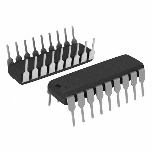
| 封装 | Tube |
| 封装/箱体 | MSOP-10 |
| 工厂包装数量 | 50 |
| 接口类型 | 3-Wire, SPI |
| 最大工作温度 | + 105 C |
| 最小工作温度 | - 40 C |
| 标准包装 | 50 |
| 电源电压-最大 | 5.5 V |
| 电源电压-最小 | 1.8 V |
| 稳定时间 | 7 us |
| 转换器数量 | 1 |
| 输出类型 | Voltage Buffered |
| 配用 | /product-detail/zh/EVAL-AD5683RSDZ/EVAL-AD5683RSDZ-ND/4875921 |


- 商务部:美国ITC正式对集成电路等产品启动337调查
- 曝三星4nm工艺存在良率问题 高通将骁龙8 Gen1或转产台积电
- 太阳诱电将投资9.5亿元在常州建新厂生产MLCC 预计2023年完工
- 英特尔发布欧洲新工厂建设计划 深化IDM 2.0 战略
- 台积电先进制程称霸业界 有大客户加持明年业绩稳了
- 达到5530亿美元!SIA预计今年全球半导体销售额将创下新高
- 英特尔拟将自动驾驶子公司Mobileye上市 估值或超500亿美元
- 三星加码芯片和SET,合并消费电子和移动部门,撤换高东真等 CEO
- 三星电子宣布重大人事变动 还合并消费电子和移动部门
- 海关总署:前11个月进口集成电路产品价值2.52万亿元 增长14.8%


PDF Datasheet 数据手册内容提取
Tiny 16-/14-/12-Bit SPI nanoDAC+, with ±2 (16-Bit) LSB INL and 2 ppm/°C Reference Data Sheet AD5683R/AD5682R/AD5681R/AD5683 FEATURES FUNCTIONAL BLOCK DIAGRAM Ultrasmall package: 2 mm × 2 mm, 8-lead LFCSP VLOGIC* VREF VDD High relative accuracy (INL): ±2 LSB maximum at 16 bits AD5683R/AD5682R/AD5681R LDAC PORWEESRE-TON 2R.E5VF AADD55668832RR// Low drift, 2.5 V reference: 2 ppm/°C typical AD5681R Selectable span output: 2.5 V or 5 V REF AD5683 RESET REGDIASCTER 16-/1D4-A/1C2-BIT OBUUFTFPEURT VOUT External reference only Selectable span output: V or 2 × V REF REF INPUT POWER-DOWN Total unadjusted error (TUE): 0.06% of FSR maximum CONTROL LOGIC CONTROL LOGIC NREETSWISOTORRK Offset error: ±1.5 mV maximum Gain error: ±0.05% of FSR maximum *NOT AVAILABLE IN ALL THE MODELS Low glitch: 0.1 nV-sec SYNC SCLK SDI SDO* GND 11955-001 High drive capability: 20 mA Figure 1. AD5683R/AD5682R/AD5681R MSOP Low power: 1.2 mW at 3.3 V (For more information, see the Functional Block Diagrams—LFCSP section.) Independent logic supply: 1.62 V logic compatible Wide operating temperature range: −40°C to +105°C Robust 4 kV HBM ESD protection APPLICATIONS Process controls Data acquisition systems Digital gain and offset adjustment Programmable voltage sources GENERAL DESCRIPTION Table 1. Single-Channel nanoDAC+ Portfolio The AD5683R/AD5682R/AD5681R/AD5683, members of the Interface Reference 16-Bit 14-Bit 12-Bit nanoDAC+® family, are low power, single-channel, 16-/14-/12-bit SPI Internal AD5683R AD5682R AD5681R buffered voltage out digital-to-analog converters (DACs). The External AD5683 devices, except the AD5683, include an enabled by default internal I2C Internal AD5693R AD5692R AD5691R 2.5 V reference, offering 2 ppm/°C drift. The output span can be External AD5693 programmed to be 0 V to V or 0 V to 2 × V . All devices REF REF operate from a single 2.7 V to 5.5 V supply and are guaranteed PRODUCT HIGHLIGHTS monotonic by design. The devices are available in a 2.00 mm × 1. High Relative Accuracy (INL). 2.00 mm, 8-lead LFCSP or a 10-lead MSOP. AD5683R/AD5683 (16-bit): ±2 LSB maximum. The internal power-on reset circuit ensures that the DAC register 2. Low Drift, 2.5 V On-Chip Reference. is written to zero scale at power-up while the internal output 2 ppm/°C typical temperature coefficient. buffer is configured in normal mode. The AD5683R/AD5682R 5 ppm/°C maximum temperature coefficient. /AD5681R/AD5683 contain a power-down mode that reduces 3. Two Package Options. the current consumption of the device to 2 µA (maximum) at 5 V 2.00 mm × 2.00 mm, 8-lead LFCSP. and provides software selectable output loads while in power- 10-lead MSOP. down mode. The AD5683R/AD5682R/AD5681R/AD5683 use a versatile 3-wire serial interface that operates at clock rates of up to 50 MHz. Some devices also include asynchronous RESET pin and V LOGIC pin options, allowing 1.8 V compatibility. Rev. D Document Feedback Information furnished by Analog Devices is believed to be accurate and reliable. However, no responsibility is assumed by Analog Devices for its use, nor for any infringements of patents or other One Technology Way, P.O. Box 9106, Norwood, MA 02062-9106, U.S.A. rights of third parties that may result from its use. Specifications subject to change without notice. No license is granted by implication or otherwise under any patent or patent rights of Analog Devices. Tel: 781.329.4700 ©2013–2016 Analog Devices, Inc. All rights reserved. Trademarks and registered trademarks are the property of their respective owners. Technical Support www.analog.com
AD5683R/AD5682R/AD5681R/AD5683 Data Sheet TABLE OF CONTENTS Features .............................................................................................. 1 Digital-to-Analog Converter .................................................... 19 Applications ....................................................................................... 1 Transfer Function ....................................................................... 19 Functional Block Diagram .............................................................. 1 DAC Architecture....................................................................... 19 General Description ......................................................................... 1 Serial Interface ................................................................................ 21 Product Highlights ........................................................................... 1 SPI Serial Data Interface ............................................................ 21 Revision History ............................................................................... 2 Short Write Operation (AD5681R Only) ................................ 21 Functional Block Diagrams—LFCSP............................................. 3 Internal Registers ........................................................................ 23 Specifications ..................................................................................... 4 Commands .................................................................................. 23 AC Characteristics ........................................................................ 6 Hardware LDAC ......................................................................... 25 Timing Characteristics ................................................................ 6 Hardware RESET ........................................................................ 25 Absolute Maximum Ratings ............................................................ 8 Thermal Hysteresis .................................................................... 26 Thermal Resistance ...................................................................... 8 Power-Up Sequence ................................................................... 26 ESD Caution .................................................................................. 8 Recommended Regulator .......................................................... 26 Pin Configurations and Function Descriptions ........................... 9 Layout Guidelines....................................................................... 26 Typical Performance Characteristics ........................................... 11 Outline Dimensions ....................................................................... 27 Terminology .................................................................................... 17 Ordering Guide .......................................................................... 28 Theory of Operation ...................................................................... 19 REVISION HISTORY 12/2016—Rev. C to Rev. D 10/2014—Rev. A to Rev. B Changed 1.8 V to 1.62 V, 1.8 V – 10% to 1.62 V, 5 V + 10% to 5.5 V, Changes to Table 1 ............................................................................. 1 and 1.8 V ≤ V ≤ 2.7 V to 1.62 V ≤ V ≤ 2.7 V ..... Throughout Changes to Figure 14 ...................................................................... 11 LOGIC LOGIC Changes to DC Power Supply Rejection Ratio, PSRR, Test Added Recommended Regulator Section ................................... 26 Conditions/Comments Column, Table 2 ......................................... 4 Changes to Ordering Guide .......................................................... 28 3/2016—Rev. B to Rev. C 1/2014—Rev. 0 to Rev. A Changes to Features Section............................................................ 1 Change to Features Section .............................................................. 1 Changes to Specifications Section .................................................. 4 Removed Endnote 2, Endnote 3, Endnote 5, and Endnote 6, Changes to Table 2 ............................................................................ 5 Table 2; Renumbered Sequentially .................................................. 5 Changes to AC Characteristics Section, Timing Characteristics Removed Endnote 2, Table 3; Renumbered Sequentially ............ 6 Section, and Table 4 .......................................................................... 6 Removed Endnote 1, Table 4; Renumbered Sequentially ............ 6 Changes to Figure 4 .......................................................................... 7 Changes to Table 5 ............................................................................. 8 Changes to Table 7 ............................................................................ 9 Removed Solder Heat Reflow Section and Figure 53; Changes to Table 8 .......................................................................... 10 Renumbered Sequentially ............................................................. 25 Changes to Terminology Section.................................................. 17 Changes to SPI Serial Data Interface Section ............................. 21 12/2013—Revision 0: Initial Version Rev. D | Page 2 of 28
Data Sheet AD5683R/AD5682R/AD5681R/AD5683 FUNCTIONAL BLOCK DIAGRAMS—LFCSP VLOGIC* VREF VDD POWER-ON AD5683R/ LDAC* RESET 2R.E5VF AD5682R/ AD5681R REF DAC OUTPUT REGISTER 16-/14-/12-BIT BUFFER VOUT RESET* DAC INPUT POWER-DOWN CONTROL LOGIC CONTROL LOGIC RESISTOR NETWORK *NOT AVAILABLE IN ALL THE MODELS SYNC SCLK SDI GND 11955-002 Figure 2. AD5683R/AD5682R/AD5681R LFCSP VREF VDD POWER-ON AD5683 RESET REF DAC OUTPUT LDAC* REGISTER 16-BIT BUFFER VOUT DAC INPUT POWER-DOWN CONTROL LOGIC CONTROL LOGIC RESISTOR NETWORK SYNC SCLK SDI GND 11955-003 Figure 3. AD5683 LFCSP Rev. D | Page 3 of 28
AD5683R/AD5682R/AD5681R/AD5683 Data Sheet SPECIFICATIONS V = 2.7 V to 5.5 V, R = 2 kΩ to GND, C = 200 pF to GND, V = 2.5 V, V = 1.62 V to 5.5 V, −40°C < T < +105°C, unless otherwise DD L L REF LOGIC A noted. Table 2. Parameter Min Typ Max Unit Test Conditions/Comments STATIC PERFORMANCE1 AD5683R Resolution 16 Bits Relative Accuracy, INL LSB A Grade ±8 LSB B Grade ±2 LSB Gain = 2 ±3 Gain = 1 Differential Nonlinearity, DNL ±1 LSB Guaranteed monotonic by design AD5683 Resolution 16 Bits Relative Accuracy, INL ±2 LSB Gain = 2 ±3 LSB Gain =1 Differential Nonlinearity, DNL ±1 LSB Guaranteed monotonic by design AD5682R Resolution 14 Bits Relative Accuracy, INL ±1 LSB Differential Nonlinearity, DNL ±1 LSB Guaranteed monotonic by design AD5681R Resolution 12 Bits Relative Accuracy, INL ±1 LSB Differential Nonlinearity, DNL ±1 LSB Guaranteed monotonic by design Zero-Code Error 1.25 mV All 0s loaded to DAC register Offset Error ±1.5 mV Full-Scale Error ±0.075 % of FSR All 1s loaded to DAC register Gain Error ±0.05 % of FSR Total Unadjusted Error, TUE ±0.16 % of FSR Internal reference, gain = 1 ±0.14 % of FSR Internal reference, gain = 2 ±0.075 % of FSR External reference, gain = 1 ±0.06 % of FSR External reference, gain = 2 Zero-Code Error Drift ±1 µV/°C Offset Error Drift ±1 µV/°C Gain Temperature Coefficient ±1 ppm/°C DC Power Supply Rejection Ratio, PSRR 0.2 mV/V DAC code = midscale; V = 5 V DD OUTPUT CHARACTERISTICS Output Voltage Range 0 V V Gain = 1 REF 0 2 × V V Gain = 2 REF Capacitive Load Stability 2 nF R = ∞ L 10 nF R = 2 kΩ L Resistive Load 1 kΩ C = 0 µF L Load Regulation 10 µV/mA 5 V, DAC code = midscale; −30 mA ≤ I ≤ +30 mA OUT 10 µV/mA 3 V, DAC code = midscale; −20 mA ≤ I ≤ +20 mA OUT Short-Circuit Current 20 30 50 mA Load Impedance at Rails2 20 Ω Rev. D | Page 4 of 28
Data Sheet AD5683R/AD5682R/AD5681R/AD5683 Parameter Min Typ Max Unit Test Conditions/Comments REFERENCE OUTPUT Output Voltage 2.4975 2.5025 V At ambient Voltage Reference TC3 See the Terminology section A-Grade 5 20 ppm/°C B-Grade 2 5 ppm/°C Output Impedance 0.05 Ω Output Voltage Noise 16.5 µV p-p 0.1 Hz to 10 Hz Output Voltage Noise Density 250 nV/√Hz At ambient; f = 10 kHz, C = 10 nF L Capacitive Load Stability 5 µF R = 2 kΩ L Load Regulation Sourcing 50 µV/mA At ambient; V ≥ 3 V DD Load Regulation Sinking 30 µV/mA At ambient Output Current Load Capability ±5 mA V ≥ 3 V DD Line Regulation 80 µV/V At ambient Thermal Hysteresis 125 ppm First cycle 25 ppm Additional cycles REFERENCE INPUT Reference Current 26 µA V = V = V = 5 V, gain = 1 REF DD LOGIC 47 µA V = V = V = 5 V, gain = 2 REF DD LOGIC Reference Input Range 1 V V DD Reference Input Impedance 120 kΩ Gain = 1 60 kΩ Gain = 2 LOGIC INPUTS I , Input Current ±1 µA Per pin IN V , Input Low Voltage4 0.3 × V V INL DD V , Input High Voltage4 0.7 × V V INH DD C , Pin Capacitance 2 pF IN LOGIC OUTPUTS (SDO)5 Output Low Voltage, V 0.4 V I = 200 μA OL SINK Output High Voltage, V V − 0.4 V I = 200 μA OH DD SOURCE Pin Capacitance 4 pF POWER REQUIREMENTS V 5 1.62 5.5 V LOGIC I 5 0.25 3 µA V = V or V = GND LOGIC IH LOGIC IL V 2.7 5.5 V Gain = 1 DD V + 1.5 5.5 V Gain = 2 REF I 6 V = V , V = GND DD IH DD IL Normal Mode7 350 500 µA Internal reference enabled 110 180 µA Internal reference disabled Power-Down Modes8 2 µA 1 Linearity is calculated using a reduced code range: AD5683R and AD5683 (Code 512 to Code 65,535); AD5682R (Code 128 to Code 16,384); AD5681R (Code 32 to Code 4096). Output unloaded. 2 When drawing a load current at either rail, the output voltage headroom, with respect to that rail, is limited by the 20 Ω typical channel resistance of the output devices; for example, when sinking 1 mA, the minimum output voltage = 20 Ω, 1 mA generates 20 mV. See Figure 38 (Headroom/Footroom vs. Load Current). 3 Reference temperature coefficient is calculated as per the box method. See the Terminology section for more information. 4 Substitute VLOGIC for VDD if device includes a VLOGIC pin. 5 The VLOGIC and SDO pins are not available on all models. 6 If the VLOGIC pin is not available, IDD = IDD + ILOGIC. 7 Interface inactive. DAC active. DAC output unloaded. 8 DAC powered down. Rev. D | Page 5 of 28
AD5683R/AD5682R/AD5681R/AD5683 Data Sheet AC CHARACTERISTICS V = 2.7 V to 5.5 V, R = 2 kΩ to GND, C = 200 pF to GND, V = 2.5 V, V = 1.62 V to 5.5 V, −40°C < T < +105°C, unless otherwise DD L L REF LOGIC A noted.1 Table 3. Parameter Typ Max Unit Test Conditions/Comments Output Voltage Settling Time2, 3 5 7 µs Gain = 1 Slew Rate 0.7 V/µs Digital-to-Analog Glitch Impulse2 0.1 nV-sec ±1 LSB change around major carry, gain = 2 Digital Feedthrough2 0.1 nV-sec Total Harmonic Distortion2 −83 dB V = 2 V ± 0.1 V p-p, frequency = 10 kHz REF Output Noise Spectral Density 200 nV/√Hz DAC code = midscale, 10 kHz Output Noise 6 µV p-p 0.1 Hz to 10 Hz; internal reference, DAC = zero scale SNR 90 dB At ambient, BW = 20 kHz, V = 5 V, f = 1 kHz DD OUT SFDR 88 dB At ambient, BW = 20 kHz, V = 5 V, f = 1 kHz DD OUT SINAD 82 dB At ambient, BW = 20 kHz, V = 5 V, f = 1 kHz DD OUT 1 Temperature range = −40°C to +105°C, typical at 25°C. 2 See the Terminology section. 3 AD5683R/AD5683 to ±2 LSB, AD5682R to ±1 LSB, AD5681R to ±0.5 LSB. TIMING CHARACTERISTICS V = 2.7 V to 5.5 V, V = 1.62 V to 5.5 V, −40°C < T < +105°C, unless otherwise noted. DD LOGIC A Table 4. 1.62 V ≤ V ≤ 2.7 V 2.7 V ≤ V 2 ≤ 5.5 V Daisy Chain and Readback LOGIC LOGIC Parameter 1 Symbol Min Typ Max Min Typ Max Min Typ Max Unit SCLK Cycle Time t 33 20 40 ns 1 SCLK High Time t 16 10 20 ns 2 SCLK Low Time t 16 10 20 ns 3 SYNC to SCLK Falling Edge Setup Time t4 15 10 20 ns Data Setup Time t 5 5 5 ns 5 Data Hold Time t 5 5 5 ns 6 SCLK Falling Edge to SYNC Rising Edge t7 15 10 10 ns Minimum SYNC High Time t8 20 20 40 ns SYNC Falling Edge to SCLK Fall Ignore t9 16 10 10 ns SDO Data Valid from SCLK Rising Edge t 35 ns 10 SYNC Rising Edge to SCLK Falling Edge t11 10 ns SYNC Rising Edge to SDO Disabled t12 60 ns SYNC Rising Edge to LDAC Falling Edge t13 25 25 25 ns LDAC Pulse Width Low t14 20 15 15 ns RESET Minimum Pulse Width Low t15 75 75 75 ns RESET Pulse Activation Time t16 150 150 150 ns SYNC Rising Edge to SYNC Rising Edge t17 1.9 1.7 1.7 µs (DAC Updates) LDAC Falling Edge to SYNC Rising Edge t18 1.8 1.65 1.65 µs Reference Power-Up3 t 4 600 600 600 µs REF_POWER_UP Exit Shutdown3 t 5 6 6 6 µs SHUTDOWN 1 All input signals are specified with tR = tF = 1 ns/V (10% to 90% of VDD) and timed from a voltage level of (VIL + VIH)/2. 2 Substitute VDD for VLOGIC on devices that do not include a VLOGIC pin. 3 Not shown in Figure 4. 4 Same timing must be expected when powering up the device after VDD = 2.7 V. 5 Time required to exit power-down to normal mode of AD5683R/AD5682R/AD5681R operation; SYNC rising edge to 90% of DAC midscale value, with output unloaded. Rev. D | Page 6 of 28
Data Sheet AD5683R/AD5682R/AD5681R/AD5683 Timing and Circuit Diagrams t4 t9 t2 t1 t7 SCLK t8 t3 t11 SYNC t17 t5 t6 SDI DB23 DB22 DB21 DB20 DB2 DB1 DB0 t10 t12 SDO DB23 DB22 DB21 DB20 DB2 DB1 DB0 t13 t14 LDAC t18 t15 RESET t16 VOUT 11955-004 Figure 4. SPI Timing Diagram, Compatible with Mode 1 and Mode 2 (See the AN-1248 Application Note) 200µA IOL TO OUTPPUINT VOH (MIN) CL 90pF 200µA IOH 11955-005 Figure 5. Load Circuit for Digital Output (SDO) Timing Specifications Rev. D | Page 7 of 28
AD5683R/AD5682R/AD5681R/AD5683 Data Sheet ABSOLUTE MAXIMUM RATINGS T = 25°C, unless otherwise noted. A Stresses at or above those listed under Absolute Maximum Ratings may cause permanent damage to the product. This is a Table 5. stress rating only; functional operation of the product at these Parameter Rating or any other conditions above those indicated in the operational V to GND −0.3 V to +7 V DD section of this specification is not implied. Operation beyond V to GND −0.3 V to +7 V LOGIC the maximum operating conditions for extended periods may V to GND −0.3 V to V + 0.3 V or +7 V OUT DD (whichever is less) affect product reliability. V to GND −0.3 V to V + 0.3 V or +7 V THERMAL RESISTANCE REF DD (whichever is less) θ is defined by the JEDEC JESD51 standard, and the value is Digital Input Voltage to GND1 −0.3 V to V + 0.3 V or +7 V JA DD (whichever is less) dependent on the test board and test environment. Operating Temperature Range Table 6. Thermal Resistance1 Industrial −40°C to +105°C Package Type θ θ Unit JA JC Storage Temperature Range −65°C to +150°C 8-Lead LFCSP 90 25 °C/W Junction Temperature (T max) 135°C J 10-Lead MSOP 135 N/A °C/W Power Dissipation (T max − T )/θ J A JA ESD2 4 kV 1 JEDEC 2S2P test board, still air (0 m/sec airflow). FICDM3 1.25 kV ESD CAUTION 1 Substitute VDD with VLOGIC on devices that include a VLOGIC pin. 2 Human body model (HBM) classification. 3 Field-Induced Charged-Device Model classification. Rev. D | Page 8 of 28
Data Sheet AD5683R/AD5682R/AD5681R/AD5683 PIN CONFIGURATIONS AND FUNCTION DESCRIPTIONS VDD 1 AD5681R/ 8 VOUT AD5682R/ LDAC 2 AD5683R/ 7 VREF AD5683 GND 3 6 SDI TOP VIEW (Not to Scale) SCLK 4 5 SYNC N1.O CTOENSNECT THE EXPOSED PAD TO GND. 11955-006 Figure 6. Pin Configuration, 8-Lead LFCSP, LDAC Option VDD 1 8 VOUT VLOGIC 2 AD5683R-1/ 7 VREF AD5681R-1 GND 3 6 SDI TOP VIEW (Not to Scale) SCLK 4 5 SYNC N1.O CTOENSNECT THE EXPOSED PAD TO GND. 11955-007 Figure 7. Pin Configuration, 8-Lead LFCSP, VLOGIC Option VDD 1 8 VOUT RESET 2 7 VREF AD5683R-2 GND 3 6 SDI TOP VIEW (Not to Scale) SCLK 4 5 SYNC N1.O CTOENSNECT THE EXPOSED PAD TO GND. 11955-008 Figure 8. Pin Configuration, 8-Lead LFCSP, RESET Option Table 7. Pin Function Descriptions, 8-Lead LFCSP Pin No. LDAC V RESET Mnemonic Description LOGIC 1 1 1 V Power Supply Input. These devices can be operated from 2.7 V to 5.5 V. Decouple the supply to GND. DD 2 N/A N/A LDAC LDAC can be operated in asynchronous mode (see Figure 4). Pulsing this pin low allows the DAC register to be updated if the input register has new data. This pin can be tied permanently low; in this case, the DAC is automatically updated when new data is written to the input register. N/A 2 N/A V Digital Power Supply. Voltage ranges from 1.62 V to 5.5 V. LOGIC N/A N/A 2 RESET Asynchronous Reset Input. The RESET input is low level sensitive. When RESET is low, all LDAC pulses are ignored, the input and DAC registers are at their default values, and the output is connected to GND. Data written to the AD5683R is ignored. If not used, this pin can be tied to V . LOGIC 3 3 3 GND Ground Reference Point for All Circuitry on the Device. 4 4 4 SCLK Serial Clock Input. Data is clocked into the input shift register on the falling edge of the serial clock input. Data can be transferred at rates of up to 50 MHz. 5 5 5 SYNC Active Low Control Input. This is the frame synchronization signal for the input data. When SYNC goes low, it powers on the SCLK and SDI buffers and enables the input shift register. Data is transferred in on the falling edges of the next 24 clocks. 6 6 6 SDI Serial Data Input. This device has a 24-bit shift register. Data is clocked into the register on the falling edge of the serial clock input. 7 7 7 V AD5683R/AD5682R/AD5681R Reference Output. When using the internal reference, this is the REF reference output pin. The default for this pin is as a reference output. It is recommended that this pin be decoupled to GND with a 10 nF capacitor. 8 8 8 V Analog Output Voltage from the DAC. The output amplifier has rail-to-rail operation. OUT 0 0 0 EPAD Exposed Pad. Connect the exposed pad to GND. Rev. D | Page 9 of 28
AD5683R/AD5682R/AD5681R/AD5683 Data Sheet VDD 1 10 VOUT VDD 1 10 VOUT VLOGIC 2 AD5683R/ 9 VREF RESET 2 AD5683R-3 9 VREF AD5681R RESET 3 8 SDI SDO 3 8 SDI TOP VIEW TOP VIEW LGDANCD 45 (Not to Scale) 76 SSYCNLKC 11955-009 LGDANCD 45 (Not to Scale) 76 SSYCNLKC 11955-010 Figure 9. Pin Configuration, 10-Lead MSOP, VLOGIC Option Figure 10. Pin Configuration, 10-Lead MSOP, SDO Option Table 8. Pin Function Descriptions, 10-Lead MSOP V SDO Mnemonic Description LOGIC 1 1 V Power Supply Input. These devices can be operated from 2.7 V to 5.5 V. Decouple this pin to GND. DD 2 N/A V Digital Power Supply. Voltage ranges from 1.62 V to 5.5 V. Decouple this pin to GND. LOGIC 3 2 RESET Hardware Reset Pin. The RESET input is low level sensitive. When RESET is low, the device is reset and external pins are ignored. The input and DAC registers are loaded with a zero-scale value, and the write control register is loaded with default values. If not used, tie this pin to V . LOGIC N/A 3 SDO Serial Data Output. Can be used for daisy chaining or readback commands. 4 4 LDAC Load DAC. Transfers the content of the input register to the DAC register. It can be operated in asynchronous mode (see Figure 4). This pin can be tied permanently low; in this case, the DAC register is automatically updated when new data is written to the input register. 5 5 GND Ground Reference. 6 6 SCLK Serial Clock Input. Data is clocked into the input shift register on the falling edge of the serial clock input. Data can be transferred at rates of up to 50 MHz. 7 7 SYNC Synchronization Data Input. When SYNC goes low, it enables the SCLK and SDI buffers and the input shift register. 8 8 SDI Serial Data Input. Data is sampled on the falling edge of SCLK. 9 9 V Reference Input/Output. When using the internal reference, this is the reference output pin. The default REF for this pin is as a reference output. It is recommended that this pin be decoupled to GND with a 10 nF capacitor. 10 10 V Analog Output Voltage from the DAC. The output amplifier has rail-to-rail operation. OUT Rev. D | Page 10 of 28
Data Sheet AD5683R/AD5682R/AD5681R/AD5683 TYPICAL PERFORMANCE CHARACTERISTICS 2 2 VDD = 5V VDD = 5V TA = 25°C TA = 25°C VREF = 2.5V VREF = 2.5V 1 1 B) B) S S NL (L 0 NL (L 0 I D –1 –1 –20 10000 20000 300C0O0DE40000 50000 600006553511955-011 –20 10000 20000 300C0O0DE40000 50000 6000065535 11955-014 Figure 11. AD5683R/AD5683 INL Figure 14. AD5683R/AD5683 DNL 2 1.0 VDD = 5V VDD = 5V TA = 25°C 0.8 TA = 25°C VREF = 2.5V VREF = 2.5V 0.6 1 0.4 B) B) 0.2 S S NL (L 0 NL (L 0 I D–0.2 –0.4 –1 –0.6 –0.8 –20 2000 4000 6000 8C0O0D0E10000 12000 14000 16383 11955-012 –1.00 2000 4000 6000 8C0O0D0E10000 12000 14000 1638311955-015 Figure 12. AD5682R INL Figure 15. AD5682R DNL 2.0 1.0 VDD = 5V VDD = 5V 1.5 TVAR E=F 2=5 °2C.5V 0.8 TVAR E=F 2=5 °2C.5V 0.6 1.0 0.4 0.5 B) B) 0.2 S S NL (L 0 NL (L 0 I D–0.2 –0.5 –0.4 –1.0 –0.6 –1.5 –0.8 –2.00 500 1000 1500 2C0O00DE2500 3000 3500 4000 11955-013 –1.00 500 1000 1500 2C0O00DE2500 3000 3500 4000 11955-016 Figure 13. AD5681R INL Figure 16. AD5681R DNL Rev. D | Page 11 of 28
AD5683R/AD5682R/AD5681R/AD5683 Data Sheet 1.2 1.4 VDD = 5V U1_DNL U2_DNL VDD = 5V VREF = 2.5V U3_DNL U1_INL TA = 25°C 1.0 1.2 U2_INL U3_INL B) B) 1.0 S 0.8 S L L OR ( OR ( 0.8 R 0.6 R R R DNL E 0.4 UU13__DDNNLL__IINNTT UU21__DDNNLL__IENXTT DNL E 0.6 ND UU21__DINNLL__INETXT UU32__DINNLL__INETXT ND 0.4 A U3_INL_INT U1_INL_EXT A NL 0.2 U2_INL_EXT U3_INL_EXT NL 0.2 I I 0 0 –0.2 –40 –20 0 TEMP2E0RATU4R0E (°C)60 80 105 11955-017 –0.22 3 VREF (V) 4 5 11955-020 Figure 17. INL and DNL Error vs. Temperature (AD5683R/AD5683) Figure 20. INL Error and DNL Error vs. VREF (AD5683R/AD5683) 1.4 0.02 U1_DNL_INT U2_DNL_INT TA = 25°C U3_DNL_INT U1_DNL_EXT 1.2 UU21__DINNLL__INETXT UU32__DINNLL__INETXT 0.01 U3_INL_INT U1_INL_EXT SB) 1.0 U2_INL_EXT U3_INL_EXT 0 RROR (L 0.8 E (% FSR)–0.01 NL E 0.6 TU–0.02 D D 0.4 N A –0.03 L N 0.2 I –0.04 –0.20 000 120500000000 2410000000000 3610050C00000O0DE4820000000000 15200500000000 1632000000000016465035983535 (((AAADDD555666888213RR/A))D5683R) 11955-021 2.70 3.30 3.75 VDD 4(V.2)5 4.75 5.25 11955-018 Figure 18. INL and DNL Error vs. Supply Voltage Figure 21. TUE vs. Code 0.06 0.04 U1_EXT VDD = 5V TA = 25°C U2_EXT GAIN = 1 GAIN = 1 UU31__EINXTT VREF = 2.5V 0.03 VREF = 2.5V 0.04 U2_INT U3_INT 0.02 R)0.02 R) S S F F % % 0.01 E ( E ( TU 0 TU 0 –0.02 –0.01 U1_INT U1_EXT U2_INT U2_EXT U3_INT U3_EXT –0.04 –40 0 TEMPERATUR40E (°C) 80 11955-019 –0.02 2.70 3.30 3.75 VDD 4(V.2)5 4.75 5.25 11955-022 Figure 19. TUE vs. Temperature Figure 22. TUE vs. Supply Rev. D | Page 12 of 28
Data Sheet AD5683R/AD5682R/AD5681R/AD5683 0.03 0.030 TA = 25°C 0.025 GAIN = 1 0.02 VREF = 2.5V 0.020 0.01 0.015 R) R) 0.010 S S % F 0 % F 0.005 ROR (–0.01 ROR ( 0 ER ER–0.005 U1_INT –0.02 –0.010 U2_INT U3_INT –0.015 –0.03 U1_EXT VDD = 5V U1_INT U1_EXT U2_EXT GAIN = 1 –0.020 U2_INT U2_EXT U3_EXT VREF = 2.5V U3_INT U3_EXT –0.04 –40 0 TEMPERATUR40E (°C) 80 11955-023 –0.025 2.70 3.30 3.75 VD4D.2 5(V) 4.75 5.25 5.50 11955-026 Figure 23. Gain Error and Full-Scale Error vs. Temperature Figure 26. Gain Error and Full-Scale Error vs. Supply 350 500 VDD = 5V U1_INT TA = 25°C GAIN = 1 U2_INT GAIN = 1 300 VREF = 2.5V U3_INT VREF = 2.5V 400 U1_EXT U2_EXT 250 U3_EXT V) V) 300 R (µ 200 R (µ O O R R ER 150 ER 200 100 U1_INT U2_INT U3_INT 100 50 U1_EXT U2_EXT U3_EXT 0 –40 –20 0 TEMP2E0RATU4R0E (°C)60 80 105 11955-024 0 2.70 3.30 3.75 VD4D.2 5(V) 4.75 5.25 5.50 11955-027 Figure 24. Zero Code Error and Offset Error vs. Temperature Figure 27. Zero Code Error and Offset Error vs. Supply 2.505 4.5 U1 VDD = 5V VDD = 5V U2 4.0 TA = 25°C U3 GAIN = 1 2.503 3.5 S 3.0 T 2.501 HI (V)F R OF 2.5 VRE2.499 MBE 2.0 U N 1.5 1.0 2.497 0.5 0 2.495–40 1T0EMPERATURE (°C)60 11955-025 2.500012.500042.500072.500102.500132.500162.500192.500222.500252.500282.500312.500342.500372.500402.50043V2.50046R2.50049EF2.50052 (2.50055V)2.500582.500612.500642.500672.500702.500732.500762.500792.500822.500852.500882.500912.500942.500972.50100 11955-028 Figure 25. Internal Reference Voltage vs. Temperature (Grade B) Figure 28. Reference Output Spread Rev. D | Page 13 of 28
AD5683R/AD5682R/AD5681R/AD5683 Data Sheet 2.50015 2.5009 TA = 25°C TA = 25°C 5.5V 5.0V 2.50010 3.0V 2.5008 2.7V 2.50005 2.5007 V) 2.50000 V) V (REF2.49995 V (REF 2.5006 2.5005 2.49990 2.49985 D11 2.5004 D12 D13 2.49980 2.5003 2.5 3.5 VDD (V) 4.5 5.5 11955-029 –0.005 –0.003 L–O0.A0D01 CURRE0N.T00 (1A) 0.003 0.005 11955-032 Figure 29. Internal Reference Voltage vs. Supply Voltage Figure 32. Internal Reference Voltage vs. Load Current 1800 T TVAD D= =2 55°VC 1600 TVAD D= =2 55°VC z) H V/√ 1400 n D ( 1200 S N E C 1000 1 EN ER 800 F E L R 600 A N R 400 E T N I 200 CH1 10µV M1.00s A CH1 2.00µV 11955-030 010 100 FR1kEQUENCY 1(H0kz) 100k 1M 11955-033 Figure 30. Internal Reference Noise, 0.1 Hz to 10 Hz Figure 33. Internal Reference Noise Spectral Density vs. Frequency T TA = 25°C T TA = 25°C VDD = 5V VDD = 5V 1 1 CH1 10µV M1.00s A CH1 2.00µV 11955-031 CH1 10µV M1.00s A CH1 2.00µV 11955-034 Figure 31. 0.1 Hz to 10 Hz Output Noise Plot, Internal Reference On Figure 34. 0.1 Hz to 10 Hz Output Noise Plot, External Reference Rev. D | Page 14 of 28
Data Sheet AD5683R/AD5682R/AD5681R/AD5683 1200 1.4 FMZUEIDRLSLOC-SSACCLAAELLEE VTGADA DI=N =2 =55 °V1C 1.0 SSIONUKRINCGIN, GV,D VD D=D 3 =V 5V TA = 25°C 1000 SINKING, VDD = 5V SOURCING, VDD = 3V 0.6 800 SD (nV/√Hz) 600 ΔV (V)OUT–00..22 N 400 –0.6 200 –1.0 010 100 FR1kEQUENCY 1(H0kz) 100k 1M 11955-035 –1.40 0.0L1OAD CURRENT (A0).02 0.03 11955-038 Figure 35. Noise Spectral Density vs. Frequency, Gain = 1 Figure 38. Headroom/Footroom vs. Load Current 6 7 0xFFFF VDD = 5V 0xFFFF VDD = 5V 0xC000 TA = 25°C 6 0xC000 TA = 25°C 5 0x8000 GAIN = 1 0x8000 GAIN = 2 0x4000 0x4000 0x0000 5 0x0000 4 4 V) 3 V) 3 (T (T U U VO 2 VO 2 1 1 0 0 –1 –1–50 LOAD CUR0RENT (mA) 50 11955-036 –2–50 LOAD CUR0RENT (mA) 50 11955-039 Figure 36. Source and Sink Capability, Gain = 1 Figure 39. Source and Sink Capability, Gain = 2 500 0.0015 VDD = 5V GAIN = 1 VDD = 5V 450 0.0010 GAIN = 2 TA = 25°C REFERENCE = 2.5V 400 CODE = 0x7FFF TO 0x8000 0.0005 350 0 300 I (µA)DD225000 ZFFSSS___IEINNXTTT___GGGAAAIINNIN == = 12 2 ZFFSSS___IIENNXTTT___GGGAAAIINNIN == = 21 1 V (V)OUT–0.0005 –0.0010 150 –0.0015 100 –0.0020 50 0 –40 –20 0 TEMP2E0RATU4R0E (°C)60 80 105 11955-037 –0.00250 1 2 3TIME (µs4) 5 6 7 11955-040 Figure 37. Supply Current vs. Temperature Figure 40. Digital-to-Analog Glitch Impulse Rev. D | Page 15 of 28
AD5683R/AD5682R/AD5681R/AD5683 Data Sheet 2.5 4.5 0nF 0nF 0.2nF 4.0 0.2nF 1nF 1nF 2.0 4.7nF 3.5 4.7nF 10nF 10nF 3.0 1.5 V) V) 2.5 (T (T U U VO VO 2.0 1.0 1.5 0.5 VTAD D= =2 55°VC 1.0 VTAD D= =2 55°VC GAIN = 1 GAIN = 2 0.5 RL = 2kΩ RL = 2kΩ INTERNAL REFERENCE = 2.5V INTERNAL REFERENCE = 2.5V 00 TIM0E.0 (1ms) 0.02 11955-041 00 TIM0E.0 (1ms) 0.02 11955-044 Figure 41. Capacitive Load vs. Settling Time, Gain = 1 Figure 44. Capacitive Load vs. Settling Time, Gain = 2 20 0 VDD = 5V GAIN = 2 TINAT =E R25N°ACL REFERENCE = 2.5V –10 GAIN = 1 V) B –30 –20 d N ( B) O d –30 STORTI –80 WIDTH ( –40 DI D C AN –50 NI B O M AR –130 –60 H VDD = 5V –70 TA = 25°C VOUT = MIDSCALE EXTERNAL REFERENCE = 2.5V, ±0.1V p-p –80 –1800 5 FREQUE1N0CY (kHz) 15 20 11955-042 1k 10k FREQU1E0N0kCY (Hz) 1M 10M 11955-045 Figure 42. Total Harmonic Distortion at 1 kHz Figure 45. Multiplying Bandwidth, External Reference 2.5 V ± 0.1 V p-p, 10 kHz to 10 MHz 6 0.06 3 VDD = 5V TA = 25°C MIDSCALE, GAIN = 2 5 0.05 4 0.04 2 VDD V (V)DD 32 00..0032 V (V)OUT V (V)OUT SYNC MIDSCALE, GAIN = 1 1 1 0.01 VOUT 0 0 –10 1 2 3 TIME4 (ms) 5 6 7 8–0.01 11955-043 0–5 0 TIME5 (µs) 10 15 11955-046 Figure 43. Power-On Reset to 0 V Figure 46. Exiting Power-Down to Midscale Rev. D | Page 16 of 28
Data Sheet AD5683R/AD5682R/AD5681R/AD5683 TERMINOLOGY Relative Accuracy or Integral Nonlinearity (INL) Output Voltage Settling Time For the DAC, relative accuracy or integral nonlinearity is a Output voltage settling time is the amount of time it takes for measurement of the maximum deviation, in LSBs, from a straight the output of a DAC to settle to a specified level for a ¼ to ¾ line passing through the endpoints of the DAC transfer function. scale input change. See Figure 11, Figure 12, and Figure 13 for typical INL vs. Digital-to-Analog Glitch Impulse code plots. Digital-to-analog glitch impulse is the impulse injected into the Differential Nonlinearity (DNL) analog output when the input code in the DAC register changes Differential nonlinearity is the difference between the measured state. It is normally specified as the area of the glitch in nV-sec change and the ideal 1 LSB change between any two adjacent and is measured when the digital input code is changed by 1 LSB codes. A specified differential nonlinearity of ±1 LSB maximum at the major carry transition (0x7FFF to 0x8000), as shown in ensures monotonicity. This DAC is guaranteed monotonic by Figure 40. design. See Figure 14, Figure 15, and Figure 16 for typical DNL Digital Feedthrough vs. code plots. Digital feedthrough is a measure of the impulse injected into Zero Code Error the analog output of the DAC from the digital inputs of the Zero code error is a measurement of the output error when zero DAC, but it is measured when the DAC output is not updated. code (0x0000) is loaded to the DAC register. Ideally, the output Digital feedthrough is specified in nV-sec and measured with must be 0 V. The zero code error is always positive in the a full-scale code change on the data bus, that is, from all 0s to all AD5683R/AD5682R/AD5681R because the output of the DAC 1s and vice versa. cannot fall below 0 V due to a combination of the offset errors Reference Feedthrough in the DAC and the output amplifier. Zero code error is expressed Reference feedthrough is the ratio of the amplitude of the signal in mV. A plot of zero code error vs. temperature is shown in at the DAC output to the reference input when the DAC output Figure 24. is not being updated. It is expressed in dB. Full-Scale Error Output Noise Spectral Density Full-scale error is a measurement of the output error when full- Noise spectral density is a measurement of the internally generated scale code (0xFFFF) is loaded to the DAC register. Ideally, the random noise. Random noise is characterized as a spectral density output must be V – 1 LSB or |2 × V | – 1 LSB. Full-scale error is REF REF (nV/√Hz). It is measured by loading the DAC to midscale and expressed in percent of full-scale range (% of FSR). See Figure 23 measuring noise at the output. It is measured in nV/√Hz. See and Figure 26 for plots of full-scale error. Figure 31, Figure 34, and Figure 35 for a plot of noise spectral Gain Error density. The noise spectral density for the internal reference is Gain error is a measure of the span error of the DAC. It is the shown in Figure 30 and Figure 33. deviation in slope of the DAC transfer characteristic from the Multiplying Bandwidth ideal expressed as % of FSR. The amplifiers within the DAC have a finite bandwidth. The Zero-Code Error Drift multiplying bandwidth is a measure of this finite bandwidth. Zero-code error drift is a measurement of the change in zero- A sine wave on the reference (with full-scale code loaded to the code error with a change in temperature. It is expressed in µV/°C. DAC) appears on the output. The multiplying bandwidth is the frequency at which the output amplitude falls to 3 dB below Gain Temperature Coefficient the input. Gain temperature coefficient is a measurement of the change in gain error with changes in temperature. It is expressed in ppm Total Harmonic Distortion (THD) of FSR/°C. THD is the difference between an ideal sine wave and the attenuated version using the DAC. The sine wave is used as the Offset Error reference for the DAC, and the THD is a measurement of the Offset error is a measure of the difference between V (actual) OUT harmonics present on the DAC output. It is measured in dB. and V (ideal) expressed in mV in the linear region of the OUT transfer function. Offset error is measured on the AD5683R with Code 512 loaded in the DAC register. It can be negative or positive. DC Power Supply Rejection Ratio (PSRR) PSRR indicates how the output of the DAC is affected by changes in the supply voltage. PSRR is the ratio of the change in V to OUT a change in V for mid-scale output of the DAC. It is measured DD in dB. V is held at 2 V, and V is varied by ±10%. REF DD Rev. D | Page 17 of 28
AD5683R/AD5682R/AD5681R/AD5683 Data Sheet Voltage Reference Temperature Coefficient (TC) Thermal Hysteresis Voltage reference TC is a measure of the change in the reference Thermal hysteresis is the voltage difference induced on the output voltage with a change in temperature. The reference TC reference voltage by sweeping the temperature from ambient is calculated using the box method, which defines the TC as the to cold, to hot, and then back to ambient. maximum change in the reference output over a given tempera- ture range expressed in ppm/°C, as follows: V −V TC= REFmax REFmin ×106 VREFnom×TempRange where: V is the maximum reference output measured over the REFmax total temperature range. V is the minimum reference output measured over the total REFmin temperature range. V is the nominal reference output voltage, 2.5 V. REFnom TempRange is the specified temperature range, −40°C to +105°C. Rev. D | Page 18 of 28
Data Sheet AD5683R/AD5682R/AD5681R/AD5683 THEORY OF OPERATION DIGITAL-TO-ANALOG CONVERTER The simplified segmented resistor string DAC structure is shown in Figure 48. The code loaded to the DAC register The AD5683R/AD5682R/AD5681R are single 16-bit, 14-bit, and determines the switch on the string that is connected to the 12-bit, serial input, voltage output DACs with a 2.5 V internal output buffer. reference. The devices operate from supply voltages of 2.7 V to 5.5 V. Data is written to the AD5683R/AD5682R/AD5681R in Because each resistance in the string has same value, R, the a 24-bit word format via a 3-wire serial interface. The AD5683R/ string DAC is guaranteed monotonic. AD5682R/AD5681R incorporate a power-on reset circuit that VREF ensures that the DAC output powers up to a zero scale. The devices also have a software power-down mode that reduces the typical R current consumption to 2 µA maximum. TRANSFER FUNCTION R The internal reference is on by default. For users that need an R TO OUTPUT external reference, the AD5683 is available. The input coding to BUFFER the DAC is straight binary. The ideal output voltage is given by the following equations: For the AD5683R, V (D) = Gain × V × D R OUT REF 65,536 For the AD5682R, R VOUT(D) = Gain × VREF × 16,D384 11955-048 Figure 48. Simplified Resistor String Structure For the AD5681R, Internal Reference V (D) = Gain × V × D OUT REF The AD5683R/AD5682R/AD5681R on-chip reference is on at 4096 power-up but can be disabled via a write to the write control where: register. D is the decimal equivalent of the binary code that is loaded to the DAC register. The AD5683R/AD5682R/AD5681R each have a 2.5 V, 2 ppm/°C Gain is the gain of the output amplifier. By default, it is set to reference, giving a full-scale output of 2.5 V or 5 V, depending ×1. The gain can also be set to ×2 using the gain bit in the write on the state of the gain bit. control register. The internal reference is available at the V pin. It is internally REF DAC ARCHITECTURE buffered and capable of driving external loads of up to 50 mA. External Reference The AD5683R/AD5682R/AD5681R/AD5683 implements segmented string DAC architecture with an internal output The V pin is an input pin in the AD5683. It can also be con- REF buffer. Figure 47 shows the internal block diagram. figured as an input pin on the AD5683R/AD5682R/AD5681R, VREF allowing the use of an external reference if the application 2.5V requires it. REF In the AD5683R/AD5682R/AD5681R, the default condition of REF (+) INPUT DAC RESISTOR the on-chip reference is on at power-up. Before connecting an REGISTER REGISTER STRING VOUT external reference to the pin, disable the internal reference by REF (–) GND 11955-047 w riting to the REF bit (Bit DB16) in the write control register. Figure 47. DAC Channel Architecture Block Diagram Rev. D | Page 19 of 28
AD5683R/AD5682R/AD5681R/AD5683 Data Sheet Output Buffer The output buffer can drive a 10 nF capacitance with a 2 kΩ resistor in parallel, as shown in Figure 41 and Figure 44. If The output buffer is designed as an input/output rail-to-rail, a higher capacitance load is required, use the snubber method which gives a maximum output voltage range of up to V . DD or a shunt resistor to isolate the load from the output amplifier. The gain bit sets the segmented string DAC gain to ×1 or ×2, The slew rate is 0.7 V/µs with a ¼ to ¾ scale settling time of 5 µs. as shown in Table 12. The output buffer voltage is determined by V , the gain bit, REF and the offset and gain errors. Rev. D | Page 20 of 28
Data Sheet AD5683R/AD5682R/AD5681R/AD5683 SERIAL INTERFACE The AD5683R/AD5682R/AD5681R/AD5683 uses a 3-wire SHORT WRITE OPERATION (AD5681R ONLY) serial interface that is compatible with some SPI modes, Mode 1 The AD5681R SPI serial interface allows data to be transferred and Mode 2, as well as with completely synchronous interfaces using a smaller number of clocks, if required. The last eight bits such as SPORT. See Figure 4 for a timing diagram of a typical are don’t care bits if the input or DAC registers are written as write sequence. See the AN-1248 Application Note for more shown in Table 9. To increase the DAC update rate, the size of information about the SPI interface. the data-word can be reduced. SPI SERIAL DATA INTERFACE If SYNC is brought high between 16 and 24 clock edges, this is Pulling low SYNC pin, the internal input shift register is interpreted as a valid write and only the first 16 bits are decoded, enabled, the data in the SDI pin is sampled into the input shift as shown in Figure 49. If SYNC is brought high before 16 falling register on the falling edge of SCLK. The SYNC pin must be clock edges, the serial write is ignored and the write sequence is held low until the complete data-word (24-bits) is loaded from considered invalid. If the DCEN bit is enabled, this functionality the SDI pin (see Figure 4). When SYNC returns high, the serial is not available (see Table 11). data-word is decoded, following the instructions in Table 9. SDO Pin Between consecutive data-words, SYNC must be held high for a The serial data output pin (SDO), which is available only in the minimum of 20 ns. Between consecutive DAC updates, SYNC AD5683R, serves two purposes: to read back the contents of the must be held high for more than 20 ns to satisfy the DAC DAC registers and to connect the device in daisy-chain mode. update condition as shown in Figure 4. The SDO pin contains a push-pull output that internally includes If SYNC is brought high after 24 falling clock edges, it is interpreted a weak pull-down resistor. The data is clocked out of SDO on as a valid write, and the first 24 bits are loaded to the input shift the rising edge of SCLK, as shown in Figure 4, and the pin is register. active only when the DCEN bit is enabled in the write control register or automatically enabled during a readback command. In To minimize power consumption, it is recommended that all standby mode, the internal pull-down resistor forces a Logic 0 on serial interface pins be operated close to the supply rails. the bus. Due to the high value of the internal pull-down resistor, other devices can have control over the SDO line if a parallel connection is made. SCLK SDI DB15 DB14 DB13 DB12 DB11 DB10 DB9 DB8 DB7 DB6 DB5 DB4 DB3 DB2 DB1 DB0 X X X X X X X X SYNC 11955-049 Figure 49. Short Write on the AD5681R Rev. D | Page 21 of 28
AD5683R/AD5682R/AD5681R/AD5683 Data Sheet Daisy-Chain Connection By default, the SDO pin is disabled. To enable daisy-chain operation, the DCEN bit must be set in the write control Daisy chaining minimizes the number of pins required from the register (see Table 10). controlling IC. As shown in Figure 50, the SDO pin of one package must be tied to the SDI pin of the next package. The clock period When the daisy-chain mode is enabled (DCEN = 1), the may need to be increased, as shown in Table 4, because of the AD5683R/AD5682R/AD5681R/AD5683 accept as a valid propagation delay of the line between subsequent devices. frame any data-word larger than 24 bits, decoding the last 24 bits received, as shown in Figure 51. AD5683R U1 CONTROLLER MOSI SDI SCLK SCLK SS SYNC MISO SDO SDI AD5683R U2 SCLK SYNC SDO 11955-050 Figure 50. Daisy-Chain Connection SCLK 24 48 SYNC MOSI DB23 DB0 DB23 DB0 INPUT WORD FOR DAC 2 INPUT WORD FOR DAC 1 SDO_U1 DB23 DB0 UNDEFINED INPUT WORD FOR DAC 2 11955-051 Figure 51. Daisy-Chain Timing Diagram Rev. D | Page 22 of 28
Data Sheet AD5683R/AD5682R/AD5681R/AD5683 INTERNAL REGISTERS COMMANDS Input Shift Register Write Input Register The shift register of the AD5683R/AD5682R/AD5681R/AD5683 The input register allows the preloading of a new value for the is 24 bits wide. Serial data is loaded MSB first (DB23) and the DAC register. The transfer from the input register to the DAC first four bits are the command bits, C3 to C0, followed by the register can be triggered by hardware, by the LDAC pin, or by data bits. software using Command 2. The data bits comprise a 20-bit, 18-bit, or 16-bit input code, If new data is loaded into the DAC register directly using followed by a number of don’t care bits as shown in Table 9. Command 3, the DAC register automatically overwrites the The command is decoded on the rising edge of SYNC. input register. Input Register Update DAC Register The input register acts as a buffer to preload new data. This This command transfers the contents of the input register to the register does not control the voltage in the V pin. There are DAC register and, consequently, the V pin is updated. OUT OUT two different ways to transfer the contents of the input register This operation is equivalent to a software LDAC. to the DAC register: by software or by hardware. Write DAC Register DAC Register The DAC register controls the output voltage in the DAC. This The DAC register controls the voltage in the V pin. This OUT command updates the DAC register on completion of the write register can be updated by issuing a command or by operation. The input register is refreshed automatically with the transferring the contents of the input register to the DAC DAC register value. register. Table 9. Command Operation Command [DB23:DB20] Data Bits [DB19:DB0]1 C3 C2 C1 C0 DB19 DB18 DB17 DB16 DB15 DB14 [DB13:DB8] DB7 DB6 DB5 DB4 [DB3:DB0] Operation 0 0 0 0 X X X X X X X…X X X X X X…X Do nothing 0 0 0 1 DB15 DB14 DB13 DB12 DB11 DB10 DB9…DB4 DB32 DB22 DB12, 3 DB02, 3 X…X Write input register 0 0 1 0 X X X X X X X…X X X X X X…X Update DAC register (software LDAC) 0 0 1 1 DB15 DB14 DB13 DB12 DB11 DB10 DB9…DB4 DB32 DB22 DB12, 3 DB02, 3 X…X Write DAC and input register 0 1 0 0 DB19 DB18 DB17 DB16 DB15 DB14 0…0 0 0 0 0 0…0 Write control register 0 1 0 1 X X X X X X X…X X X X X X…X Readback input register 1 X means don’t care. 2 This bit is a don’t care bit for the AD5681R only. 3 This bit is a don’t care bit for the AD5682R only. Rev. D | Page 23 of 28
AD5683R/AD5682R/AD5681R/AD5683 Data Sheet Write Control Register In power-down mode, the output buffer is internally disabled and the V pin output impedance can be selected to a well- The write control register sets the power-down and gain OUT known value, as shown in Table 14. functions. It also enables/disables the internal reference and perform a software reset. See Table 10 for the write control Table 14. Operation Modes register functionality. Operating Mode PD1 PD0 Table 10. Write Control Register Bits Normal Mode 0 0 DB19 DB18 DB17 DB16 DB15 DB14 Power-Down Modes Reset PD1 PD0 REF Gain DCEN 1 kΩ Output Impedance 0 1 100 kΩ Output Impedance 1 0 DCEN Bit Three-State Output Impedance 1 1 The daisy-chain enable bit (DCEN, Bit DB14) enables the SDO pin, allowing the device to operate in daisy-chain mode. This bit is In power-down mode, the device disables the output buffer but automatically disabled when a readback command is executed. does not disable the internal reference. To achieve maximum Enabling this bit disables the write short command feature in the power savings, it is recommend to disable the REF bit, if AD5681R. possible. Disabling both the internal reference and the output buffer Table 11. Daisy-Chain Enable Bit (DCEN) results in the supply current falling to 2 μA at 5 V. DB0 Mode The output stage is shown in Figure 52. 0 Standalone mode (default) 1 DCEN mode Gain Bit DAC AMPLIFIER VOUT The gain bit selects the gain of the output amplifier. Table 12 shows how the output voltage range corresponds to the state of the gain bit. POWER-DOWN CIRCUITRY RESISTOR Table 12. Gain Bit NETWORK 11955-052 Gain Output Voltage Range Figure 52. Output Stage During Power-Down 0 0 V to V (default) REF The output amplifier is shut down when the power-down mode 1 0 V to 2 × V REF is activated. However, unless the internal reference is powered down (using Bit DB16 in the write control register), the bias REF Bit generator, reference, and resistor string remain on. When in The on-chip reference is on at power-up by default. This reference power-down mode, the weak SDO resistor is also disconnected. can be turned on or off by setting a software-programmable bit, The supply current falls to 2 μA at 5 V. The contents of the DAC DB16, in the write control register. Table 13 shows how the state register are unaffected when in power-down mode, and the DAC of the bit corresponds to the mode of operation. register can continue to be updated. The time that is required to exit power-down is typically 4 μs for V = 5 V, or 600 μs if the To reduce the power consumption, it is recommended to DD reference is disabled. disable the internal reference if the device is placed in power- down mode. Reset Bit Table 13. Reference Bit (REF) The write control register of the AD5683R/AD5682R/AD5681R contains a software reset function that resets the input and DAC REF Reference Function registers to zero scale and resets the write control register to the 0 Reference enabled (default) default value. A software reset is initiated by setting the reset bit 1 Reference disabled (Bit DB19) in the write control register to 1. When the software reset is complete, the reset bit is cleared to 0 automatically. PD0 and PD1 Bits The AD5683R/AD5682R/AD5681R contain two separate mode of operation that are accessed by writing to the write control register. In normal mode, the output buffer is directly connected to the V pin. OUT Rev. D | Page 24 of 28
Data Sheet AD5683R/AD5682R/AD5681R/AD5683 Readback Input Register HARDWARE LDAC The AD5683R allows readback of the contents of the input The DACs of the AD5683R/AD5682R/AD5681R/AD5683 have register through the SDO pin by using Command 5 (see Table 9), a double buffered interface consisting of an input register and a as shown in Figure 53. DAC register. The LDAC transfers data from the input register The SDO pin is automatically enabled for the duration of the to the DAC register and, consequently, the output is updated. read operation, after which it is disabled again, as shown in Hold LDAC high while data is clocked into the input shift Table 15. If the DCEN bit was enabled before the read operation, register. The DAC output is updated by taking LDAC low after the bit is reset after a readback operation. If the AD5683R was SYNC is taken high. The output DAC is updated on the falling operating in daisy-chain mode, the user must enable the DCEN edge of LDAC. bit again. If LDAC is pulsed while the data is being clocked, the pulse is Table 15. Write and Readback sequence ignored. SDI SDO Action HARDWARE RESET 0x180000 0x000000 Write 0x8000 to the input register 0x500000 0x000000 Prepare data read from the input register RESET is an active low signal that sets the input and DAC 0x000000 0xX8000X1 Clock out the data registers to zero scale and the control registers to their default values. It is necessary to keep RESET low for 75 ns to complete 1 X mean don’t care. the operation. When the RESET signal returns high, the output remains at the zero scale until a new value is programmed. While the RESET pin is low, the AD5683R/AD5681R ignore any new command. If RESET is held low at power-up, the internal reference is not initialized correctly until the RESET pin is released. SCLK 1 24 1 24 SYNC SDI DB23 DB0 DB23 DB0 READBACK COMMAND NOP CONDITION SDO DB23 DB0 DATA 11955-054 Figure 53. Readback Operation Rev. D | Page 25 of 28
AD5683R/AD5682R/AD5681R/AD5683 Data Sheet THERMAL HYSTERESIS LAYOUT GUIDELINES Thermal hysteresis is the voltage difference induced on the In any circuit where accuracy is important, careful consideration of reference voltage by sweeping the temperature from ambient the power supply and ground return layout helps to ensure the to cold, to hot, and then back to ambient. rated performance. The printed circuit board (PCB) on which the ADCs are mounted must be designed such that the AD5683R/ The thermal hysteresis data is shown in Figure 54. It is measured by AD5682R/AD5681R/AD5683 lie on the analog plane. sweeping the temperature from ambient to −40°C, then to +105°C, and finally returning to ambient. The V delta is next measured Ensure that the AD5683R/AD5682R/AD5681R/AD5683 have REF between the two ambient measurements; the result is shown in a ample supply bypassing of 10 µF, in parallel with a 0.1 µF capacitor solid line in Figure 54. The same temperature sweep and measure- on each supply that is located as near to the package as possible ments were immediately repeated; the results are shown in a (ideally, right up against the device). The 10 µF capacitors are patterned line in Figure 54. of the tantalum bead type. The 0.1 µF capacitor must have 6 low effective series resistance (ESR) and low effective series FIRST TEMPERATURE SWEEP inductance (ESI), such as the common ceramic types, which SUBSEQUENT… 5 provide a low impedance path to ground at high frequencies to handle transient currents due to internal logic switching. S 4 In systems where there are many devices on one board, it is T HI F often useful to provide some heat sinking capability to allow O R 3 the power to dissipate easily. E B M The LFCSP packages of the AD5683R/AD5682R/AD5681R/ U N 2 AD5683 have an exposed pad beneath the device. Connect this pad to the GND supply of the device. For optimum performance, 1 use special consideration when designing the motherboard and mounting the package. For enhanced thermal, electrical, and –0100 –80 –60 D–4IS0TOR–T2IO0N (pp0m) 20 40 60 11955-055 bofo tahred pleavcekla pgeer tfoo rtmhea ncocrer, essopldoenrd tihneg ethxepromseadl lpaandd opna dth oen b tohteto m Figure 54. Thermal Hysteresis PCB. Design thermal vias into the PCB land pad area to further improve heat dissipation. POWER-UP SEQUENCE The GND plane on the device can be increased (as shown in Because there are diodes to limit the voltage compliance at the Figure 55) to provide a natural heat sinking effect. digital pins and analog pins, it is important to power GND first before applying any voltage to V , V , and V . Otherwise, AD5683R/ DD OUT LOGIC AD5682R/ the diode is forward-biased such that VDD is powered uninten- AD5681R/ tionally. The ideal power-up sequence is GND, V , V , AD5683 DD LOGIC V , followed by the digital inputs. REF RECOMMENDED REGULATOR GND The AD5683R/AD5682R/AD5681R/AD5683 use a 5 V (V ) PLANE DD supply as well as a digital logic supply (V ). LOGIC TAhDe5 a6n8a2lRo/gA aDnd5 6d8i1gRita/Al sDu5p6p8li3e sc arenq bueir geedn feorra ttehde uAsDin5g6 A83nRa/l og BOARD 11955-056 Devices, Inc., low dropout (LDO) regulators such as the ADP7118 Figure 55. Pad Connection to Board and the ADP162, respectively, for analog and digital supplies. Rev. D | Page 26 of 28
Data Sheet AD5683R/AD5682R/AD5681R/AD5683 OUTLINE DIMENSIONS 1.70 1.60 2.10 1.50 2.00 SQ 1.90 0.50 BSC 5 8 0.15 REF PIN 1 INDEX EXPOSED 1.10 AREA PAD 1.00 0.425 0.90 0.350 0.275 4 1 PIN 1 TOP VIEW BOTTOM VIEW INDICATOR (R 0.15) 0.60 FOR PROPER CONNECTION OF 0.55 0.05 MAX THE EXPOSED PAD, REFER TO THE PIN CONFIGURATION AND 0.50 0.02 NOM FUNCTION DESCRIPTIONS SECTION OF THIS DATA SHEET. SEPALTAINNGE 000...322050 0.20 REF 01-14-2013-C Figure 56. 8-Lead Lead Frame Chip Scale Package [LFCSP_UD] 2.00 mm × 2.00 mm Body, Ultrathin, Dual Lead (CP-8-10) Dimensions shown in millimeters 3.10 3.00 2.90 10 6 5.15 3.10 4.90 3.00 4.65 2.90 1 5 PIN1 IDENTIFIER 0.50BSC 0.95 15°MAX 0.85 1.10MAX 0.75 0.70 0.15 0.30 6° 0.23 0.55 CO0P.0L5ANARITY 0.15 0° 0.13 0.40 0.10 COMPLIANTTOJEDECSTANDARDSMO-187-BA 091709-A Figure 57. 10-Lead Mini Small Outline Package [MSOP] (RM-10) Dimensions shown in millimeters Rev. D | Page 27 of 28
AD5683R/AD5682R/AD5681R/AD5683 Data Sheet ORDERING GUIDE Resolution Package Package Model1 (Bits) Pinout Temperature Range Performance Description Option Branding AD5683RACPZ-RL7 16 LDAC −40°C to +105°C A Grade 8-Lead LFCSP_UD CP-8-10 94 AD5683RACPZ-1RL7 16 V −40°C to +105°C A Grade 8-Lead LFCSP_UD CP-8-10 95 LOGIC AD5683RACPZ-2RL7 16 RESET −40°C to +105°C A Grade 8-Lead LFCSP_UD CP-8-10 96 AD5683RARMZ 16 V −40°C to +105°C A Grade 10-Lead MSOP RM-10 DHY LOGIC AD5683RARMZ-RL7 16 V −40°C to +105°C A Grade 10-Lead MSOP RM-10 DHY LOGIC AD5683RBRMZ 16 V −40°C to +105°C B Grade 10-Lead MSOP RM-10 DHZ LOGIC AD5683RBRMZ-RL7 16 V −40°C to +105°C B Grade 10-Lead MSOP RM-10 DHZ LOGIC AD5683RBRMZ-3 16 SDO −40°C to +105°C B Grade 10-Lead MSOP RM-10 DJ0 AD5683RBRMZ-3-RL7 16 SDO −40°C to +105°C B Grade 10-Lead MSOP RM-10 DJ0 AD5683RBCPZ-RL7 16 LDAC −40°C to +105°C B Grade 8-Lead LFCSP_UD CP-8-10 97 AD5683RBCPZ-1RL7 16 V −40°C to +105°C B Grade 8-Lead LFCSP_UD CP-8-10 DX LOGIC AD5683BCPZ-RL7 16 LDAC −40°C to +105°C B Grade 8-Lead LFCSP_UD CP-8-10 9A AD5682RBCPZ-RL7 14 LDAC −40°C to +105°C B Grade 8-Lead LFCSP_UD CP-8-10 9B AD5681RBCPZ-RL7 12 LDAC −40°C to +105°C B Grade 8-Lead LFCSP_UD CP-8-10 98 AD5681RBCPZ-1RL7 12 V −40°C to +105°C B Grade 8-Lead LFCSP_UD CP-8-10 99 LOGIC AD5681RBRMZ 12 V −40°C to +105°C B Grade 10-Lead MSOP RM-10 DHX LOGIC AD5681RBRMZ-RL7 12 V −40°C to +105°C B Grade 10-Lead MSOP RM-10 DHX LOGIC EVAL-AD5683RSDZ Evaluation Board 1 Z = RoHS Compliant Part. ©2013–2016 Analog Devices, Inc. All rights reserved. Trademarks and registered trademarks are the property of their respective owners. D11955-0-12/16(D) Rev. D | Page 28 of 28
Mouser Electronics Authorized Distributor Click to View Pricing, Inventory, Delivery & Lifecycle Information: A nalog Devices Inc.: AD5683RARMZ AD5683RBRMZ AD5681RBRMZ EVAL-AD5683RSDZ AD5683RBRMZ-3 AD5681RBCPZ-1RL AD5681RBCPZ-1RL7 AD5681RBCPZ-RL AD5681RBCPZ-RL7 AD5681RBRMZ-RL7 AD5682RBCPZ-RL AD5682RBCPZ-RL7 AD5683BCPZ-RL7 AD5683RACPZ-1RL7 AD5683RACPZ-2RL7 AD5683RACPZ-RL7 AD5683RARMZ-RL7 AD5683RBRMZ-3-RL7 AD5683RBRMZ-RL7 AD5683RBCPZ-RL7 AD5683RBCPZ-1RL7