ICGOO在线商城 > 集成电路(IC) > 数据采集 - 数模转换器 > AD5626BRMZ
 Datasheet下载
- 型号: AD5626BRMZ
- 制造商: Analog
- 库位|库存: xxxx|xxxx
- 要求:
| 数量阶梯 | 香港交货 | 国内含税 |
| +xxxx | $xxxx | ¥xxxx |
查看当月历史价格
查看今年历史价格
AD5626BRMZ产品简介:
ICGOO电子元器件商城为您提供AD5626BRMZ由Analog设计生产,在icgoo商城现货销售,并且可以通过原厂、代理商等渠道进行代购。 AD5626BRMZ价格参考¥16.03-¥19.32。AnalogAD5626BRMZ封装/规格:数据采集 - 数模转换器, 12 位 数模转换器 1 8-MSOP。您可以下载AD5626BRMZ参考资料、Datasheet数据手册功能说明书,资料中有AD5626BRMZ 详细功能的应用电路图电压和使用方法及教程。
| 参数 | 数值 |
| 产品目录 | 集成电路 (IC)半导体 |
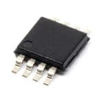
| 描述 | IC DAC NANO 12BIT 8-MSOP数模转换器- DAC IC 5V 12-Bit SPI Interface |
| 产品分类 | |
| 品牌 | Analog Devices |
| 产品手册 | |
| 产品图片 |
|
| rohs | 符合RoHS无铅 / 符合限制有害物质指令(RoHS)规范要求 |
| 产品系列 | 数据转换器IC,数模转换器- DAC,Analog Devices AD5626BRMZnanoDAC™ |
| 数据手册 | |
| 产品型号 | AD5626BRMZ |
| 产品培训模块 | http://www.digikey.cn/PTM/IndividualPTM.page?site=cn&lang=zhs&ptm=19145http://www.digikey.cn/PTM/IndividualPTM.page?site=cn&lang=zhs&ptm=18614http://www.digikey.cn/PTM/IndividualPTM.page?site=cn&lang=zhs&ptm=26125http://www.digikey.cn/PTM/IndividualPTM.page?site=cn&lang=zhs&ptm=26140http://www.digikey.cn/PTM/IndividualPTM.page?site=cn&lang=zhs&ptm=26150http://www.digikey.cn/PTM/IndividualPTM.page?site=cn&lang=zhs&ptm=26147 |
| 产品种类 | 数模转换器- DAC |
| 位数 | 12 |
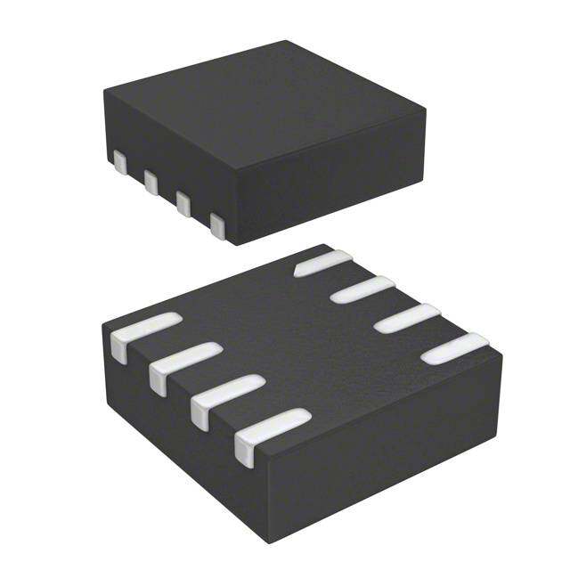
| 供应商器件封装 | 8-MSOP |
| 分辨率 | 12 bit |
| 包装 | 管件 |
| 商标 | Analog Devices |
| 安装类型 | 表面贴装 |
| 安装风格 | SMD/SMT |
| 封装 | Tube |
| 封装/外壳 | 8-TSSOP,8-MSOP(0.118",3.00mm 宽) |
| 封装/箱体 | MSOP-8 |
| 工作温度 | -40°C ~ 85°C |
| 工厂包装数量 | 50 |
| 建立时间 | 16µs |
| 接口类型 | SPI |
| 数据接口 | 串行 |
| 最大功率耗散 | 12.5 mW |
| 最大工作温度 | + 85 C |
| 最小工作温度 | - 40 C |
| 标准包装 | 50 |
| 电压参考 | Internal |
| 电压源 | 单电源 |
| 电源电压-最大 | 5.25 V |
| 电源电压-最小 | 4.75 V |
| 积分非线性 | +/- 1 LSB |
| 稳定时间 | 16 us |
| 系列 | AD5626 |
| 结构 | R-2R |
| 转换器数 | 1 |
| 转换器数量 | 1 |
| 输出数和类型 | 1 电压,单极1 电压,双极 |
| 输出类型 | Voltage |
| 采样比 | 2 MSPs |
| 采样率(每秒) | * |


- 商务部:美国ITC正式对集成电路等产品启动337调查
- 曝三星4nm工艺存在良率问题 高通将骁龙8 Gen1或转产台积电
- 太阳诱电将投资9.5亿元在常州建新厂生产MLCC 预计2023年完工
- 英特尔发布欧洲新工厂建设计划 深化IDM 2.0 战略
- 台积电先进制程称霸业界 有大客户加持明年业绩稳了
- 达到5530亿美元!SIA预计今年全球半导体销售额将创下新高
- 英特尔拟将自动驾驶子公司Mobileye上市 估值或超500亿美元
- 三星加码芯片和SET,合并消费电子和移动部门,撤换高东真等 CEO
- 三星电子宣布重大人事变动 还合并消费电子和移动部门
- 海关总署:前11个月进口集成电路产品价值2.52万亿元 增长14.8%


PDF Datasheet 数据手册内容提取
5 V, 12-Bit nanoDAC, Serial Interface in MSOP and LFCSP Packages AD5626 FEATURES GENERAL DESCRIPTION 8-lead MSOP and 8-lead LFCSP packages The AD5626, a member of the nanoDAC® family, is a complete Complete voltage output with internal reference serial input, 12-bit, voltage output digital-to-analog converter 1 mV/bit with 4.095 V full scale (DAC) designed to operate from a single 5 V supply. It contains 5 V single-supply operation the DAC, input shift register and latches, reference, and a rail- No external components required to-rail output amplifier. The AD5626 monolithic DAC offers 3-wire serial interface, 20 MHz data loading rate the user low cost and ease of use in 5 V only systems. Low power: 2.5 mW Coding for the AD5626 is natural binary with the MSB loaded APPLICATIONS first. The output op amp can swing to either rail and is set to a range of 0 V to 4.095 V for a one-millivolt-per-bit resolution. It Portable instrumentation is capable of sinking and sourcing 5 mA. An on-chip reference Digitally controlled calibration is laser trimmed to provide an accurate full-scale output voltage Servo controls of 4.095 V. Process control equipment PC peripherals This part features a serial interface that is high speed, three- wire, DSP compatible with data in (SDIN), clock (SCLK), and load strobe (LDAC). There is also a chip-select pin for connecting multiple DACs. The CLR input sets the output to zero scale at power on or upon user demand. The AD5626 is specified over the extended industrial tempera- ture range (–40°C to +85°C). The AD5626 is available in MSOP and LFCSP surface-mount packages. FUNCTIONAL BLOCK DIAGRAM VDD AD5626 REF LDAC OUTPUT DAC REGISTER 12-BIT DAC BUFFER VOUT CLR INPUT REGISTER CS SCLK SDIN GND 06757-001 Figure 1. Rev. A Information furnished by Analog Devices is believed to be accurate and reliable. However, no responsibility is assumed by Analog Devices for its use, nor for any infringements of patents or other One Technology Way, P.O. Box 9106, Norwood, MA 02062-9106, U.S.A. rights of third parties that may result from its use. Specifications subject to change without notice. No license is granted by implication or otherwise under any patent or patent rights of Analog Devices. Tel: 781.329.4700 www.analog.com Trademarks and registered trademarks are the property of their respective owners. Fax: 781.461.3113 ©2007—2009 Analog Devices, Inc. All rights reserved.
AD5626 TABLE OF CONTENTS Features .............................................................................................. 1 Output Section ............................................................................ 10 Applications ....................................................................................... 1 Power Supply ............................................................................... 10 General Description ......................................................................... 1 Timing and Control ................................................................... 11 Functional Block Diagram .............................................................. 1 Applications Information .............................................................. 12 Revision History ............................................................................... 2 Power Supplies, Bypassing, and Grounding ........................... 12 Specifications ..................................................................................... 3 Unipolar Output Operation ...................................................... 12 Electrical Characteristics ............................................................. 3 Operating the AD5626 on 12 V or 15 V Supplies Only ........ 13 Timing Characteristics ................................................................ 4 Measuring Offset Error ............................................................. 13 Absolute Maximum Ratings ............................................................ 5 Bipolar Output Operation ......................................................... 13 ESD Caution .................................................................................. 5 Generating a Negative Supply Voltage .................................... 15 Pin Configurations and Function Descriptions ........................... 6 A Single-Supply, Programmable Current Source .................. 15 Typical Performance Characteristics ............................................. 7 Galvanically-Isolated Interface ................................................. 15 Theory of Operation ...................................................................... 10 Microprocessor Interfacing ....................................................... 16 DAC Section ................................................................................ 10 Outline Dimensions ....................................................................... 17 Amplifier Section........................................................................ 10 Ordering Guide .......................................................................... 17 REVISION HISTORY 1/09—Rev. 0 to Rev. A Change to Full-Scale Tempco Paramter and Full-Scale Voltage (Min) Parameter ................................................................. 3 12/07—Revision 0: Initial Version Rev. A | Page 2 of 20
AD5626 SPECIFICATIONS ELECTRICAL CHARACTERISTICS @ V = 5.0 V ± 5%, −40°C ≤ T ≤ +85°C, B grade device, unless otherwise noted. DD A Table 1. Parameter Symbol Condition Min Typ Max Unit STATIC PERFORMANCE Resolution N 12 Bits Relative Accuracy INL −1 ±1/4 +1 LSB Differential Nonlinearity DNL No missing codes −1 ±3/4 +1 LSB Zero-Scale Error V Data = 0x000 1/2 3 LSB ZSE Full-Scale Voltage V Data = 0xFFF1 4.079 4.095 4.111 V FS Full-Scale Tempco2, 3 TCV 20 ppm/°C FS ANALOG OUTPUT Output Current I Data = 0x800 ±5 ±7 mA OUT Load Regulation at Midscale L R = 402 Ω to ∞, data = 0x800 1 3 LSB REG L Capacitive Load C No oscillation2 500 pF L LOGIC INPUTS Logic Input Low Voltage V 0.8 V IL High Voltage V 2.4 V IH Input Leakage Current I 10 μA IL Input Capacitance C 10 pF IL AC CHARACTERISTICS2 Voltage Output Settling Time t To ±1 LSB of final value3 16 μs S DAC Glitch 15 nV-s Digital Feedthrough 15 nV-s SUPPLY CHARACTERISTICS Positive Supply Current I V = 2.4 V, V = 0.8 V, no load 1.5 2.5 mA DD IH IL V = 5 V, V = 0 V, no load 0.5 1 mA DD IL Power Dissipation P V = 2.4 V, V = 0.8 V, no load 7.5 12.5 mW DISS IH IL V = 5 V, V = 0 V, no load 2.5 5 mW DD IL Power Supply Sensitivity PSS ΔV = ±5% 0.002 0.004 %/% DD 1 Includes internal voltage reference error. 2 These parameters are guaranteed by design and not subject to production testing. 3 The settling time specification does not apply for negative going transitions within the last 6 LSBs of ground. Some devices exhibit double the typical settling time in this 6 LSB region. Rev. A | Page 3 of 20
AD5626 TIMING CHARACTERISTICS @ V = 5.0 V ± 5%, −40°C ≤ T ≤ +85°C, unless otherwise noted. DD A Table 2. Parameter1, 2 Limit at T , T Unit Description MIN MAX t 30 ns min Clock width high CH t 30 ns min Clock width low CL t 20 ns min Load pulse width LDW t 15 ns min Data setup DS t 15 ns min Data hold DH t 30 ns min Clear pulse width CLRW t 15 ns min Load setup LD1 t 10 ns min Load hold LD2 t 30 ns min Select CSS t 20 ns min Deselect CSH 1 These parameters are guaranteed by design and not subject to production testing. 2 All input control signals are specified with tr = tf = 5 ns (10% to 90% of 5 V) and timed from a voltage level of 1.6 V. Timing Diagram SDIN D11 D10 D9 D8 D7 D6 D5 D4 D3 D2 D1 DO SCLK tCSS tCSH CS t t LD1 LD2 LDAC SDIN t t DS DH t SCLK CL t CH t LDW LDAC t CLRW CLR t S FS VOUT ZS ±E1R RLSOBR BAND tS 06757-002 Figure 2. Timing Diagram Rev. A | Page 4 of 20
AD5626 ABSOLUTE MAXIMUM RATINGS Stresses above those listed under Absolute Maximum Ratings Table 3. may cause permanent damage to the device. This is a stress Parameter Rating rating only; functional operation of the device at these or any V to GND −0.3 V to +10 V DD other conditions above those indicated in the operational Logic Inputs to GND −0.3 V to V + 0.3 V DD section of this specification is not implied. Exposure to absolute V to GND −0.3 V to V + 0.3 V OUT DD maximum rating conditions for extended periods may affect I Short Circuit to GND 50 mA OUT device reliability. Package Power Dissipation (T max − T )/θ J A JA Thermal Resistance (θ ) JA 8-Lead MSOP 220°C/W ESD CAUTION 8-Lead LFCSP 62°C/W Maximum Junction Temperature 150°C (T max) J Operating Temperature Range −40°C to +85°C Storage Temperature Range −65°C to +150°C Lead Temperature JEDEC industry standard Soldering J-STD-020 Rev. A | Page 5 of 20
AD5626 PIN CONFIGURATIONS AND FUNCTION DESCRIPTIONS VDD 1 8 VOUT VDD 1 8 VOUT CS 2 AD5626 7 GND CS 2 AD5626 7 GND TOP VIEW SSCDLIKN 34 (NToOt Pto V SIEcWale) 65 CLDLRAC 06757-003 SSCDLIKN 34 (Not to Scale) 65 CLDLRAC 06757-004 Figure 3. 8-Lead MSOP Pin Configuration Figure 4. 8-Lead LFCSP Pin Configuration Table 4. Pin Function Descriptions Pin No. Mnemonic Description 1 V Positive Supply. Nominal value 5 V ± 5%. DD 2 CS Chip Select. Active low input. 3 SCLK Clock Input. Clock input for the internal serial input shift register. 4 SDIN Serial Data Input. Data on this pin is clocked into the internal serial register on positive clock edges of the SCLK pin. The most significant bit (MSB) is loaded first. 5 LDAC Serial Register Data Write to DAC Register. Active low input that writes the serial register data into the DAC register. Asynchronous input. 6 CLR Clear DAC Register. Active low digital input that clears the DAC register to zero, setting the DAC to minimum scale. Asynchronous input. 7 GND Ground. Analog ground for the DAC. This also serves as the digital logic ground reference voltage. 8 V Voltage Output from the DAC. Fixed output voltage range of 0 V to 4.095 V with 1 mV/LSB. An internal OUT temperature stabilized reference maintains a fixed full-scale voltage independent of time, temperature, and power supply variations. Table 5. Control Logic Truth Table1 CS2, 3 CLK2 CLR LD4 Serial Shift Register Function DAC Register Function H X H H No effect Latched L L H H No effect Latched L H H H No effect Latched L ↑+ H H Shift-register-data advanced one bit Latched ↑+ L H H Shift-register-data advanced one bit Latched H X H ↓– No effect Updated with current shift register contents H X H L No effect Transparent H X L X No effect Loaded with all zeros H X ↑+ H No effect Latched all zeros 1 ↑+ indicates a positive logic transition; ↓– indicates a negative logic transition; X = don’t care. 2 CS and CLK are interchangeable. 3 Returning CS high avoids an additional false clock of serial data input. 4 Do not clock in serial data while LD is low. Rev. A | Page 6 of 20
AD5626 TYPICAL PERFORMANCE CHARACTERISTICS 5 VDD = 5V TA = 25°C 4 RL TIED TO AGND E (V) DATA = 0xFFF AG 3 T L O 1 V T U 2 P T U O 1 0 DRAL TTAIE =D 0TxO00 50V 06757-005 06757-008 10 100 1k 10k 100k CH1 5.00V CH2 100mV M2.00ms A CH1 210µV LOAD RESISTANCE (Ω) Figure 5. Output Voltage vs. Load Figure 8. Broadband Noise 100 1.2 +85°C +25°C 1.1 E (mV) 10 –40°C 1.0 TAG 1 mA) 0.9 VOL NT ( 0.8 N RE W 0.1 R 0.7 O U D C LL- LY 0.6 UT PU 0.01 SUPP 0.5 TP 0.4 U0.001 O 0.0001 06757-006 00..32 06757-009 1 10 100 1000 0 0.5 1.0 1.5 2.0 2.5 3.0 3.5 4.0 4.5 5.0 OUTPUT SINK CURRENT (µA) LOGIC VOLTAGE VALUE (V) Figure 6. Output Pull-Down Voltage vs. Output Sink Current Capability Figure 9. Supply Current vs. Logic Input Voltage 80 80 70 60 B) d 60 T (mA) 40 CTION ( 50 N E URRE 20 Y REJ 40 OUTPUT C –200 ER SUPPL 3200 W 10 O P –40 –60 06757-007 –100 06757-010 0 0.5 1.0 1.5 2.0 2.5 3.0 3.5 4.0 4.5 5.0 10 100 1k 10k 100k OUTPUT VOLTAGE (V) FREQUENCY (Hz) Figure 7. Short-Circuit Current Figure 10. Power Supply Rejection vs. Frequency Rev. A | Page 7 of 20
AD5626 5.0 ΔVFS ≤ 1 LSB DATA = 0xFFF TA = 25°C 4.8 LDAC 1 V) 4.6 N ( MI V DD 4.4 PROPER OPERATION WHEN VDD SUPPLY VOLTAGE IS ABOVE CURVE 44..02 06757-011 SOURCE VERTICLE SCALE OFFSET HORIZONTAL SCALOEUTPPOUTSIT2ION06757-014 0.01 0.1 1 10 CH1 2.00V/DIV –1.95V 5.0µs/DIV 22.725µs OUTPUT LOAD CURRENT (mA) CH2 200mV/DIV 3.9875mV 5.0µs/DIV 22.725µs Figure 11. Minimum Supply Voltage vs. Load Figure 14. Rise Time Detail 2.11 0x7FF 0x800 2.10 0x800 0x7FF 2.09 LDAC 1 2.08 V) (UT 2.07 OUTPUT 2 O V 2.06 2.05 22..0043 06757-012 SOURCE VERTICLE SCALE OFFSET HORIZONTAL SCALE POSITIO06757-015N 0 0.5 1.0 1.5 2.0 2.5 3.0 3.5 4.0 CH1 2.00V/DIV –1.95V 5.0µs/DIV 22.725µs TIME (ns) CH2 200mV/DIV 87.6mV 5.0µs/DIV 22.725µs Figure 12. Midscale DAC Glitch Performance Figure 15. Fall Time Detail 0.20 +85°C +25°C 0.15 –40°C 0.10 B) 0.05 S L L ( N 0 I –0.05 2 OUTPUT 06757-013 ––00..1150 VDD = 5V 06757-016 SOURCE VERTICLE SCALE OFFSET HORIZONTAL SCALE POSITION 0 500 1000 1500 2000 2500 3000 3500 4000 CH2 1.00V/DIV 2.90V 50.0µs/DIV 105.758µs CODE Figure 13. Large Signal Settling Time Figure 16. Integral Linearity Error vs. Digital Code Rev. A | Page 8 of 20
AD5626 60 10 TUE = ΣINL + ZS + FS SS = 300 UNITS VDD = 5V 50 TA = 25°C √Hz) NDAOT LAO =A 0DxFFF V/ NITS 40 TY (µ 1 F U NSI O E ER 30 E D B S M OI U N NN 20 UT 0.1 P T U 10 O 0 06757-017 0.01 06757-020 –12 –8 –4 0 4 8 12 10 100 1k 10k 100k TOTAL UNADJUSTED ERROR (mV) FREQUENCY (Hz) Figure 17. Total Unadjusted Error Histogram Figure 20. Output Voltage Noise vs. Frequency 4.115 5 4.110 NVDOD L =O 5AVD 4 135 UNITS TESTED SS = 300 UNITS mV) 3 UTPUT (V)44..110050 AVG + 3σ CHANGE ( 21 SCALE O44..009950 AVG OLTAGE –10 AVERAGE RANGE ULL- UT V –2 F4.085 AVG – 3σ TP U –3 O 44..007850 06757-018 ––54 RTOEA ZDEIRNOG SH ONOURR MTAIMLEIZ PEODINT 06757-021 –50 –25 0 25 50 75 100 125 0 200 400 600 800 1000 1200 TEMPERATURE (°C) HOURS OF OPERATION AT 125°C Figure 18. Full-Scale Output Voltage vs. Temperature Figure 21. Long-Term Drift Accelerated by Burn-In 0.50 1.6 VDD = 4.75V 0.45 1.4 VVDDDD == 55.V25V 0.40 1.2 E (mV)00..3350 ENT (mA) 1.0 L R CA0.25 UR 0.8 S C O 0.20 Y R L 0.6 E P Z0.15 UP S 0.4 0.10 0.050 06757-019 0.02 06757-022 –40 –20 0 20 40 60 80 –40 –20 0 20 40 60 80 TEMPERATURE (°C) TEMPERATURE (°C) Figure 19. Zero-Scale Voltage vs. Temperature Figure 22. Supply Current vs. Temperature Rev. A | Page 9 of 20
AD5626 THEORY OF OPERATION The AD5626 is a complete, ready-to-use, 12-bit digital-to-analog VDD converter (DAC). It contains a voltage-switched, 12-bit, laser- P-CH trimmed DAC, a curvature-corrected band gap reference, a rail-to-rail output op amp, a DAC register, and a serial data input register. The serial data interface consists of an SCLK, VOUT serial data in (SDIN), and a load strobe (LDAC). This basic N-CH 3-wire interface offers maximum flexibility for interface to the widest variety of serial data input loading requirements. In aanddd iati poonw, ae rC-oSn s-erleescett iCs LpRro pviind etod sfiomr pmliufylt isptaler tp oarc kpaegriinogd ilco raedsientgs. AGND 06757-024 Figure 24. Equivalent Analog Output Circuit DAC SECTION Figure 24 shows an equivalent output schematic of the rail-to- The DAC is a 12-bit voltage mode device with an output that rail amplifier with its N-channel pull-down FETs that pull an swings from the GND potential to the 2.5 V internal band gap output load directly to GND. The output sourcing current is voltage. It uses a laser trimmed, rail-to-rail ladder which is provided by a P-channel pull-up device that can supply GND switched by N-channel MOSFETs. The output voltage of the terminated loads, especially at the low supply tolerance values DAC has a constant resistance independent of digital input of 4.75 V. Figure 5 and Figure 6 provide information on output code. The DAC output internally connects to the rail-to-rail swing performance near ground and full-scale as a function of output op amp. load. In addition to resistive load driving capability, the amplifier AMPLIFIER SECTION has also been carefully designed and characterized for up to 500 pF capacitive load driving capability. A low power consumption, precision amplifier buffers the DAC output. This amplifier contains a differential PNP pair input POWER SUPPLY stage that provides low offset voltage and low noise, as well as The very low power consumption of the AD5626 is a direct the ability to amplify the zero-scale DAC output voltages. result of a circuit design optimizing use of the CBCMOS process. The rail-to-rail amplifier is configured with a gain of 1.6384 By using the low power characteristics of the CMOS for the (= 4.095 V/2.5 V) to set the 4.095 V full-scale output (1 mV/LSB). logic, and the low noise, tight matching of the complementary See Figure 23 for an equivalent circuit schematic of the analog bipolar transistors, good analog accuracy is achieved. section. For power consumption sensitive applications, it is important VOLTAGE SWITCHED 12-BIT to note that the internal power consumption of the AD5626 RAIL-TO-RAIL CONVERTER RAIL-TO-RAIL BAND GAP OUTPUT is strongly dependent on the actual logic input voltage levels REFERENCE 2R AMPLIFIER present on the SDIN, CS, LDAC, and CLR pins. Because these inputs are standard CMOS logic structures, they contribute BUFFER R VOUT R2 static power dissipation dependent on the actual driving 2R R1 Logic VOH and Logic VOL voltage levels. The graph in Figure 9 2.5V shows the effect on total AD5626 supply current as a function R 2R AV = 1.638 of the actual value of input logic voltage. Consequently, use of (= 4.095V/2.5V) CMOS logic vs. TTL minimizes power dissipation in the static state. A V = 0 V on the SDIN, CS, and CLR pins provides the IL SPDT 2R lowest standby power dissipation of 2.5 mW (500 μA × 5 V). N-CHANNEL FET SWITCHES 2R 06757-023 Aposw weirt hs uapnpyl ya nbael obgy psyasstseemd ,o int itsh ree scaommem PeCn dceadrd t hthaat tt hcoe nAtaDin5s6 26 Figure 23. Equivalent AD5626 Schematic of Analog Section the chip. Figure 10 shows the power supply rejection vs. frequency performance. This should be taken into account when using higher The op amp has a 16 μs typical settling time to 0.01%. There are frequency, switched mode power supplies with ripple frequencies slight differences in settling time for negative slewing signals vs. of 100 kHz and higher. positive slewing signals. See the oscilloscope photos in the Typical Performance Characteristics section of this data sheet. One advantage of the rail-to-rail output amplifier used in the AD5626 is the wide range of usable supply voltage. The part is OUTPUT SECTION fully specified and tested over temperature for operation from The rail-to-rail output stage of this amplifier is designed to 4.75 V to 5.25 V. If reduced linearity and source current capa- provide precision performance when operating near either bility near full scale can be tolerated, operation of the AD5626 power supply. is possible down to 4.3 V. The minimum operating supply Rev. A | Page 10 of 20
AD5626 voltage vs. load current plot, shown in Figure 11, provides register by strobing the LDAC pin. The DAC register uses a information for operation below VDD = 4.75 V. level sensitive LDAC strobe that should be returned high before TIMING AND CONTROL any new data is loaded into the serial input register. At any time, the contents of the DAC register can be reset to zero by strobing The AD5626 has a separate serial input register from the the CLR pin that causes the DAC output voltage to go to zero 12-bit DAC register that allows preloading of a new data value volts. Figure 2 details all of the timing requirements together into the serial register without disturbing the present DAC with Table 5, the control logic truth table. output voltage. After the new value is fully loaded in the serial input register, it can be asynchronously transferred to the DAC Rev. A | Page 11 of 20
AD5626 APPLICATIONS INFORMATION POWER SUPPLIES, BYPASSING, AND GROUNDING for the internal voltage reference and the output amplifier. Therefore, to minimize errors, connect the ground connection All precision converter products require careful application of of the AD5626 to a high quality analog ground, such as the one good grounding practices to maintain full rated performance. previously described. Generous bypassing of the DACs supply Because the AD5626 has been designed for 5 V applications, it effectively reduces supply line induced errors. Local supply is ideal for those applications under microprocessor or micro- bypassing consisting of a 10 μF tantalum electrolytic capacitor computer control. In these applications, digital noise is prevalent; in parallel with a 0.1 μF ceramic capacitor is recommended. therefore, special care must be taken to ensure that its inherent Connect the decoupling capacitors between the DAC supply precision is maintained by exercising particularly good engineering pin (Pin 1) and the analog ground (Pin 7). judgment when addressing the power supply, grounding, and bypassing issues using the AD5626. Figure 26 shows how the ground and bypass connections should be made to the AD5626. Use a well-filtered and regulated power supply for the AD5626. The device has been completely characterized for a 5 V supply 5V with a tolerance of ±5%. Because a 5 V logic supply is almost universally available, it is not recommended to connect the 1 DAC directly to an unfiltered logic supply without careful CS 2 VDD +10µF 0.1µF filtering. Tapping a logic circuit supply for the DAC supply CLR 6 AD5626 is unwise because fast logic with nanosecond transition edges LDAC 5 VOUT 8 VOUT induce high current pulses. The high transient current pulses SCLK 3 can generate glitches hundreds of millivolts in amplitude due SDIN 4 to wiring resistances and inductances. This high frequency GND 7 noise corrupts the analog circuits internal to the DAC and cEavuesne sth eorurogrhs .t heir spike noise is lower in amplitude, directly TO ANALOG GROUND 06757-026 Figure 26. Recommended Grounding and Bypassing Scheme for the AD5626 tapping the output of a 5 V system supply can cause errors UNIPOLAR OUTPUT OPERATION because these supplies are of the switching regulator type that can and do generate a great deal of high frequency noise. There- This is the basic mode of operation for the AD5626. As shown fore, power the DAC and any associated analog circuitry directly in Figure 27, the AD5626 is designed to drive loads as low as from the system power supply outputs using appropriate filtering. 2 kΩ in parallel with 500 pF. The code table for this operation is provided in Table 6. Figure 25 illustrates how a clean, analog-grade supply can be generated from a 5 V logic supply using a differential LC filter 5V 10µF with separate power supply and return lines. With the values + 0.1µF shown, this filter can easily handle 100 mA of load current without saturating the ferrite cores. Higher current capacity 1 can be achieved with larger ferrite cores. For lowest noise, all CS 2 VDD electrolytic capacitors should be of the low equivalent series CLR 6 AD5626 resistance (ESR) type. 0V ≤ VOUT ≤ 4.095V LDAC 5 VOUT 8 2kΩ 500pF FERRITE BEADS: SCLK 3 TTL/CMOS 2 TURNS CILROCGUIICTS +5V SDIN 4 GND +1E0L0EµCFT. +1T0A-N20Tµ.F 0C.E1µRF. 7 06757-027 +5V Figure 27. Unipolar Output Operation RETURN POWER5 VSUPPLY 06757-025 THaebxaled 6e.c Uimnaipl Noluamr Cbeord e TDabelcei mal Number Analog Output Figure 25. Properly Filtering a 5 V Logic Supply Yields a High Quality in DAC Register in DAC Register Voltage (V) Analog Supply FFF 4095 4.095 To fit the AD5626 in an 8-lead package, only one ground 801 2049 2.049 connection to the device is accommodated. The ground 800 2048 2.048 connection of the DAC serves as the return path for supply 7FF 2047 2.047 currents as well as the reference point for the digital input 000 0 0 thresholds. The ground connection also serves as the supply rail Rev. A | Page 12 of 20
AD5626 OPERATING THE AD5626 ON 12 V OR 15 V specified to be ±3 LSBs. Because zero scale coincides with zero SUPPLIES ONLY volt, it is not possible to measure negative offset error. Although the AD5626 has been specified to operate on a single, 5V 0.1µF 5 V supply, a single 5 V supply may not be available in many applications. Because the AD5626 consumes no more than 2.5 mA 1 maximum, an integrated voltage reference, such as the ADR02, CS 2 VDD can be used as the 5 V supply for the AD5626. See Figure 28 for CLR 6 AD5626 the circuit configuration. Notice that the output voltage of the LDAC 5 VOUT 8 VOUT reference requires no trimming because of the excellent load SCLK 3 R 200µA, MAX regulation and tight initial output voltage tolerance of the ADR02. SDIN 4 Although the maximum supply current of the AD5626 is 2.5 mA, GND 7 V– local bypassing of the ADR02 output with at least 0.1 μF at the DAC voltage supply pin is recommended to prevent the internal dreifgeirtaeln ccier couf itths eo Df tAhCe .D AC from affecting the internal voltage SET CODE = 0x000 AND MEASURE VOUT 06757-029 Figure 29. Measuring Zero-Scale or Offset Error 12V OR 15V 1µF By adding a pull-down resistor from the output of the AD5626 to a negative supply as shown in Figure 29, offset errors can be 2 read at zero code. This configuration forces the output P-channel ADR02 6 MOSFET to source current to the negative supply thereby allowing 0.1µF 4 the designer to determine in which direction the offset error 1 appears. The value of the resistor should be such that, at zero CS 2 VDD code, current through the resistor is 200 μA, maximum. CLR 6 AD5626 BIPOLAR OUTPUT OPERATION LDAC 5 8 VOUT Although the AD5626 has been designed for single-supply SCLK 3 operation, bipolar operation is achievable using the circuit SDIN 4 GND illustrated in Figure 30. The circuit uses a single-supply, rail- 7 06757-028 troef-erraeiln OceP r2e9q5u oirpe da mtop l eavnedl sthheif tR tEhFe0 D3A toC g oeuntepruatt ev tohltea −ge2.. 5 V Figure 28. Operating the AD5626 on 12 V or 15 V Supplies Using an Note that the −2.5 V reference is generated without the use of ADR02 Voltage Reference precision resistors. The circuit configuration provides an output MEASURING OFFSET ERROR voltage in the range of −5 V ≤ V ≤ +5 V and is coded in comple- OUT One of the most commonly specified endpoint errors associated mentary offset binary. Although each DAC LSB corresponds to with real world nonideal DACs is offset error. In most DAC 1 mV, each output LSB has been scaled to 2.44 mV. Table 7 lists testing, the offset error is measured by applying the zero-scale the relationship between the digital codes and output voltage. code and measuring the output deviation from 0 V. The transfer function of the circuit is given by There are some DACs where offset errors are present but not R4 R4 V =−1mV×DigitalCode× +2.5× observable at the zero scale because of other circuit limitations O R1 R2 (for example, zero coinciding with single-supply ground). In and, for the circuit values shown, becomes these DACs, nonzero output at zero code cannot be read as the V = −2.44 mV × Digital Code + 5 V offset error. In the AD5626, for example, the zero-scale error is O Rev. A | Page 13 of 20
AD5626 +5V 0.1µF FULL-SCALE ADJUST 10µF + R4 23.7kΩ 1 P3 CS 2 VDD 500Ω +5V CLR 6 AD5626 R1 10kΩ LDAC 5 VOUT 8 6 – 8 SCLK 3 R2 R2437kΩ A2 7 SDIN 4 12.7kΩ 5 + 4 –5V ≤ VO≤ +5V GND 7 P2 –5V –2.5V 10kΩ ZERO-SCALE ADJUST +5V 0.01µF 0.1µF 2.5V 2 TRIM 100Ω 6 2 – ADR03 A1 1 –2.5V P1 5 10kΩ 3 + 4 A1, A2 = 1/2 OP295 06757-030 Figure 30. Bipolar Output Operation +5V 0.1µF 2 R1 R2 ADR03 6 +2.5V 4 +5V +5V 0.1µF 2 – 8 1 A1 1 VO CS 2 VDD 3 + 4 CLR 6 AD5626 R3 –5V LDAC 5 VOUT 8 SCLK 3 R4 SDIN 4 A1 = 1/2 OP295 GND 7 VOUTRANGE R1 R2 R3 R4 ±±25.5VV 1100kkΩΩ 1200kkΩΩ 1100kkΩΩ 4135.2kkΩΩ + + 2 47949ΩΩ 06757-031 Figure 31. Bipolar Output Operation Without Trim Table 7. Bipolar Code matching. Mismatching between R1 and R2 causes offset and gain errors whereas an R4 to R1 or R4 to R2 mismatch yields Hexadecimal Number Decimal Number Analog Output in DAC Register in DAC Register Voltage (V) gain errors. FFF 4095 −4.9976 For applications that do not require high accuracy, the circuit 801 2049 −2.44E − 3 illustrated in Figure 31 can also be used to generate a bipolar 800 2048 0 output voltage. In this circuit, only one op amp is used and no 7FF 2047 +2.44E − 3 potentiometers are used for offset and gain trim. The output 000 0 +5 voltage is coded in offset binary and is given by To maintain monotonicity and accuracy, R1, R2, and R4 should ⎛ R4 ⎞ ⎛ R2⎞ R2 V =1mV×DigitalCode×⎜ ⎟×⎜1+ ⎟−2.5× be selected to match within 0.01% and must all be of the same O ⎝R3+R4⎠ ⎝ R1⎠ R1 (preferably metal foil) type to assure temperature coefficient Rev. A | Page 14 of 20
AD5626 For the ±2.5 V output range and the circuit values shown in the 5V 0.1µF table in Figure 31, the transfer equation becomes VS V = 1.22 mV × Digital Code − 2.5 V 1 O CS 2 VDD LOAD Similarly, for the 5 V output range, the transfer equation +5V CLR 6 AD5626 becomes LDAC 5 VOUT 8 3 + VO = 2.44 mV × Digital Code − 5 V SCLK 3 A1 1 2N2222 2 – GENERATING A NEGATIVE SUPPLY VOLTAGE SDIN 4 GND 7 Some applications may require bipolar output configuration but only have a single power supply rail available. This is very A1 = 1/2 OP295 R1 4.02kΩ common in data acquisition systems using microprocessor- P1 based systems. In these systems, only 12 V, 15 V, and/or 5 V 200Ω are available. FAUDLJLU-SSTCALE 06757-033 Figure 32 shows a method for generating a negative supply Figure 33. A Single-Supply, Programmable Current Source voltage using one CD4049, a CMOS hexadecimal inverter, and The usable output voltage range of the current sink is 5 V to operating on 12 V or 15 V. The circuit is essentially a charge 60 V. The low limit of the range is controlled by transistor pump where two of the six inverters are used as an oscillator. saturation, and the high limit is controlled by the collector-base For the values shown, the frequency of oscillation is approx- breakdown voltage of the 2N2222. imately 3.5 kHz and is fairly insensitive to supply voltage GALVANICALLY-ISOLATED INTERFACE because R1 > 2 × R2. In many process control type applications, it is necessary to The remaining four inverters are wired in parallel for higher provide an isolation barrier between the controller and the unit output current. The square wave output is level translated by C2 being controlled to protect and isolate the controlling circuitry to a negative-going signal rectified using a pair of 1N4001s, and from any hazardous common-mode voltages that may occur. then filtered by C3. With the values shown, the charge pump An iCoupler® can provide isolation in excess of 2.5 kV. The provides an output voltage of −5 V for currents loading in the serial loading structure of the AD5626 makes it ideal for range 0.5 mA ≤ I ≤ 10 mA with a 15 V supply and 0.5 mA ≤ OUT isolated interfaces as the number of interface lines is kept to I ≤ 7 mA with a 12 V supply. OUT a minimum. Figure 34 illustrates a 4-channel isolated interface 7 6 using an ADuM1400. For further information, visit INVERTERS = CD4049 http://www.analog.com/icouplers. 9 10 C2 D2 R3 47µF 1N4001 470Ω 3 2 5 4 + –5V MICROCONTROLLER ADuM1400* R5110kΩ R5.210k.Ω0C21µF 1114 1125 D1N14001 + C473µF 15ZN.E15NV2E3R1 06757-032 SESREIRAILA LC LDOACTKA OOUUTT VVIIAB EENNCCOODDEE DDEECCOODDEE VVOOAB TTOO SSCDLINK Figure 32. Generating a –5 V Supply When Only 12 V or 15 V Is Available SYNC OUT VIC ENCODE DECODE VOC TO SYNC A SINGLE-SUPPLY, PROGRAMMABLE CONTROL OUT VID ENCODE DECODE VOD TO LDAC CThUeR cRircEuNitT in S FOigUuRreC 3E3 shows how the AD5626 can be used *ADDITIONAL PINS OMITTED FOR CLARITY. 06757-034 with an OP295 single-supply, rail-to-rail, output op amp to Figure 34. An iCoupler-Isolated DAC Interface provide a digitally programmable current sink from V SOURCE that consumes less than 3.8 mA, maximum. The DAC output voltage is applied across R1 by placing the 2N2222 transistor in the feedback loop of the OP295. For the circuit values shown, the full-scale output current is 1 mA, which is given by the following equation: DW×4.095V I = OUT R1 where DW = the binary digital input code of the AD5626. Rev. A | Page 15 of 20
AD5626 MICROPROCESSOR INTERFACING data is then transferred serially to the AD5626. During the AD5626 to MC68HC11 Interface second byte load, the first 4 MSBs of the first byte are pushed out of the input shift register of the DAC. At the end of the The circuit illustrated in Figure 35 shows a serial interface second byte load, PC0 is taken high. To prevent accidental between the AD5626 and the MC68HC11 8-bit microcontroller. advancing of the internal shift register, SCLK must already be SCK of the MC68HC11 drives SCLK of the AD5626, whereas asserted before PC0 is taken high. To transfer the contents of the MOSI output drives the serial data line, SDIN, of the AD5626. the input shift register to the DAC register, PD5 is taken low, The CLR, LDAC, and CS signals of the DAC are derived from asserting the LDAC input. The CLR input of the DAC, controlled the PC1, PD5, and PC0 port lines, respectively, as shown. by the MC68HC11 PC1 port, provides an asynchronous clear For correct operation of the serial interface, configure the function, setting the DAC output to zero. MC68HC11 such that its CPOL bit is set to 1 and its CPHA bit MC68HC11* AD5626 is also set to 1. When the serial data is to be transmitted to the PC1 CLR DAC, PC0 is taken low, asserting the CS input of the DAC. When PC0 CS the MC68HC11 is configured in this manner, serial data on PD5 LDAC MOSI is valid on the rising edge of SCLK. The MC68HC11 SCK SCLK transmits its serial data in 8-bit bytes (MSB first), with only MOSI SDIN ediagthat t roi stihneg i cnlpouctk s eedrigaels r oegccisuterrri onfg t ihne tAheD t5r6a2n6sm, PiCt c0y icsl ele. fTto l olowa d *ADDITIONAL PINS OMITTED FOR CLARITY. 06757-035 after the first eight bits are transferred, and a second byte of Figure 35. AD5626 to MC68HC11 Interface Rev. A | Page 16 of 20
AD5626 OUTLINE DIMENSIONS 3.20 3.00 2.80 8 5 5.15 3.20 4.90 3.00 4.65 2.80 1 4 PIN 1 0.65 BSC 0.95 0.85 1.10 MAX 0.75 0.80 0.15 0.38 0.23 8° 0.60 0.00 0.22 0.08 0° 0.40 COPLANARITY SEATING 0.10 PLANE COMPLIANT TO JEDEC STANDARDS MO-187-AA Figure 36. 8-Lead Mini Small Outline Package [MSOP] (RM-8) Dimensions shown in millimeters 0.30 3.00 0.23 0.65 BSC BSC SQ 0.18 5 8 PIN 1 IANRDEEAX EXPPOADSED 11..7644 (BOTTOM VIEW) 0.50 1.49 0.40 0.30 4 1 PIN 1 INDICATOR TOP VIEW 2.48 (R 0.19) 2.38 0.80 MAX 0.80 0.55 NOM 2.23 0.75 0.05 MAX 0.70 0.02 NOM SEATING PLANE 0.20 REF 062507-A Figure 37. 8-Lead Lead Frame Chip Scale Package [LFCSP_WD] 3 mm x 3 mm Body, Very Very Thin, Dual Lead (CP-8-3) Dimensions shown in millimeters ORDERING GUIDE Model INL (LSB) Temperature Range Package Description Package Option Branding AD5626BRMZ1 ±1 –40°C to +85°C 8-Lead MSOP RM-8 DAP AD5626BRMZ-REEL71 ±1 –40°C to +85°C 8-Lead MSOP RM-8 DAP AD5626BCPZ-REEL71 ±1 –40°C to +85°C 8-Lead LFCSP_WD CP-8-3 DAP 1 Z = RoHS Compliant Part. Rev. A | Page 17 of 20
AD5626 NOTES Rev. A | Page 18 of 20
AD5626 NOTES Rev. A | Page 19 of 20
AD5626 NOTES ©2007—2009 Analog Devices, Inc. All rights reserved. Trademarks and registered trademarks are the property of their respective owners. D06757-0-1/09(A) Rev. A | Page 20 of 20
Mouser Electronics Authorized Distributor Click to View Pricing, Inventory, Delivery & Lifecycle Information: A nalog Devices Inc.: AD5626BCPZ-REEL7 AD5626BRMZ AD5626BRMZ-REEL7