ICGOO在线商城 > 集成电路(IC) > 数据采集 - 数模转换器 > AD5383BSTZ-5

 Datasheet下载
- 型号: AD5383BSTZ-5
- 制造商: Analog
- 库位|库存: xxxx|xxxx
- 要求:
| 数量阶梯 | 香港交货 | 国内含税 |
| +xxxx | $xxxx | ¥xxxx |
查看当月历史价格
查看今年历史价格
AD5383BSTZ-5产品简介:
ICGOO电子元器件商城为您提供AD5383BSTZ-5由Analog设计生产,在icgoo商城现货销售,并且可以通过原厂、代理商等渠道进行代购。 AD5383BSTZ-5价格参考。AnalogAD5383BSTZ-5封装/规格:数据采集 - 数模转换器, 12 位 数模转换器 32 100-LQFP(14x14)。您可以下载AD5383BSTZ-5参考资料、Datasheet数据手册功能说明书,资料中有AD5383BSTZ-5 详细功能的应用电路图电压和使用方法及教程。
AD5383BSTZ-5 是由 Analog Devices Inc. 生产的一款高精度、低功耗的数模转换器(DAC),属于数据采集系统中的关键组件。该型号的应用场景广泛,尤其适用于需要高分辨率和稳定输出的工业控制、医疗设备、通信系统及测试测量等领域。

1. 工业自动化与控制系统:AD5383BSTZ-5 可用于各种工业自动化应用中,如过程控制、电机驱动和传感器接口等。它能够将数字信号精确转换为模拟电压或电流,从而实现对温度、压力、流量等物理量的精准控制。其内置的参考电压源和缓冲输出特性,使得该器件在复杂电磁环境中仍能保持良好的性能。

2. 医疗仪器:在医疗成像设备(如超声波机)、监护仪和其他诊断装置中,AD5383BSTZ-5 提供了高精度的信号生成能力,有助于提高图像质量和测量准确性。此外,其低噪声特性和快速建立时间对于确保患者安全至关重要。

3. 通信基础设施:对于无线基站、有线调制解调器以及其他通信设施而言,这款 DAC 能够支持多种通信协议,并且可以处理复杂的调制波形。它的宽带宽和高线性度使其成为构建高性能发射机的理想选择。

4. 测试与测量设备:在精密测试仪器如示波器、频谱分析仪以及自动测试设备 (ATE) 中,AD5383BSTZ-5 的高分辨率和可编程增益功能可以帮助工程师更准确地校准和验证电子电路的工作状态。

总之,AD5383BSTZ-5 凭借其卓越的技术参数,在众多要求严苛的应用场合下表现出色,是现代电子产品设计不可或缺的一部分。
| 参数 | 数值 |
| 产品目录 | 集成电路 (IC)半导体 |
| 描述 | IC DAC 12BIT 32CH 5V 100-LQFP数模转换器- DAC 32-CH 12-Bit IC 6uS |
| 产品分类 | |
| 品牌 | Analog Devices |
| 产品手册 | |
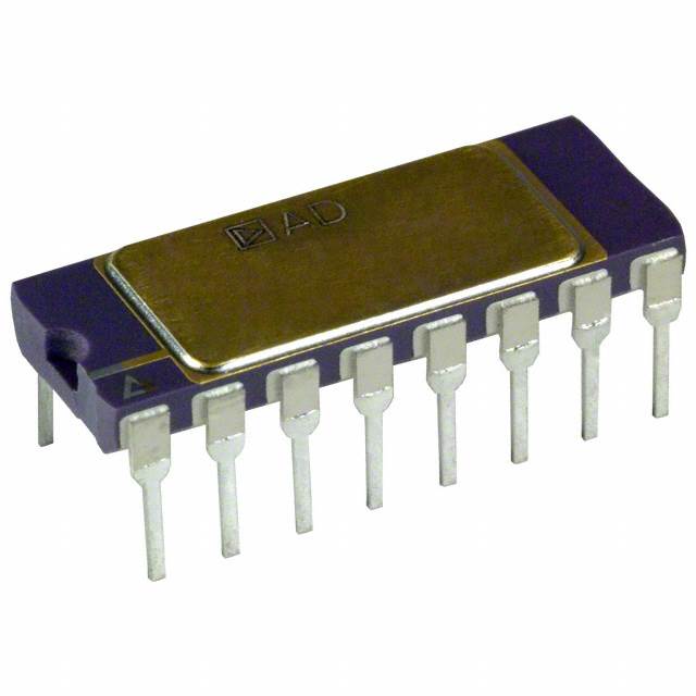
| 产品图片 |
|
| rohs | 符合RoHS无铅 / 符合限制有害物质指令(RoHS)规范要求 |
| 产品系列 | 数据转换器IC,数模转换器- DAC,Analog Devices AD5383BSTZ-5- |
| 数据手册 | |
| 产品型号 | AD5383BSTZ-5 |
| PCN设计/规格 | |
| 产品培训模块 | http://www.digikey.cn/PTM/IndividualPTM.page?site=cn&lang=zhs&ptm=19145http://www.digikey.cn/PTM/IndividualPTM.page?site=cn&lang=zhs&ptm=18614http://www.digikey.cn/PTM/IndividualPTM.page?site=cn&lang=zhs&ptm=26125http://www.digikey.cn/PTM/IndividualPTM.page?site=cn&lang=zhs&ptm=26140http://www.digikey.cn/PTM/IndividualPTM.page?site=cn&lang=zhs&ptm=26150http://www.digikey.cn/PTM/IndividualPTM.page?site=cn&lang=zhs&ptm=26147 |
| 产品种类 | 数模转换器- DAC |
| 位数 | 12 |
| 供应商器件封装 | 100-LQFP(14x14) |
| 其它名称 | AD5383BSTZ5 |
| 分辨率 | 12 bit |
| 包装 | 托盘 |
| 商标 | Analog Devices |
| 安装类型 | 表面贴装 |
| 安装风格 | SMD/SMT |
| 封装 | Tray |
| 封装/外壳 | 100-LQFP |
| 封装/箱体 | LQFP-100 |
| 工作温度 | -40°C ~ 85°C |
| 工厂包装数量 | 90 |
| 建立时间 | 6µs |
| 接口类型 | SPI |
| 数据接口 | 串行,并联 |
| 最大工作温度 | + 85 C |
| 最小工作温度 | - 40 C |
| 标准包装 | 1 |
| 电压参考 | Internal, External |
| 电压源 | 单电源 |
| 电源电压-最大 | 5.5 V |
| 电源电压-最小 | 2.7 V |
| 积分非线性 | +/- 1 LSB |
| 稳定时间 | 6 us |
| 系列 | AD5383 |
| 结构 | Resistor String |
| 设计资源 | |
| 转换器数 | 32 |
| 转换器数量 | 32 |
| 输出数和类型 | 32 电压,单极32 电压,双极 |
| 输出类型 | Voltage |
| 采样比 | 167 kSPs |
| 采样率(每秒) | 167k |


- 商务部:美国ITC正式对集成电路等产品启动337调查
- 曝三星4nm工艺存在良率问题 高通将骁龙8 Gen1或转产台积电
- 太阳诱电将投资9.5亿元在常州建新厂生产MLCC 预计2023年完工
- 英特尔发布欧洲新工厂建设计划 深化IDM 2.0 战略
- 台积电先进制程称霸业界 有大客户加持明年业绩稳了
- 达到5530亿美元!SIA预计今年全球半导体销售额将创下新高
- 英特尔拟将自动驾驶子公司Mobileye上市 估值或超500亿美元
- 三星加码芯片和SET,合并消费电子和移动部门,撤换高东真等 CEO
- 三星电子宣布重大人事变动 还合并消费电子和移动部门
- 海关总署:前11个月进口集成电路产品价值2.52万亿元 增长14.8%


PDF Datasheet 数据手册内容提取
32-Channel, 3 V/5 V, Single-Supply, 12-Bit, denseDAC Data Sheet AD5383 FEATURES INTEGRATED FUNCTIONS Guaranteed monotonic Channel monitor INL error: ±1 LSB max Simultaneous output update via LDAC On-chip 1.25 V/2.5 V, 10 ppm/°C reference Clear function to user-programmable code Temperature range: –40°C to +85°C Amplifier boost mode to optimize slew rate Rail-to-rail output amplifier User programmable offset and gain adjust Power-down mode Toggle mode enables square wave generation Package type: 100-lead LQFP (14 mm × 14 mm) Thermal monitor User Interfaces APPLICATIONS Parallel Serial (SPI®-/QSPI™-/MICROWIRE™-/DSP-compatible, Variable optical attenuators (VOA) featuring data readback) Level setting (ATE) I2C-compatible Optical microelectro-mechanical systems (MEMS) Robust 6.5 kV HBM and 2 kV FICDM ESD rating Control systems Instrumentation FUNCTIONAL BLOCK DIAGRAM DVDD (×3) DGND (×3) AVDD (×4) AGND (×4) DAC GND (×4) REFGND REFOUT/REFIN SIGNAL GND (×4) PD SER/PAR AD5383 1.25V/2.5V REFERENCE FIFO EN CS/(SYNC/AD0) WR/(DCEN/AD1) SDO 12 INPUT 12 12 DAC 12 DAC 0 REG 0 REG 0 VOUT0 DB11/(DIN/SDA) 12 DB10/(SCLK/SCL) m REG 0 DB9/(SPI/I2C) FIFO 12 c REG 0 R DB8 + R INTERFACE STATE CONTROL MACHINE LOGIC + 12 INPUT 12 12 DAC 12 DB0 CONTROL REG 1 REG 1 DAC 1 LOGIC VOUT1 A4 12 m REG 1 VOUT2 A0 12 c REG 1 R VOUT3 R REG 0 VOUT4 REG 1 12 INPUT 12 12 DAC 12 DAC 6 VOUT5 REG 6 REG 6 POWER-ON VOUT6 RESET RESET 12 m REG 6 BUSY 12 c REG 6 R R CLR VOUT0………VOUT31 12 RINEPGU T7 12 12 RDEAGC 712 DAC 7 VOUT7 12 MMOONN__IINN12 36M-TUOX-1 12 mc RREEGG 77 R VOUT8 MON_IN3 R MON_IN4 ×4 VOUT31 MON_OUT LDAC 03734-001 Figure 1. Rev. D Document Feedback Information furnished by Analog Devices is believed to be accurate and reliable. However, no responsibility is assumed by Analog Devices for its use, nor for any infringements of patents or other One Technology Way, P.O. Box 9106, Norwood, MA 02062-9106, U.S.A. rights of third parties that may result from its use. Specifications subject to change without notice. No license is granted by implication or otherwise under any patent or patent rights of Analog Devices. Tel: 781.329.4700 ©2004–2014 Analog Devices, Inc. All rights reserved. Trademarks and registered trademarks are the property of their respective owners. Technical Support www.analog.com
AD5383 Data Sheet TABLE OF CONTENTS Features .............................................................................................. 1 Hardware Functions ....................................................................... 26 Integrated Functions ........................................................................ 1 Reset Function ............................................................................ 26 Applications ....................................................................................... 1 Asynchronous Clear Function .................................................. 26 Functional Block Diagram .............................................................. 1 BUSY and LDAC Functions...................................................... 26 Revision History ............................................................................... 3 FIFO Operation in Parallel Mode ............................................ 26 General Description ......................................................................... 4 Power-On Reset .......................................................................... 26 Specifications ..................................................................................... 5 Power-Down ............................................................................... 26 AD5383-5 Specifications ............................................................. 5 Interfaces.......................................................................................... 27 AD5383-3 Specifications ............................................................. 7 DSP-, SPI-, MICROWIRE-Compatible Serial Interfaces ..... 27 AC Characteristics ........................................................................ 8 I2C Serial Interface ..................................................................... 29 Timing Characteristics ..................................................................... 9 Parallel Interface ......................................................................... 31 Serial Interface Timing ................................................................ 9 Microprocessor Interfacing ....................................................... 32 I2C Serial Interface Timing........................................................ 11 Applications Information .............................................................. 34 Parallel Interface Timing ........................................................... 12 Power Supply Decoupling ......................................................... 34 Absolute Maximum Ratings .......................................................... 14 Power Supply Sequencing ......................................................... 34 ESD Caution ................................................................................ 14 Typical Configuration Circuit .................................................. 35 Pin Configuration and Function Descriptions ........................... 15 Channel Monitor Function ....................................................... 36 Terminology .................................................................................... 18 Toggle Mode Function ............................................................... 36 Typical Performance Characteristics ........................................... 19 Thermal Monitor Function ....................................................... 36 Functional Description .................................................................. 22 Optical Attenuators .................................................................... 37 DAC Architecture—General ..................................................... 22 Utilizing the FIFO ...................................................................... 38 Data Decoding ............................................................................ 22 Outline Dimensions ....................................................................... 39 On-Chip Special Function Registers (SFR) ............................ 23 Ordering Guide .......................................................................... 39 SFR Commands .......................................................................... 23 Rev. D | Page 2 of 40
Data Sheet AD5383 REVISION HISTORY 5/14—Rev. C to Rev. D Changes to Table 3 ............................................................................ 4 Deleted ADSP-2103 ...................................................... Throughout Changes to Table 4 ............................................................................ 6 Changed ADSP-2101 to ADSP-BF527 ....................... Throughout Changes to Table 5 ............................................................................ 7 Deleted Table 1; Renumbered Sequentially ................................... 3 Changes to Table 6 ............................................................................ 8 Changes to General Description Section ....................................... 4 Changes to Table 9 .......................................................................... 13 Changes to Table 1 ............................................................................ 5 Changes to Figure 10, Figure 11, and Figure 14 .......................... 18 Changes to Table 2 ............................................................................ 7 Changes to Figure 16, Figure 17, Figure 18, and Figure 20 ....... 19 Changes to Table 4 ............................................................................ 9 Changes to Table 6 .......................................................................... 12 4/10—Rev. A to Rev. B Changes to Soft Reset Section ....................................................... 23 Changes to Table 18 ........................................................................ 24 Changes to Reset Function Section .............................................. 26 Updated Outline Dimensions ........................................................ 37 Changes to Figure 38 ...................................................................... 33 Changes to Ordering Guide ........................................................... 37 Added Power Supply Sequencing Section, Table 18, Figure 39, and Figure 40; Renumbered Sequentially .................................... 34 3/05—Rev. 0 to Rev. A Added Figure 41 and Figure 42 ..................................................... 35 Changes to Table 1 ............................................................................ 3 Changes to Table 3 ............................................................................ 6 10/12—Rev. B to Rev. C Change to Table 5 .............................................................................. 7 Changes to Product Title and Features Section ............................ 1 Change to Table 18 .......................................................................... 24 Changes to General Description Section and Table 1; Deleted Table 2, Renumbered Sequentially .................................................. 3 5/04—Revision 0: Initial Version Rev. D | Page 3 of 40
AD5383 Data Sheet GENERAL DESCRIPTION The AD5383 is a complete, single-supply, 32-channel, 12-bit An input register followed by a DAC register provides double denseDAC® available in a 100-lead LQFP package. All 32 channels buffering, allowing the DAC outputs to be updated independently have an on-chip output amplifier with rail-to-rail operation. or simultaneously using the LDAC input. The AD5383 includes a programmable internal 1.25 V/2.5 V, Each channel has a programmable gain and offset adjust register 10 ppm/°C reference; an on-chip channel monitor function that that allows the user to fully calibrate any DAC channel. With multiplexes the analog outputs to a common MON_OUT pin boost off, power consumption is typically 0.25 mA/channel. for external monitoring; and an output amplifier boost mode that allows optimization of the amplifier slew rate. The AD5383 features • Double-buffered parallel interface with a 20 ns WR pulse width. • SPI-/QSPI-/MICROWIRE-/DSP-compatible serial interface with interface speeds in excess of 30 MHz. • I2C-compatible interface that supports a 400 kHz data transfer rate. Rev. D | Page 4 of 40
Data Sheet AD5383 SPECIFICATIONS AD5383-5 SPECIFICATIONS AV = 4.5 V to 5.5 V; DV = 2.7 V to 5.5 V, AGND = DGND = 0 V; external REFIN = 2.5 V; all specifications T to T , unless DD DD MIN MAX otherwise noted. Table 1. Parameter AD5383-51 Unit Test Conditions/Comments ACCURACY Resolution 12 Bits Relative Accuracy2 (INL) ±1 LSB max Differential Nonlinearity (DNL) ±1 LSB max Guaranteed monotonic over temperature Zero-Scale Error 4 mV max Offset Error ±4 mV max Measured at Code 8 in the linear region Offset Error TC ±5 µV/°C typ Gain Error ±0.05 % FSR max At 25°C ±0.06 % FSR max T to T MIN MAX Gain Temperature Coefficient3 2 ppm FSR/°C typ DC Crosstalk3 1 LSB max REFERENCE INPUT/OUTPUT Reference Input3 Reference Input Voltage 2.5 V ±1% for specified performance, AV = 2 × REFIN + 50 mV DD DC Input Impedance 1 MΩ min Typically 100 MΩ Input Current ±1 µA max Typically ±30 nA Reference Range 1 to V /2 V min/max DD Reference Output4 Enabled via CR8 in the AD5383 control register, CR10 selects the reference voltage Output Voltage 2.495/2.505 V min/max At ambient; optimized for 2.5 V operation; CR10 = 1 1.22/1.28 V min/max 1.25 V reference selected; CR10 = 0 Reference TC ±10 ppm/C Temperature range: 25°C to 85°C ±15 ppm/C Temperature range: −40°C to +85°C OUTPUT CHARACTERISTICS3 Output Voltage Range2 0/AV V min/max DD Short-Circuit Current 40 mA max Load Current ±1 mA max Capacitive Load Stability R = ∞ 200 pF max L R = 5 kΩ 1000 pF max L DC Output Impedance 0.6 Ω max MONITOR PIN Output Impedance 1 kΩ typ Three-State Leakage Current 100 nA typ LOGIC INPUTS (EXCEPT SDA/SCL)3 DV = 2.7 V to 5.5 V DD V , Input High Voltage 2 V min IH V , Input Low Voltage IL DV > 3.6 V 0.8 V max DD DV ≤ 3.6 V 0.6 V max DD Input Current ±1 µA max Total for all pins; T = T to T A MIN MAX Pin Capacitance 10 pF max Rev. D | Page 5 of 40
AD5383 Data Sheet Parameter AD5383-51 Unit Test Conditions/Comments LOGIC INPUTS (SDA, SCL ONLY) V , Input High Voltage 0.7 × DV V min SMBus compatible at DV < 3.6 V IH DD DD V , Input Low Voltage 0.3 × DV V max SMBus compatible at DV < 3.6 V IL DD DD I , Input Leakage Current ±1 µA max IN V , Input Hysteresis 0.05 × DV V min HYST DD C , Input Capacitance 8 pF typ IN Glitch Rejection 50 ns max Input filtering suppresses noise spikes of less than 50 ns LOGIC OUTPUTS (BUSY, SDO)3 V , Output Low Voltage 0.4 V max DV = 5 V ± 10%, sinking 200 µA OL DD V , Output High Voltage DV – 1 V min DV = 5 V ± 10%, sourcing 200 µA OH DD DD V , Output Low Voltage 0.4 V max DV = 2.7 V to 3.6 V, sinking 200 µA OL DD V , Output High Voltage DV – 0.5 V min DV = 2.7 V to 3.6 V, sourcing 200 µA OH DD DD High Impedance Leakage Current ±1 µA max SDO only High Impedance Output Capacitance 5 pF typ SDO only LOGIC OUTPUT (SDA)3 V , Output Low Voltage 0.4 V max I = 3 mA OL SINK 0.6 V max I = 6 mA SINK Three-State Leakage Current ±1 µA max Three-State Output Capacitance 8 pF typ POWER REQUIREMENTS AV 4.5/5.5 V min/max DD DV 2.7/5.5 V min/max DD Power Supply Sensitivity3 ΔMidscale/ΔΑV –85 dB typ DD AI 0.375 mA/channel max Outputs unloaded, boost off; 0.25 mA/channel typ DD 0.475 mA/channel max Outputs unloaded, boost on; 0.325 mA/channel typ DI 1 mA max V = DV , V = DGND DD IH DD IL AI (Power-Down) 20 µA max Typically 200 nA DD DI (Power-Down) 20 µA max Typically 3 µA DD Power Dissipation 65 mW max Outputs unloaded, boost off, AV = DV = 5 V DD DD 1 AD5383-5 is calibrated using an external 2.5 V reference. Temperature range for all versions: –40°C to +85°C. 2 Accuracy guaranteed from VOUT = 10 mV to AVDD – 50 mV. 3 Guaranteed by characterization, not production tested. 4 Default on the AD5383-5 is 2.5 V. Programmable to 1.25 V via CR10 in the AD5383 control register; operating the AD5383-5 with a 1.25 V reference leads to degraded accuracy specifications. Rev. D | Page 6 of 40
Data Sheet AD5383 AD5383-3 SPECIFICATIONS AV = 2.7 V to 3.6 V; DV = 2.7 V to 5.5 V, AGND = DGND = 0 V; external REFIN = 1.25 V; all specifications T to T , unless DD DD MIN MAX otherwise noted. Table 2. Parameter AD5383-31 Unit Test Conditions/Comments ACCURACY Resolution 12 Bits Relative Accuracy2 (INL) ±1 LSB max Differential Nonlinearity (DNL) ±1 LSB max Guaranteed monotonic over temperature Zero-Scale Error 4 mV max Offset Error ±4 mV max Measured at Code 32 in the linear region Offset Error TC ±5 µV/°C typ Gain Error ±0.05 % FSR max At 25°C ±0.1 % FSR max T to T MIN MAX Gain Temperature Coefficient3 2 ppm FSR/°C typ DC Crosstalk3 1 LSB max REFERENCE INPUT/OUTPUT Reference Input3 Reference Input Voltage 1.25 V ±1% for specified performance DC Input Impedance 1 MΩ min Typically 100 MΩ Input Current ±1 µA max Typically ±30 nA Reference Range 1 to AV /2 V min/max DD Reference Output4 Enabled via CR8 in the AD5383 control register, CR10 selects the reference voltage Output Voltage 1.245/1.255 V min/max At ambient; optimized for 1.25 V operation; CR10 = 0 2.47/2.53 V min/max 2.5 V reference enabled; CR10 = 1 Reference TC ±10 ppm/°C max Temperature range: +25°C to +85°C ±15 ppm/°C max Temperature range: −40°C to +85°C OUTPUT CHARACTERISTICS3 Output Voltage Range2 0/AV V min/max DD Short-Circuit Current 40 mA max Load Current ±1 mA max Capacitive Load Stability R = ∞ 200 pF max L R = 5 kΩ 1000 pF max L DC Output Impedance 0.6 Ω max MONITOR PIN Output Impedance 1 kΩ typ Three-State Leakage Current 100 nA typ LOGIC INPUTS (EXCEPT SDA/SCL)3 DV = 2.7 V to 3.6 V DD V , Input High Voltage 2 V min IH V Input Low Voltage IL, DVDD > 3.6 V 0.8 V max DVDD ≤ 3.6 V 0.6 V max Input Current ±1 µA max Total for all pins; T = T to T A MIN MAX Pin Capacitance 10 pF max LOGIC INPUTS (SDA, SCL ONLY) V , Input High Voltage 0.7 × DV V min SMBus-compatible at DV < 3.6 V IH DD DD V , Input Low Voltage 0.3 × DV V max SMBus-compatible at DV < 3.6 V IL DD DD I , Input Leakage Current ±1 µA max IN V , Input Hysteresis 0.05 × DV V min HYST DD C , Input Capacitance 8 pF typ IN Glitch Rejection 50 ns max Input filtering suppresses noise spikes of less than 50 ns Rev. D | Page 7 of 40
AD5383 Data Sheet Parameter AD5383-31 Unit Test Conditions/Comments LOGIC OUTPUTS (BUSY, SDO)3 V , Output Low Voltage 0.4 V max Sinking 200 µA OL V , Output High Voltage DV – 0.5 V min Sourcing 200 µA OH DD High Impedance Leakage Current ±1 µA max SDO only High Impedance Output Capacitance 5 pF typ SDO only LOGIC OUTPUT (SDA)3 V , Output Low Voltage 0.4 V max I = 3 mA OL SINK 0.6 V max I = 6 mA SINK Three-State Leakage Current ±1 µA max Three-State Output Capacitance 8 pF typ POWER REQUIREMENTS AV 2.7/3.6 V min/max DD DV 2.7/5.5 V min/max DD Power Supply Sensitivity3 ΔMidscale/ΔΑV –85 dB typ DD AI 0.375 mA/channel max Outputs unloaded, boost off; 0.25 mA/channel typ DD 0.475 mA/channel max Outputs unloaded, boost on; 0.325 mA/channel typ DI 1 mA max V = DV , V = DGND. DD IH DD IL AI (Power-Down) 20 µA max Typically 200 nA DD DI (Power-Down) 20 µA max Typically 1 µA DD Power Dissipation 39 mW max Outputs unloaded, boost off; AV = DV = 3 V DD DD 1 AD5383-3 is calibrated using an external 1.25 V reference. Temperature range is –40°C to +85°C. 2 Accuracy guaranteed from VOUT = 10 mV to AVDD – 50 mV. 3 Guaranteed by characterization, not production tested. 4 Default on the AD5383-3 is 1.25 V. Programmable to 2.5 V via CR10 in the AD5383 control register; operating the AD5383-3 with a 2.5 V reference leads to degraded accuracy specifications and limited input code range. AC CHARACTERISTICS1 AV = 4.5 V to 5.5 V or 2.7 V to 3.6 V; DV = 2.7 V to 5.5 V; AGND = DGND = 0 V. DD DD Table 3. Parameter All Unit Test Conditions/Comments DYNAMIC PERFORMANCE Output Voltage Settling Time2 ¼ scale to ¾ scale change settling to ±1 LSB 3 µs typ Boost mode off, CR9 = 0 8 µs max Boost mode off, CR9 = 0 Slew Rate2 1.5 V/µs typ Boost mode off, CR9 = 0 2.5 V/µs typ Boost mode on, CR9 = 1 Digital-to-Analog Glitch Energy 12 nV-s typ Glitch Impulse Peak Amplitude 15 mV typ DAC-to-DAC Crosstalk 1 nV-s typ See Terminology section Digital Crosstalk 0.8 nV-s typ Digital Feedthrough 0.1 nV-s typ Effect of input bus activity on DAC output under test Output Noise 0.1 Hz to 10 Hz 15 µV p-p typ External reference, midscale loaded to DAC 40 µV p-p typ Internal reference, midscale loaded to DAC Output Noise Spectral Density At 1 kHz 150 nV/√Hz typ At 10 kHz 100 nV/√Hz typ 1 Guaranteed by design and characterization, not production tested. 2 The slew rate can be programmed via the current boost control bit (CR9) in the AD5383 control register. Rev. D | Page 8 of 40
Data Sheet AD5383 TIMING CHARACTERISTICS SERIAL INTERFACE TIMING DV = 2.7 V to 5.5 V; AV = 4.5 V to 5.5 V or 2.7 V to 3.6 V; AGND = DGND = 0 V; all specifications T to T , unless otherwise DD DD MIN MAX noted. Table 4. Parameter1, 2, 3 Limit at T , T Unit Description MIN MAX t 33 ns min SCLK cycle time 1 t 13 ns min SCLK high time 2 t 13 ns min SCLK low time 3 t4 13 ns min SYNC falling edge to SCLK falling edge setup time t54 13 ns min 24th SCLK falling edge to SYNC falling edge t64 33 ns min Minimum SYNC low time t7 10 ns min Minimum SYNC high time t7A 140 ns min Minimum SYNC high time in readback mode t 5 ns min Data setup time 8 t 4.5 ns min Data hold time 9 t104 36 ns max 24th SCLK falling edge to BUSY falling edge t11 670 ns max BUSY pulse width low (single channel update) t124 20 ns min 24th SCLK falling edge to LDAC falling edge t13 20 ns min LDAC pulse width low t14 100/2000 ns min/max BUSY rising edge to DAC output response time t15 0 ns min BUSY rising edge to LDAC falling edge t16 100/2000 ns min/max LDAC falling edge to DAC output response time t 3 µs typ DAC output settling time; boost mode off 17 t18 20 ns min CLR pulse width low t19 40 µs max CLR pulse activation time t 5 30 ns max SCLK rising edge to SDO valid 20 t215 5 ns min SCLK falling edge to SYNC rising edge t225 8 ns min SYNC rising edge to SCLK rising edge t23 20 ns min SYNC rising edge to LDAC falling edge 1 Guaranteed by design and characterization, not production tested. 2 All input signals are specified with tr = tf = 5 ns (10% to 90% of VCC) and are timed from a voltage level of 1.2 V. 3 See Figure 2, Figure 3, Figure 4, and Figure 5. 4 Standalone mode only. 5 Daisy-chain mode only. 200µA IOL TO OUTPUT PIN VOH (MIN) OR CL VOL (MAX) 50pF 200µA IOH 03734-002 Figure 2. Load Circuit for SDO Timing Diagram (Serial Interface, Daisy-Chain Mode) Rev. D | Page 9 of 40
AD5383 Data Sheet t1 SCLK 24 24 t4 t3 t2 t5 t6 SYNC t7 t8 t9 DB0 DIN DB23 t10 t11 BUSY t12 t13 LDAC1 t17 VOUT1 t14 t15 t13 LDAC2 t16 t17 VOUT2 t18 CLR t19 VOUT 12LLDDAACC AACCTTIIVVEE DAUFTREINRG B BUUSSYY 03734-003 Figure 3. Serial Interface Timing Diagram (Standalone Mode) SCLK 24 48 t7A SYNC DB23 DB0 DB23 DB0 DIN INPUT WORD SPECIFIES NOP CONDITION REGISTER TO BE READ DB23 DB0 SDO UNDEFINED SDEALTEAC CTELDO CRKEEGDIS OTUERT 03734-004 Figure 4. Serial Interface Timing Diagram (Data Readback Mode) t1 SCLK 24 48 t7 t4 t3 t2 t21 t22 SYNC t8 t9 DB23 DB0 DB23 DB0 DIN INPUT WORD FOR DAC N INPUT WORD FOR DAC N+1 t20 DB23 DB0 SDO UNDEFINED INPUT WORD FOR DAC N t13 LDAC t23 03734-005 Figure 5. Serial Interface Timing Diagram (Daisy-Chain Mode) Rev. D | Page 10 of 40
Data Sheet AD5383 I2C SERIAL INTERFACE TIMING DV = 2.7 V to 5.5 V; AV = 4.5 V to 5.5 V or 2.7 V to 3.6 V; AGND = DGND = 0 V; all specifications T to T , unless otherwise noted. DD DD MIN MAX Table 5. Parameter1, 2 Limit at T , T Unit Description MIN MAX f 400 kHz max SCL clock frequency SCL t 2.5 µs min SCL cycle time 1 t 0.6 µs min t , SCL high time 2 HIGH t 1.3 µs min t , SCL low time 3 LOW t 0.6 µs min t , start/repeated start condition hold time 4 HD,STA t 100 ns min t , data setup time 5 SU,DAT t 3 0.9 µs max t , data hold time 6 HD,DAT 0 µs min t , data hold time HD,DAT t 0.6 µs min t , setup time for repeated start 7 SU,STA t 0.6 µs min t , stop condition setup time 8 SU,STO t 1.3 µs min t , bus free time between a STOP and a START condition 9 BUF t 300 ns max t , rise time of SCL and SDA when receiving 10 R 0 ns min t , rise time of SCL and SDA when receiving (CMOS-compatible) R t 300 ns max t, fall time of SDA when transmitting 11 F 0 ns min t, fall time of SDA when receiving (CMOS-compatible) F 300 ns max t, fall time of SCL and SDA when receiving F 20 + 0.1 C 4 ns min t, fall time of SCL and SDA when transmitting b F C 400 pF max Capacitive load for each bus line b 1 Guaranteed by design and characterization, not production tested. 2 See Figure 6. 3 A master device must provide a hold time of at least 300 ns for the SDA signal (referred to the VIH min of the SCL signal) in order to bridge the undefined region of SCL’s falling edge. 4 Cb is the total capacitance, in pF, of one bus line. tR and tF are measured between 0.3 DVDD and 0.7 DVDD. SDA t9 t3 t10 t11 t4 SCL t4 t6 t2 t1 t8 t5 t7 COSNTDAIRTITON CROESNPTEDAAIRTTITOEDN COSNTDOITPION 03734-006 Figure 6. I2C-Compatible Serial Interface Timing Diagram Rev. D | Page 11 of 40
AD5383 Data Sheet PARALLEL INTERFACE TIMING DV = 2.7 V to 5.5 V; AV = 4.5 V to 5.5 V or 2.7 V to 3.6 V; AGND = DGND = 0 V; all specifications T to T , unless otherwise DD DD MIN MAX noted. Table 6. Parameter1, 2, 3 Limit at T , T Unit Description MIN MAX t0 4.5 ns min REG0, REG1, address to WR rising edge setup time t1 4.5 ns min REG0, REG1, address to WR rising edge hold time t2 20 ns min CS pulse width low t3 20 ns min WR pulse width low t4 0 ns min CS to WR falling edge setup time t5 0 ns min WR to CS rising edge hold time t6 4.5 ns min Data to WR rising edge setup time t7 4.5 ns min Data to WR rising edge hold time t8 20 ns min WR pulse width high t94 700 ns min Minimum WR cycle time (single-channel write) t104 30 ns max WR rising edge to BUSY falling edge t114, 5 670 ns max BUSY pulse width low (single-channel update) t12 30 ns min WR rising edge to LDAC falling edge t13 20 ns min LDAC pulse width low t14 100/2000 ns min/max BUSY rising edge to DAC output response time t15 20 ns min LDAC rising edge to WR rising edge t16 0 ns min BUSY rising edge to LDAC falling edge t17 100/2000 ns min/max LDAC falling edge to DAC output response time t 8 µs max DAC output settling time 18 t19 20 ns min CLR pulse width low t20 40 µs max CLR pulse activation time 1 Guaranteed by design and characterization, not production tested. 2 All input signals are specified with tR = tR = 5 ns (10% to 90% of DVDD) and timed from a voltage level of 1.2 V. 3 See Figure 7. 4 See Figure 29. 5 Measured with the load circuit of Figure 2. Rev. D | Page 12 of 40
Data Sheet AD5383 t0 t1 REG0, REG1, A4..A0 t4 t5 CS t2 t9 t3 t8 WR t6 t7 t15 DB11..DB0 t10 t11 BUSY t12 t13 LDAC1 t18 VOUT1 t14 t16 LDAC2 t13 t18 VOUT2 t17 CLR t19 VOUT t20 12LLDDAACC AACCTTIIVVEE DAUFTREINRG B BUUSSYY 03734-007 Figure 7. Parallel Interface Timing Diagram Rev. D | Page 13 of 40
AD5383 Data Sheet ABSOLUTE MAXIMUM RATINGS T = 25°C, unless otherwise noted1. Stresses above those listed under Absolute Maximum Ratings A may cause permanent damage to the device. This is a stress Table 7. rating only; functional operation of the device at these or any Parameter Rating other conditions above those listed in the operational sections AV to AGND –0.3 V to +7 V DD of this specification is not implied. Exposure to absolute DV to DGND –0.3 V to +7 V DD maximum rating conditions for extended periods may affect Digital Inputs to DGND –0.3 V to DV + 0.3 V DD device reliability. SDA/SCL to DGND –0.3 V to +7 V ESD CAUTION Digital Outputs to DGND –0.3 V to DV + 0.3 V DD REFIN/REFOUT to AGND –0.3 V to AV + 0.3 V DD AGND to DGND –0.3 V to +0.3 V V x to AGND –0.3 V to AV + 0.3 V OUT DD Analog Inputs to AGND –0.3 V to AV + 0.3 V DD MON_IN Inputs to AGND –0.3 V to AV + 0.3 V DD MON_OUT to AGND –0.3 V to AV + 0.3 V DD ESD HBM 6.5 kV FICDM 2 kV Operating Temperature Range Commercial (B Version) –40°C to +85°C Storage Temperature Range –65°C to +150°C Junction Temperature (T Max) 150°C J 100-Lead LQFP Package θ Thermal Impedance 44°C/W JA Reflow Soldering Peak Temperature 230°C 1 Transient currents of up to 100 mA will not cause SCR latch-up. Rev. D | Page 14 of 40
Data Sheet AD5383 PIN CONFIGURATION AND FUNCTION DESCRIPTIONS CS/(SYNC/AD0)DB11/(DIN/SDA)DB10/(SCLK/SCL)2DB9/(SPI/IC)DB8DB7DB6SDO(A/B)DVDDDGNDDGNDNCA4A3A2A1A0DVDDDVDDDGNDSER/PARPDWR (DCEN/AD1)LDACBUSY 100999897969594939291908988878685848382818079787776 FIFO EN 1 75 RESET CLR 2 PIN1 74 DB5 IDENTIFIER VOUT24 3 73 DB4 VOUT25 4 72 DB3 VOUT26 5 71 DB2 VOUT27 6 70 DB1 SIGNAL_GND4 7 69 DB0 DAC_GND4 8 68 NC AGND4 9 67 NC AVDD4 10 66 REG0 VOUT28 11 65 REG1 VOUT29 12 AD5383 64 VOUT23 VOUT30 13 TOP VIEW 63 VOUT22 VOUT31 14 (Not to Scale) 62 VOUT21 REF GND 15 61 VOUT20 REFOUT/REFIN 16 60 AVDD3 SIGNAL_GND1 17 59 AGND3 DAC_GND1 18 58 DAC_GND3 AVDD1 19 57 SIGNAL_GND3 VOUT0 20 56 VOUT19 VOUT1 21 55 VOUT18 VOUT2 22 54 VOUT17 VOUT3 23 53 VOUT16 VOUT4 24 52 AVDD2 AGND1 25 51 AGND2 26272829303132333435363738394041424344454647484950 CCCC567CC1234CT8901222345 NNNNVOUTVOUTVOUTNNMON_INMON_INMON_INMON_INNMON_OUVOUTVOUTV1OUTV1OUTV1OUTDAC_GNDSIGNAL_GNDV1OUTV1OUTV1OUT 03734-008 Figure 8. 100-Lead LQFP Pin Configuration Table 8. Pin Function Descriptions Mnemonic Function V x Buffered Analog Outputs for Channel x. Each analog output is driven by a rail-to-rail output amplifier operating at a OUT gain of 2. Each output is capable of driving an output load of 5 kΩ to ground. Typical output impedance is 0.5 Ω. SIGNAL_GND(1 to 4) Analog Ground Reference Points for Each Group of Eight Output Channels. All SIGNAL_GND pins are tied together internally and should be connected to the AGND plane as close as possible to the AD5383. DAC_GND(1 to 4) Each Group of Eight Channels Contains a DAC_GND Pin. This is the ground reference point for the internal 12-bit DAC. These pins should be connected to the AGND plane. AGND(1 to 4) Analog Ground Reference Point. Each group of eight channels contains an AGND pin. All AGND pins should be connected externally to the AGND plane. AV (1 to 4) Analog Supply Pins. Each group of eight channels has a separate AV pin. These pins are connected together DD DD internally and should be decoupled with a 0.1 µF ceramic capacitor and a 10 µF tantalum capacitor. Operating range for the AD5383-5 is 4.5 V to 5.5 V; operating range for the AD5383-3 is 2.7 V to 3.6 V. DGND Ground for All Digital Circuitry. DV Logic Power Supply. Guaranteed operating range is 2.7 V to 5.5 V. It is recommended that these pins be decoupled DD with 0.1 µF ceramic and 10 µF tantalum capacitors to DGND. REF GND Ground Reference Point for the Internal Reference. REFOUT/REFIN The AD5383 Contains a Common REFOUT/REFIN Pin. When the internal reference is selected, this pin is the reference output. If the application requires an external reference, it can be applied to this pin and the internal reference can be disabled via the control register. The default for this pin is a reference input. MON_OUT MON_OUT Monitor Output Pin. When the monitor function is enabled, this output acts as the output of a 36-to-1 channel multiplexer that can be programmed to multiplex one of Channels 0 to 31or any of the monitor input pins (MON_IN1 to MON_IN4) to the MON_OUT pin. The MON_OUT pin’s output impedance is typically 500 Ω, and is intended to drive a high input impedance like that exhibited by SAR ADC inputs. Rev. D | Page 15 of 40
AD5383 Data Sheet Mnemonic Function MON_INx MON_IN Monitor Input Pins. The AD5383 contains four monitor input pins that allow the user to connect input signals within the maximum ratings of the device to these pins for monitoring purposes. Any of the signals applied to the MON_IN pins along with the 32 output channels can be switched to the MON_OUT pin via software. An external ADC, for example, can be used to monitor these signals. SER/PAR Interface Select Input. This pin allows the user to select whether the serial or parallel interface is used. If it is tied high, the serial interface mode is selected and Pin 97 (SPI/I2C) is used to determine if the interface mode is SPI or I2C. Parallel interface mode is selected when SER/PAR is low. CS/(SYNC/AD0) Parallel Interface Mode. This pin acts as chip select input (level sensitive, active low). When low, the AD5383 is selected. Serial Interface Mode. This is the frame synchronization input signal for the serial clocks before the addressed register is updated. I2C Mode. This pin acts as a hardware address pin used in conjunction with AD1 to determine the software address for the device on the I2C bus. WR/(DCEN/AD1) Multifunction Pin. In parallel interface mode, this pin acts as write enable. In serial interface mode, this pin acts as a daisy-chain enable in SPI mode, and as a hardware address pin in I2C mode. Parallel Interface Write Input (Edge Sensitive). The rising edge of WR is used in conjunction with CS low and the address bus inputs to write to the selected device registers. Serial Interface. Daisy-chain select input (level sensitive, active high). When high, this signal is used in conjunction with SER/PAR high to enable the SPI serial interface daisy-chain mode. I2C Mode. This pin acts as a hardware address pin used in conjunction with AD0 to determine the software address for this device on the I2C bus. DB11 to DB0 Parallel Data Bus. DB11 is the MSB and DB0 is the LSB of the input data-word on the AD5383. A4 to A0 Parallel Address Inputs. A4 to A0 are decoded to address one of the 40 input channels of the AD5383. Used in conjunction with the REG1 and REG0 pins to determine the destination register for the input data. REG1, REG0 Register Pins. In parallel interface mode, REG1 and REG0 are used in decoding the destination registers for the input data. REG1 and REG0 are decoded to address the input data register, offset register, or gain register for the selected channel and are also used to decide the special function registers. SDO/(A/B) Serial Data Output in Serial Interface Mode. Three-stateable CMOS output. SDO can be used for daisy-chaining a number of devices together. Data is clocked out on SDO on the rising edge of SCLK, and is valid on the falling edge of SCLK. When operating in parallel interface mode, this pin acts as the A or B data register select when writing data to the data registers of the AD5383 with toggle mode selected (see the Toggle Mode Function section). In toggle mode, the LDAC is used to switch the output between the data contained in the A and B data registers. All DAC channels contain two data registers. In normal mode, Data Register A is the default for data transfers. BUSY Digital CMOS Output. BUSY goes low during internal calculations of the data (x2) loaded to the DAC data register. During this time, the user can continue writing new data to the x1, c, and m registers in parallel mode (these are stored in a FIFO), but no further updates to the DAC registers and DAC outputs can take place. If LDAC is taken low while BUSY is low, this event is stored. BUSY also goes low during power-on reset, and when the BUSY pin is low. During this time, the interface is disabled and any events on LDAC are ignored. A CLR operation also brings BUSY low. LDAC Load DAC Logic Input (Active Low). If LDAC is taken low while BUSY is inactive (high), the contents of the input registers are transferred to the DAC registers and the DAC outputs are updated. If LDAC is taken low while BUSY is active and internal calculations are taking place, the LDAC event is stored and the DAC registers are updated when BUSY goes inactive However any events on LDAC during power-on reset or on RESET are ignored. CLR Asynchronous Clear Input. The CLR input is falling edge sensitive. When CLR is activated, all channels are updated with the data contained in the CLR code register. BUSY is low for a duration of 35 µs while all channels are being updated with the CLR code. RESET Asynchronous Digital Reset Input (Falling Edge Sensitive). The function of this pin is equivalent to that of the power- on reset generator. When this pin is taken low, the state machine initiates a reset sequence to digitally reset the x1, m, c, and x2 registers to their default power-on values. This sequence typically takes 270 µs. The falling edge of RESET initiates the RESET process and BUSY goes low for the duration, returning high when RESET is complete. While BUSY is low, all interfaces are disabled and all LDAC pulses are ignored. When BUSY returns high, the part resumes normal operation and the status of the RESET pin is ignored until the next falling edge is detected. Rev. D | Page 16 of 40
Data Sheet AD5383 Mnemonic Function PD Power Down (Level Sensitive, Active High). PD is used to place the device in low power mode where the device consumes 2 µA analog supply current and 20 µA digital supply current. In power-down mode, all internal analog circuitry is placed in low power mode, and the analog output is configured as a high impedance output or will provide a 100 kΩ load to ground, depending on how the power-down mode is configured. The serial interface remains active during power-down. FIFO EN FIFO Enable (Level Sensitive, Active High). When connected to DV , the internal FIFO is enabled, allowing the user DD to write to the device at full speed. FIFO is only available in parallel interface mode. The status of the FIFO EN pin is sampled on power-up, and also following a CLEAR or RESET, to determine if the FIFO is enabled. In either serial or I2C interface modes, the FIFO EN pin should be tied low. DB9/(SPI/I2C) Multifunction Input Pin. In parallel interface mode, this pin acts as DB9 of the parallel input data-word. In serial interface mode, this pin acts as serial interface mode select. When serial interface mode is selected (SER/PAR = 1) and this input is low, SPI mode is selected. In SPI mode, DB12 is the serial clock (SCLK) input and DB11 is the serial data (DIN) input. When serial interface mode is selected (SER/PAR = 1) and this input is high I2C mode is selected. In this mode, DB12 is the serial clock (SCL) input and DB11 is the serial data (SDA) input. DB10/(SCLK/SCL) Multifunction Input Pin. In parallel interface mode, this pin acts as DB10 of the parallel input data-word. In serial interface mode, this pin acts as a serial clock input. Serial Interface Mode. In serial interface mode, data is clocked into the shift register on the falling edge of SCLK. This operates at clock speeds up to 50 MHz. I2C Mode. In I2C mode, this pin performs the SCL function, clocking data into the device. The data transfer rate in I2C mode is compatible with both 100 kHz and 400 kHz operating modes. DB11/(DIN/SDA) Multifunction Data Input Pin. In parallel interface mode, this pin acts as DB11 of the parallel input data-word. Serial Interface Mode. In serial interface mode, this pin acts as the serial data input. Data must be valid on the falling edge of SCLK. I2C Mode. In I2C mode, this pin is the serial data pin (SDA) operating as an open-drain input/output. NC No Connect. The user is advised not to connect any signal to these pins. Rev. D | Page 17 of 40
AD5383 Data Sheet TERMINOLOGY Relative Accuracy DC Output Impedance Relative accuracy, or endpoint linearity, is a measure of the DC output impedance is the effective output source resistance. maximum deviation from a straight line passing through the It is dominated by package lead resistance. endpoints of the DAC transfer function. It is measured after Output Voltage Settling Time adjusting for zero-scale error and full-scale error, and is Output voltage settling time is the amount of time it takes for expressed in LSB. the output of a DAC to settle to a specified level for a ¼ to ¾ Differential Nonlinearity full-scale input change, and is measured from the BUSY rising Differential nonlinearity is the difference between the measured edge. change and the ideal 1 LSB change between any two adjacent Digital-to-Analog Glitch Energy codes. A specified differential nonlinearity of 1 LSB maximum Digital-to-analog glitch energy is the amount of energy injected ensures monotonicity. into the analog output at the major code transition. It is Zero-Scale Error specified as the area of the glitch in nV-s. It is measured by Zero-scale error is the error in the DAC output voltage when all toggling the DAC register data between 0x1FFF and 0x2000. 0s are loaded into the DAC register. Ideally, with all 0s loaded to DAC-to-DAC Crosstalk the DAC and m = all 1s, c = 2n − 1 DAC-to-DAC crosstalk is the glitch impulse that appears at the VOUT(Zero-Scale) = 0 V output of one DAC due to both the digital change and to the subsequent analog output change at another DAC. The victim Zero-scale error is a measure of the difference between V OUT channel is loaded with midscale. DAC-to-DAC crosstalk is (actual) and V (ideal), expressed in mV. It is mainly due to OUT specified in nV-s. offsets in the output amplifier. Digital Crosstalk Offset Error The glitch impulse transferred to the output of one converter Offset error is a measure of the difference between V (actual) OUT due to a change in the DAC register code of another converter is and V (ideal) in the linear region of the transfer function, OUT defined as the digital crosstalk and is specified in nV-s. expressed in mV. Offset error is measured on the AD5383-5 with Code 32 loaded into the DAC register, and on the Digital Feedthrough AD5383-3 with Code 64. When the device is not selected, high frequency logic activity on the device’s digital inputs can be capacitively coupled both Gain Error across and through the device to show up as noise on the V Gain Error is specified in the linear region of the output range OUT pins. It can also be coupled along the supply and ground lines. between V = 10 mV and V = AV – 50 mV. It is the OUT OUT DD This noise is digital feedthrough. deviation in slope of the DAC transfer characteristic from the ideal and is expressed in %FSR with the DAC output unloaded. Output Noise Spectral Density Output noise spectral density is a measure of internally DC Crosstalk generated random noise. Random noise is characterized as a DC crosstalk is the dc change in the output level of one DAC at spectral density (voltage per √Hertz). It is measured by loading midscale in response to a full-scale code (all 0s to all 1s, and all DACs to midscale and measuring noise at the output. It is vice versa) and output change of all other DACs. It is expressed measured in nV/√Hz in a 1 Hz bandwidth at 10 kHz. in LSB. Rev. D | Page 18 of 40
Data Sheet AD5383 TYPICAL PERFORMANCE CHARACTERISTICS 1.00 1.00 AVDD = 5V AVDD = 3V REFIN = 2.5V REFIN = 1.25V 0.75 TA = 25°C 0.75 TA = 25°C 0.50 0.50 B) 0.25 B) 0.25 S S L L OR ( 0 OR ( 0 R R R R L E–0.25 L E–0.25 N N I I –0.50 –0.50 –0.75 –0.75 –1.000 512 1024 1536INPU2T0 4C8ODE2560 3072 3584 4096 03734-009 –1.000 512 1024 1536INPU2T0 4C8ODE2560 3072 3584 4096 03734-012 Figure 9. Typical AD5383-5 INL Plot Figure 12. Typical AD5383-3 INL Plot 2.510 1.254 AVDD = DVDD = 3V 1.253 VREF = 1.25V TA = 25°C 14ns/SAMPLE NUMBER 2.505 1.252 1 LSB CHANGE AROUND MIDSCALE GLITCH IMPULSE = 5nV-s 1.251 AGE (V)2.500 UDE (V)1.250 VOLT MPLIT1.249 A1.248 2.995 1.247 1.246 2.9900 2 4 TIME6 (µs) 8 10 12 03734-010 1.2450 50 100 150 2S0A0MP2L50E N3U0M0BE3R50 400 450 500 550 03734-013 Figure 10. AD5383-5 Glitch Impulse Figure 13. AD5383-3 Glitch Impulse LDAC LDAC VOUT VOUT AVDD = DVDD = 5V AVDD = DVDD = 5V VREF = 2.5V VREF = 2.5V TA = 25°C 03734-105 TA = 25°C 03734-106 Figure 11. Slew Rate with Boost Off Figure 14. Slew Rate with Boost On Rev. D | Page 19 of 40
AD5383 Data Sheet 14 AVDD = 5.5V VREF = 2.5V AVDD = DVDD = 5V TA = 25°C VREF = 2.5V 12 TA = 25°C %) TS ( 10 VDD NI U F 8 O E G A 6 T N E VOUT RC 4 E P 2 8 9 AIDD (mA)10 11 03734-015 CH1 2.00V CH2 20.0mV M100µs CH1 2.08V 03734-018 Figure 15. AIDD Histogram Figure 18. Power-Up Transient DVDD = 5.5V 40 VIH = DVDD 10 VIL = DGND 35 TA = 25°C 30 8 S T NI 25 R OF U 6 UENCY 20 E Q B E UM 4 FR 15 N 10 2 5 0 0.5 0.6 0D.I7DD (mA)0.8 0.9 1.0 03734-016 –05.0–4.–54.0–3.–53.0–2.–5R2E.0–F1E.–5R1E.0–N0C.5E0 D0R.I5F1T.0 (1p.p5m2./0°2C.)53.03.54.04.55.0 03734-019 Figure 16. DIDD Histogram Figure 19. REFOUT Temperature Coefficient BUSY PD VOUT VOUT AVRVEDDF == D2.V5DVD = 5V AVRVEDDF == D2.V5DVD = 5V TA = 25°C 03734-100 TA = 25°C 03734-101 Figure 17. Exiting Soft Power-Down Figure 20. Exiting Hardware Power-Down Rev. D | Page 20 of 40
Data Sheet AD5383 6 6 FULL-SCALE AVRVEDFD == 1D.2V5DVD= 3V 5 5 TA = 25°C AVDD = DVDD= 5V 3/4 SCALE VREF = 2.5V 4 TA = 25°C 4 3/4 SCALE 3 MIDSCALE 3 FULL-SCALE V) V) MIDSCALE (T (T U U O 2 O 2 V 1/4 SCALE V 1 1 ZERO-SCALE 0 0 ZERO-SCALE 1/4 SCALE –1–40 –20 –10 –5 C–U2RRE0NT (mA2) 5 10 20 40 03734-021 –1–40 –20 –10 –5 C–U2RRE0NT (mA2) 5 10 20 40 03734-024 Figure 21. AD5383-5 Output Amplifier Source and Sink Capability Figure 24. AD5383-3 Output Amplifier Source and Sink Capability 0.20 2.456 AVDD = 5V AVDD = DVDD = 5V VREF = 2.5V VREF = 2.5V 0.15 TA = 25°C 2.455 TA = 25°C 14ns/SAMPLE NUMBER 0.10 2.454 V) ERROR AT ZERO SINKING CURRENT E ( 0.05 V) AG E (2.453 LT 0 UD O T OR V–0.05 MPLI2.452 R A ER–0.10 (VDD–VOUT) AT FULL-SCALE SOURCING CURRENT 2.451 –0.15 2.450 –0.200 0.25 0.50 0IS.7O5URCE1/I.S0I0NK (m1A.2)5 1.50 1.75 2.00 03734-022 2.4490 50 100 150 2S0A0MP2L50E N3U0M0BE3R50 400 450 500 550 03734-025 Figure 22. Headroom at Rails vs. Source/Sink Current Figure 25. Adjacent Channel DAC-to-DAC Crosstalk 600 AVDD = 5V AVDD = DVDD = 5V TA = 25°C TA = 25°C REFOUT DECOUPLED DAC LOADED WITH MIDSCALE 500 WITH 100nF CAPACITOR EXTERNAL REFERENCE Y AXIS = 5µV/DIV Hz) 400 X AXIS = 100ms/DIV V/ n E ( S 300 OI N UT REFOUT = 2.5V TP 200 AVDD = DVDD = 5V OU VREF = 2.5V REFOUT = 1.25V TA = 25°C 100 EXITS SOFT PD 0100 1kFREQUENCY (Hz)10k 100k 03734-023 TO MIDSCALE 03734-026 Figure 23. REFOUT Noise Spectral Density Figure 26. 0.1 Hz to 10 Hz Noise Plot Rev. D | Page 21 of 40
AD5383 Data Sheet FUNCTIONAL DESCRIPTION DAC ARCHITECTURE—GENERAL The complete transfer function for these devices can be represented as The AD5383 is a complete, single-supply, 32-channel voltage V = 2 × V × x2/2n output DAC that offers 12-bit resolution. The part is available in OUT REF a 100-lead LQFP package and features both a parallel and a where x2 is the data-word loaded to the resistor string DAC. serial interface. This product includes an internal, software V is the internal reference voltage or the reference voltage REF selectable, 1.25 V/2.5 V, 10 ppm/°C reference that can be used externally applied to the DAC REFOUT/REFIN pin. For to drive the buffered reference inputs; alternatively, an external specified performance, an external reference voltage of 2.5 V is reference can be used to drive these inputs. Internal/external recommended for the AD5383-5 and 1.25 V for the AD5383-3. reference selection is via the CR8 bit in the control register; DATA DECODING CR10 selects the reference magnitude if the internal reference is The AD5383 contains a 12-bit data bus, DB11 to DB0. selected. All channels have an on-chip output amplifier with rail-to-rail output capable of driving 5 kΩ in parallel with a Depending on the value of REG1 and REG0 (see Table 9), this 200 pF load. data is loaded into the addressed DAC input registers, offset (c) registers, or gain (m) registers. The format data, offset (c), and VREF AVDD gain (m) register contents are shown in Table 10 to Table 12. ×1 INPUT Table 9. Register Selection REG REG1 REG0 Register Selected INPUT DATA m REG ×2 DAC 12-BIT REG DAC VOUT 1 1 Input Data Register (x1) c REG R 1 0 Offset Register (c) 0 1 Gain Register (m) R 03734-027 0 0 Special Function Registers (SFRs) Figure 27. Single-Channel Architecture Table 10. DAC Data Format (REG1 = 1, REG0 = 1) The architecture of a single DAC channel consists of a 12-bit DB11 to DB0 DAC Output (V) resistor-string DAC followed by an output buffer amplifier 1111 1111 1111 2 V × (4095/4096) REF operating at a gain of 2. This resistor-string architecture 1111 1111 1110 2 V × (4094/4096) REF guarantees DAC monotonicity. The 12-bit binary digital code 1000 0000 0001 2 V × (2049/4096) REF loaded to the DAC register determines at which node on the 1000 0000 0000 2 V × (2048/4096) REF string the voltage is tapped off before being fed to the output 0111 1111 1111 2 V × (2047/4096) REF amplifier. Each channel on these devices contains independent 0000 0000 0001 2 V × (1/4096) REF offset and gain control registers that allow the user to digitally 0000 0000 0000 0 trim offset and gain. These registers give the user the ability to calibrate out errors in the complete signal chain, including the Table 11. Offset Data Format (REG1 = 1, REG0 = 0) DAC, using the internal m and c registers, which hold the DB11 to DB0 Offset (LSB) correction factors. All channels are double buffered, allowing 1111 1111 1111 +2048 synchronous updating of all channels using the LDAC pin. 1111 1111 1110 +2047 Figure 27 shows a block diagram of a single channel on the 1000 0000 0001 +1 AD5383. The digital input transfer function for each DAC can 1000 0000 0000 0 be represented as 0111 1111 1111 –1 x2 = [(m + 2)/ 2n × x1] + (c – 2n – 1) 0000 0000 0001 –2047 0000 0000 0000 –2048 where: x2 = the data-word loaded to the resistor string DAC. x1 = the 12-bit data-word written to the DAC input register. Table 12. Gain Data Format (REG1 = 0, REG0 = 1) m = the gain coefficient (default is 0xFFE). The gain coefficient DB11 to DB1 Gain Factor is written to the 11 most significant bits (DB11 to DB1) and the 1111 1111 1110 1 LSB (DB0) is 0. 1011 1111 1110 0.75 n = DAC resolution (n = 12 for AD5383). 0111 1111 1110 0.5 c = the12-bit offset coefficient (default is 0x800). 0011 1111 1110 0.25 0000 0000 0000 0 Rev. D | Page 22 of 40
Data Sheet AD5383 ON-CHIP SPECIAL FUNCTION REGISTERS (SFR) Soft CLR The AD5383 contains a number of special function registers REG1 = REG0 = 0, A4 to A0 = 00010 (SFRs), as outlined in Table 13. SFRs are addressed with DB11 to DB0 = don’t care REG1 = REG0 = 0 and are decoded using Address Bit A4 to Executing this instruction performs the CLR, which is functionally Address Bit A0. the same as that provided by the external CLR pin. The DAC outputs are loaded with the data in the CLR code register. It Table 13. SFR Register Functions (REG1 = 0, REG0 = 0) takes 35 µs to fully execute the SOFT CLR, as indicated by the R/W A4 A3 A2 A1 A0 Function BUSY low time. X 0 0 0 0 0 NOP (No Operation) 0 0 0 0 0 1 Write CLR Code Soft Power-Down 0 0 0 0 1 0 Soft CLR REG1 = REG0 = 0, A4 to A0 = 01000 0 0 1 0 0 0 Soft Power-Down DB11 to DB0 = don’t care 0 0 1 0 0 1 Soft Power-Up Executing this instruction performs a global power-down 0 0 1 1 0 0 Control Register Write feature that puts all channels into a low power mode that 1 0 1 1 0 0 Control Register Read reduces the analog supply current to 2 µA max, and the digital 0 0 1 0 1 0 Channel Monitor current to 20 µA. In power-down mode, the output amplifier 0 0 1 1 1 1 Soft Reset can be configured as a high impedance output or provide a 100 kΩ load to ground. The contents of all internal registers are SFR COMMANDS retained in power-down mode. No register can be written to NOP (No Operation) while in power-down. REG1 = REG0 = 0, A4 to A0 = 00000 Soft Power-Up Performs no operation but is useful in serial readback mode to REG1 = REG0 = 0, A4 to A0 = 01001 clock out data on D for diagnostic purposes. BUSY pulses DB11 to DB0 = don’t care OUT low during a NOP operation. This instruction is used to power up the output amplifiers and Write CLR Code the internal reference. The time to exit power-down is 8 µs. The hardware power-down and software function are internally REG1 = REG0 = 0, A4 to A0 = 00001 combined in a digital OR function. DB11 to DB0 = contain the CLR data Soft RESET Bringing the CLR line low or exercising the soft clear function loads the contents of the DAC registers with the data contained REG1 = REG0 = 0, A4 to A0 = 01111 in the user configurable CLR register, and sets V 0 to V 31 DB11 to DB0 = don’t care OUT OUT accordingly. This can be very useful for setting up a specific This instruction is used to implement a software reset. All output voltage in a clear condition. It is also beneficial for internal registers are reset to their default values, which calibration purposes; the user can load full scale or zero scale to correspond to m at full-scale and c at zero scale. The contents of the clear code register and then issue a hardware or software the DAC registers are cleared, setting all analog outputs to 0 V. clear to load this code to all DACs, removing the need for The soft reset activation time is 135 µs. Only perform a soft individual writes to each DAC. Default on power-up is all zeros. reset when the AD5383 is not in power-down mode. Rev. D | Page 23 of 40
AD5383 Data Sheet Table 14. Control Register Contents MSB LSB CR11 CR10 CR9 CR8 CR7 CR6 CR5 CR4 CR3 CR2 CR1 CR0 Control Register Write/Read CR6: Thermal Monitor Function. This function is used to monitor the internal die temperature of the AD5383 when REG1 = REG0 = 0, A4 to A0 = 01100, R/W status determines if enabled. The thermal monitor powers down the output the operation is a write (R/W = 0) or a read (R/W = 1). DB11 to amplifiers when the temperature exceeds 130°C. This function DB0 contains the control register data. can be used to protect the device in cases where power Control Register Contents dissipation may be exceeded if a number of output channels are CR11: Power-Down Status. This bit is used to configure the simultaneously short-circuited. A soft power-up will re-enable output amplifier state in power-down. the output amplifiers if the die temperature has dropped below 130°C. CR11 = 1. Amplifier output is high impedance (default on power-up). CR6 = 1: Thermal Monitor Enabled. CR11 = 0. Amplifier output is 100 kΩ to ground. CR6 = 0: Thermal Monitor Disabled (default on power-up). CR10: REF Select. This bit selects the operating internal CR5 and CR4: Don’t Care. reference for the AD5383. CR12 is programmed as follows: CR3 to CR0: Toggle Function Enable. This function allows the CR10 = 1: Internal reference is 2.5 V (AD5383-5 default), the user to toggle the output between two codes loaded to the A recommended operating reference for AD5383-5. and B registers for each DAC. Control Register Bits CR3 to CR0 are used to enable individual groups of eight channels for oper- CR10 = 0: Internal reference is 1.25 V (AD5383-3 default), ation in toggle mode. A Logic 1 written to any bit enables a the recommended operating reference for AD5383-3. group of channels; a Logic 0 disables a group. LDAC is used to CR9: Current Boost Control. This bit is used to boost the toggle between the two registers. Logic 1 enables a group of current in the output amplifier, thereby altering its slew rate. channels; Logic 0 disables a group of channels. This bit is configured as follows: Table 15. CR9 = 1: Boost Mode On. This maximizes the bias current in CR Bit Group Channels the output amplifier, optimizing its slew rate but increasing CR3 3 24 to 31 the power dissipation. CR2 2 16 to 23 CR9 = 0: Boost Mode Off (default on power-up). This CR1 1 8 to 15 reduces the bias current in the output amplifier and reduces CR0 0 0 to 7 the overall power consumption. CR8: Internal/External Reference. This bit determines if the Channel Monitor Function DAC uses its internal reference or an externally applied REG1 = REG0 = 0, A4 to A0 = 01010 reference. DB11 to DB6 = Contain data to address the monitored channel. CR8 = 1: Internal Reference Enabled. The reference output A channel monitor function is provided on the AD5383. This depends on data loaded to CR10. feature, which consists of a multiplexer addressed via the CR8 = 0: External Reference Selected (default on power up). interface, allows any channel output or signals connected to the CR7: Channel Monitor Enable (see Channel Monitor Function). MON_IN pins to be routed to the MON_OUT pin for CR7= 1: Monitor Enabled. This enables the channel monitor monitoring using an external ADC. The channel monitor function. After a write to the monitor channel in the SFR function must be enabled in the control register before any register, the selected channel output is routed to the channels are routed to MON_OUT. On the AD5383, DB11 to MON_OUT pin. DB6 contain the channel address for the monitored channel. Selecting Channel Address 63 three-states MON_OUT. CR7 = 0: Monitor Disabled (default on power-up). When the monitor is disabled, the MON_OUT pin is three-stated. Rev. D | Page 24 of 40
Data Sheet AD5383 Table 16. Channel Monitor Decoding REG1 REG0 A4 A3 A2 A1 A0 DB11 DB10 DB9 DB8 DB7 DB6 DB5 to DB0 MON_OUT 0 0 0 1 0 1 0 0 0 0 0 0 0 X V 0 OUT 0 0 0 1 0 1 0 0 0 0 0 0 1 X V 1 OUT 0 0 0 1 0 1 0 0 0 0 0 1 0 X V 2 OUT 0 0 0 1 0 1 0 0 0 0 0 1 1 X V 3 OUT 0 0 0 1 0 1 0 0 0 0 1 0 0 X V 4 OUT 0 0 0 1 0 1 0 0 0 0 1 0 1 X V 5 OUT 0 0 0 1 0 1 0 0 0 0 1 1 0 X V 6 OUT 0 0 0 1 0 1 0 0 0 0 1 1 1 X V 7 OUT 0 0 0 1 0 1 0 0 0 1 0 0 0 X V 8 OUT 0 0 0 1 0 1 0 0 0 1 0 0 1 X V 9 OUT 0 0 0 1 0 1 0 0 0 1 0 1 0 X V 10 OUT 0 0 0 1 0 1 0 0 0 1 0 1 1 X V 11 OUT 0 0 0 1 0 1 0 0 0 1 1 0 0 X V 12 OUT 0 0 0 1 0 1 0 0 0 1 1 0 1 X V 13 OUT 0 0 0 1 0 1 0 0 0 1 1 1 0 X V 14 OUT 0 0 0 1 0 1 0 0 0 1 1 1 1 X V 15 OUT 0 0 0 1 0 1 0 0 1 0 0 0 0 X V 16 OUT 0 0 0 1 0 1 0 0 1 0 0 0 1 X V 17 OUT 0 0 0 1 0 1 0 0 1 0 0 1 0 X V 18 OUT 0 0 0 1 0 1 0 0 1 0 0 1 1 X V 19 OUT 0 0 0 1 0 1 0 0 1 0 1 0 0 X V 20 OUT 0 0 0 1 0 1 0 0 1 0 1 0 1 X V 21 OUT 0 0 0 1 0 1 0 0 1 0 1 1 0 X V 22 OUT 0 0 0 1 0 1 0 0 1 0 1 1 1 X V 23 OUT 0 0 0 1 0 1 0 0 1 1 0 0 0 X V 24 OUT 0 0 0 1 0 1 0 0 1 1 0 0 1 X V 25 OUT 0 0 0 1 0 1 0 0 1 1 0 1 0 X V 26 OUT 0 0 0 1 0 1 0 0 1 1 0 1 1 X V 27 OUT 0 0 0 1 0 1 0 0 1 1 1 0 0 X V 28 OUT 0 0 0 1 0 1 0 0 1 1 1 0 1 X V 29 OUT 0 0 0 1 0 1 0 0 1 1 1 1 0 X V 30 OUT 0 0 0 1 0 1 0 0 1 1 1 1 1 X V 31 OUT 0 0 0 1 0 1 0 1 0 0 0 0 0 X Undefined 0 0 0 1 0 1 0 1 0 0 0 0 1 X Undefined 0 0 0 1 0 1 0 1 0 0 0 1 0 X MON_IN1 0 0 0 1 0 0 1 0 0 0 1 1 X MON_IN2 0 0 0 1 0 1 0 1 0 0 1 0 0 X MON_IN3 0 0 0 1 0 1 0 1 0 0 1 0 1 X MON_IN4 • • • • • • • • • • • • • • • • • • • • • • • • • • • • • • 0 0 0 1 0 1 0 1 1 1 1 1 0 X Undefined 0 0 0 1 0 1 0 1 1 1 1 1 1 X Three-State REG1REG0A4A3A2A1A0 0 0 0 1 0 1 0 VOUT0 VOUT1 AD5383 VOUT30 CHANNEL VOUT31 MONITOR MON_IN1 DECODING MON_OUT MON_IN2 MON_IN3 MON_IN4 CHANDNBE1L1 –ADDBD6RESS 03734-028 Figure 28. Channel Monitor Decoding Rev. D | Page 25 of 40
AD5383 Data Sheet HARDWARE FUNCTIONS RESET FUNCTION FIFO OPERATION IN PARALLEL MODE The AD5383 contains a FIFO to optimize operation when Bringing the RESET line low resets the contents of all internal operating in parallel interface mode. The FIFO Enable (level registers to their power-on reset state. RESET is a negative edge- sensitive, active high) is used to enable the internal FIFO. When sensitive input. The default corresponds to m at full scale and to connected to DV , the internal FIFO is enabled, allowing the c at zero scale. The contents of the DAC registers are cleared, DD user to write to the device at full speed. FIFO is only available in setting V 0 to V 31 to 0 V. This sequence takes 270 µs max. OUT OUT parallel interface mode. The status of the FIFO EN pin is The falling edge of RESET initiates the reset process; BUSY goes sampled on power-up, and after a CLR or RESET, to determine low for the duration, returning high when RESET is complete. if the FIFO is enabled. In either serial or I2C interface modes, While BUSY is low, all interfaces are disabled and all LDAC FIFO EN should be tied low. Up to 128 successive instructions pulses are ignored. When BUSY returns high, the part resumes can be written to the FIFO at maximum speed in parallel mode. normal operation and the status of the RESET pin is ignored When the FIFO is full, any further writes to the device are until the next falling edge is detected. Only perform a soft reset ignored. Figure 29 shows a comparison between FIFO mode when the AD5383 is not in power-down mode. and non-FIFO mode in terms of channel update time. Figure 29 ASYNCHRONOUS CLEAR FUNCTION also outlines digital loading time. Bringing the CLR line low clears the contents of the DAC 25 registers to the data contained in the user-configurable CLR register and sets VOUT0 to VOUT31 accordingly. This function can 20 WITHOUT FIFO (CHANNEL UPDATE TIME) be used in system calibration to load zero scale and full-scale to all channels. The execution time for a CLR is 32 µs. 15 BUSY AND LDAC FUNCTIONS µs) E ( M BUSY is a digital CMOS output that indicates the status of the TI 10 WITH FIFO AD5383. The value of x2, the internal data loaded to the DAC (CHANNEL UPDATE TIME) data register, is calculated each time the user writes new data to 5 the corresponding x1, c, or m registers. During the calculation WITH FIFO (DIGITAL LOADING TIME) of x2, the BUSY output goes low. While BUSY is low, the user cnaon D cAonCt ionuutep uwtr uitpindga tneesw ca dna ttaa kteo pthlaec xe.1 T, mhe, oDrA cC r eoguistpteurtss, abruet 01 4 7 10 13NU1M6BE1R9 OF2 W2RI2T5ES28 31 34 37 40 03734-029 updated by taking the LDAC input low. If LDAC goes low while Figure 29. Channel Update Rate (FIFO vs. Non-FIFO) BUSY is active, the LDAC event is stored and the DAC outputs POWER-ON RESET update immediately after BUSY goes high. The user may hold The AD5383 contains a power-on reset generator and state the LDAC input permanently low, in which case the DAC machine. The power-on reset resets all registers to a predefined outputs update immediately after BUSY goes high. BUSY also state and configures the analog outputs as high impedance. The goes low during power-on reset and when a falling edge is BUSY pin goes low during the power-on reset sequencing, detected on the RESET pin. During this time, all interfaces are preventing data writes to the device. disabled and any events on LDAC are ignored. The AD5383 POWER-DOWN contains an extra feature whereby a DAC register is not updated unless its x2 register has been written to since the last time The AD5383 contains a global power-down feature that puts all LDAC was brought low. Normally, when LDAC is brought low, channels into a low power mode and reduces the analog power the DAC registers are filled with the contents of the x2 registers. consumption to 2 µA maximum and digital power consumption However, the AD5383 will only update the DAC register if the to 20 µA maximum. In power-down mode, the output amplifier x2 data has changed, thereby removing unnecessary digital can be configured as high impedance output or provide a 100 kΩ crosstalk. load to ground. The contents of all internal registers are retained in power-down mode. When exiting power-down, the settling time of the amplifier will elapse before the outputs settle to their correct values. Rev. D | Page 26 of 40
Data Sheet AD5383 INTERFACES The AD5383 contains both parallel and serial interfaces. Figure 3 and Figure 5 show timing diagrams for a serial write to Furthermore, the serial interface can be programmed to be the AD5383 in standalone and daisy-chain modes. The 24-bit SPI-, DSP-, MICROWIRE-, or I2C-compatible. The SER/PAR data-word format for the serial interface is shown in Table 17. pin selects parallel and serial interface modes. In serial mode, A/B. When toggle mode is enabled, this pin selects whether the the SPI/I2C pin is used to select DSP, SPI, MICROWIRE, or I2C data write is to the A or B register. With toggle disabled, this bit interface mode. should be set to zero to select the A data register. The devices use an internal FIFO memory to allow high speed R/W is the read or write control bit. successive writes in parallel interface mode. The user can con- A4 to A0 address the input channels. tinue writing new data to the device while write instructions are being executed. The BUSY signal indicates the current status of REG1 and REG0 select the register to which data is written, as the device, going low while instructions in the FIFO are being shown in Table 9. executed. In parallel mode, up to 128 successive instructions DB11 to DB0 contain the input data-word. can be written to the FIFO at maximum speed. When the FIFO X is a don’t care condition. is full, any further writes to the device are ignored. Standalone Mode To minimize both the power consumption of the device and the on-chip digital noise, the active interface only powers up fully By connecting the DCEN (daisy-chain enable) pin low, stand- when the device is being written to, that is, on the falling edge alone mode is enabled. The serial interface works with both a of WR or the falling edge of SYNC. continuous and a noncontinuous serial clock. The first falling edge of SYNC starts the write cycle and resets a counter that DSP-, SPI-, MICROWIRE-COMPATIBLE SERIAL counts the number of serial clocks to ensure that the correct INTERFACES number of bits are shifted into the serial shift register. Any The serial interface can be operated with a minimum of three further edges on SYNC, except for a falling edge, are ignored wires in standalone mode or four wires in daisy-chain mode. until 24 bits are clocked in. Once 24 bits have been shifted in, Daisy-chaining allows many devices to be cascaded together to the SCLK is ignored. In order for another serial transfer to take increase system channel count. The SER/PAR pin must be tied place, the counter must be reset by the falling edge of SYNC. high and the SPI/I2C pin (Pin 97) should be tied low to enable the DSP-/SPI-/MICROWIRE-compatible serial interface. In serial interface mode, the user does not need to drive the parallel input data pins. The serial interface’s control pins are: SYNC, DIN, SCLK—Standard 3-wire interface pins. DCEN—Selects standalone mode or daisy-chain mode. SDO—Data out pin for daisy-chain mode. Table 17. 40-Channel, 12-Bit DAC Serial Input Register Configuration MSB LSB A/B R/W 0 A4 A3 A2 A1 A0 REG1 REG0 DB11 DB10 DB9 DB8 DB7 DB6 DB5 DB4 DB3 DB2 DB1 DB0 X X Rev. D | Page 27 of 40
AD5383 Data Sheet Daisy-Chain Mode Readback Mode For systems that contain several devices, the SDO pin may be Readback mode is invoked by setting the R/W bit = 1 in the used to daisy-chain several devices together. This daisy-chain serial input register write. With R/W = 1, Bits A4 to A0, in mode can be useful in system diagnostics and in reducing the association with Bits REG1 and REG0, select the register to be number of serial interface lines. read. The remaining data bits in the write sequence are don’t By connecting the DCEN (daisy-chain enable) pin high, daisy- cares. During the next SPI write, the data appearing on the SDO chain mode is enabled. The first falling edge of SYNC starts the output will contain the data from the previously addressed register. For a read of a single register, the NOP command can write cycle. The SCLK is continuously applied to the input shift be used in clocking out the data from the selected register on register when SYNC is low. If more than 24 clock pulses are SDO. Figure 30 shows the readback sequence. For example, to applied, the data ripples out of the shift register and appears on read back the m register of Channel 0 on the AD5383, the the SDO line. This data is clocked out on the rising edge of following sequence should be implemented. First, write SCLK and is valid on the falling edge. By connecting the SDO 0x404XXX to the AD5383 input register. This configures the of the first device to the DIN input on the next device in the AD5383 for read mode with the m register of Channel 0 chain, a multidevice interface is constructed. Twenty-four clock selected. Note that Data Bits DB11 to DB0 are don’t cares. pulses are required for each device in the system. Therefore, the Follow this with a second write, a NOP condition, 0x000000. total number of clock cycles must equal 24N, where N is the During this write, the data from the m register is clocked out on total number of AD538x devices in the chain. the D line, that is, data clocked out will contain the data from OUT When the serial transfer to all devices is complete, SYNC is the m register in Bits DB11 to DB0, and the top 10 bits contain taken high. This latches the input data in each device in the the address information as previously written. In readback daisy-chain and prevents any further data from being clocked mode, the SYNC signal must frame the data. Data is clocked out into the input shift register. on the rising edge of SCLK and is valid on the falling edge of If SYNC is taken high before 24 clocks are clocked into the part, the SCLK signal. If the SCLK idles high between the write and this is considered a bad frame and the data is discarded. read operations of a readback operation, the first bit of data is clocked out on the falling edge of SYNC. The serial clock may be either a continuous or a gated clock. A continuous SCLK source can only be used if SYNC can be held low for the correct number of clock cycles. In gated clock mode, a burst clock containing the exact number of clock cycles must be used and SYNC must be taken high after the final clock to latch the data. SCLK 24 48 SYNC DB23 DB0 DB23 DB0 DIN INPUT WORD SPECIFIES REGISTER TO BE READ NOP CONDITION DB23 DB0 DB23 DB0 SDO UNDEFINED SELECTED REGISTER DATA CLOCKED OUT 03734-030 Figure 30. Serial Readback Operation Rev. D | Page 28 of 40
Data Sheet AD5383 I2C SERIAL INTERFACE AD5383 Slave Addresses The AD5383 features an I2C-compatible, 2-wire interface A bus master initiates communication with a slave device by consisting of a serial data line (SDA) and a serial clock line issuing a START condition followed by the 7-bit slave address. (SCL). SDA and SCL facilitate communication between the When idle, the AD5383 waits for a START condition followed AD5383 and the master at rates up to 400 kHz. Figure 6 shows by its slave address. The LSB of the address word is the read/ the 2-wire interface timing diagram that incorporates three write (R/W) bit. The AD5383 is a receive-only device; when different modes of operation. In selecting the I2C operating communicating with the AD5383, R/W = 0. After receiving the mode, first configure serial operating mode (SER/PAR = 1) and proper address 10101 (AD1) (AD0), the AD5383 issues an ACK then select I2C mode by configuring the SPI/I2C pin to a by pulling SDA low for one clock cycle. Logic 1. The device is connected to the I2C bus as a slave device The AD5383 has four different user-programmable addresses (that is, no clock is generated by the AD5383). The AD5383 has determined by the AD1 and AD0 bits. a 7-bit slave address 10101 (AD1) (AD0). The 5 MSBs are hard- Write Operation coded and the 2 LSBs are determined by the state of the AD1 and AD0 pins. The facility to hardware-configure AD1 and There are three specific modes in which data can be written to AD0 allows four of these devices to be configured on the bus. the AD5383 DAC. I2C Data Transfer 4-Byte Mode One data bit is transferred during each SCL clock cycle. The When writing to the AD5383 DACs, the user must begin with data on SDA must remain stable during the high period of the an address byte (R/W = 0) after which the DAC acknowledges SCL clock pulse. Changes in SDA while SCL is high are control that it is prepared to receive data by pulling SDA low. The signals that configure START and STOP conditions. Both SDA address byte is followed by the pointer byte; this addresses the specific and SCL are pulled high by the external pull-up resistors when channel in the DAC to be addressed and is also acknowledged by the the I2C bus is not busy. DAC. Two bytes of data are then written to the DAC, as shown START and STOP Conditions in Figure 31. A STOP condition follows. This allows the user to update a single channel within the AD5383 at any time and A master device initiates communication by issuing a START requires four bytes of data to be transferred from the master. condition. A START condition is a high-to-low transition on SDA with SCL high. A STOP condition is a low-to-high 3-Byte Mode transition on SDA while SCL is high. A START condition from In 3-byte mode, the user can update more than one channel in a the master signals the beginning of a transmission to the write sequence without having to write the device address byte AD5383. The STOP condition frees the bus. If a repeated each time. The device address byte is only required once; sub- START condition (Sr) is generated instead of a STOP condition, sequent channel updates require the pointer byte and the data the bus remains active. bytes. In 3-byte mode, the user begins with an address byte Repeated START Conditions (R/W = 0), after which the DAC acknowledges that it is prepared to receive data by pulling SDA low. The address byte is A repeated START (Sr) condition may indicate a change of data followed by the pointer byte. This addresses the specific channel direction on the bus. Sr may be used when the bus master is in the DAC to be addressed and is also acknowledged by the writing to several I2C devices and wants to maintain control of DAC. This is then followed by the two data bytes. REG1 and the bus. REG0 determine the register to be updated. Acknowledge Bit (ACK) If a STOP condition does not follow the data bytes, another The acknowledge bit (ACK) is the ninth bit attached to any channel can be updated by sending a new pointer byte followed 8-bit data-word. ACK is always generated by the receiving by the data bytes. This mode only requires three bytes to be sent device. The AD5383 devices generate an ACK when receiving to update any channel once the device has been initially addressed, an address or data by pulling SDA low during the ninth clock and reduces the software overhead in updating the AD5383 period. Monitoring ACK allows for detection of unsuccessful channels. A STOP condition at any time exits this mode. Figure 32 data transfers. An unsuccessful data transfer occurs if a receiving shows a typical configuration. device is busy or if a system fault has occurred. In the event of an unsuccessful data transfer, the bus master should reattempt communication. Rev. D | Page 29 of 40
AD5383 Data Sheet SCL SDA 1 0 1 0 1 AD1 AD0 R/W 0 0 0 A4 A3 A2 A1 A0 START COND ACK BY MSB ACK BY BY MASTER AD538x AD538x ADDRESS BYTE POINTER BYTE SCL SDA REG1 REG0 MSB LSB MSB LSB ACK BY ACK BY STOP MOST SIGNIFICANT BYTE AD538x LEAST SIGNIFICANT BYTE AD538x MCAOBSYNTEDR 03734-031 Figure 31. 4-Byte, I2C Write Operation SCL SDA 1 0 1 0 1 AD1 AD0 R/W 0 0 0 A4 A3 A2 A1 A0 START COND ACK BY MSB ACK BY BY MASTER AD538x AD538x ADDRESS BYTE POINTER BYTE FOR CHANNEL "N" SCL SDA REG1 REG0 MSB LSB MSB LSB ACK BY ACK BY AD538x AD538x MOST SIGNIFICANT DATA BYTE LEAST SIGNIFICANT DATA BYTE DATA FOR CHANNEL "N" SCL SDA 0 0 0 A4 A3 A2 A1 A0 MSB ACK BY AD538x POINTER BYTE FOR CHANNEL "NEXT CHANNEL" SCL SDA REG1 REG0 MSB LSB MSB LSB ACK BY ACK BY STOP COND AD538x AD538x BY MASTER MOST SIGNIFICANT DATA BYTE DATA FOR CHANNEL "NEXT CHANNEL" LEAST SIGNIFICANT DATA BYTE 03734-032 Figure 32. 3-Byte, I2C Write Operation Rev. D | Page 30 of 40
Data Sheet AD5383 2-Byte Mode PARALLEL INTERFACE Following initialization of 2-byte mode, the user can The SER/PAR pin must be tied low to enable the parallel sequentially update channels. The device address byte is only interface and disable the serial interfaces. Figure 7 shows the required once, and the address pointer is configured for auto- timing diagram for a parallel write. The parallel interface is increment or burst mode. controlled by the CS, WR, REG0, REG1, A4 to A0, and DB11 to The user must begin with an address byte (R/W = 0), after DB0 pins. which the DAC acknowledges that it is prepared to receive data CS Pin by pulling SDA low. The address byte is followed by a specific Active low device select pin. pointer byte (0xFF) that initiates the burst mode of operation. WR Pin The address pointer initializes to Channel 0, the data following the pointer is loaded to Channel 0, and the address pointer On the rising edge of WR, with CS low, the addresses on Pin A4 automatically increments to the next address. to Pin A0 are latched; data present on the data bus is loaded into The REG0 and REG1 bits in the data byte determine which the selected input registers. register is updated. In this mode, following the initialization, REG0, REG1 Pins only the two data bytes are required to update a channel. The The REG0 and REG1 pins determine the destination register of channel address automatically increments from Address 0 to the data being written to the AD5383. See Table 9. Channel 31 and then returns to the normal 3-byte mode of Pins A4 to A0 operation. This mode allows transmission of data to all channels in one block and reduces the software overhead in Each of the 32 DAC channels can be addressed individually. configuring all channels. A STOP condition at any time exits Pins DB11 to DB0 this mode. Toggle mode is not supported in 2-byte mode. The AD5383 accepts a straight 12-bit parallel word on DB11 to Figure 33 shows a typical configuration. DB0, where DB11 is the MSB and DB0 is the LSB. SCL SDA 1 0 1 0 1 AD1 AD0 R/W A7 = 1 A6 = 1 A5 = 1 A4 = 1 A3 = 1 A2 = 1 A1 = 1 A0 = 1 START COND ACK BY MSB ACK BY BY MASTER CONVERTER CONVERTER ADDRESS BYTE POINTER BYTE SCL SDA REG1 REG0 MSB LSB MSB LSB ACK BY ACK BY AD538x AD538x MOST SIGNIFICANT DATA BYTE LEAST SIGNIFICANT DATA BYTE CHANNEL 0 DATA SCL SDA REG1 REG0 MSB LSB MSB LSB ACK BY ACK BY CONVERTER CONVERTER MOST SIGNIFICANT DATA BYTE LEAST SIGNIFICANT DATA BYTE CHANNEL 1 DATA SCL SDA REG1 REG0 MSB LSB MSB LSB ACK BY ACK BY STOP CONVERTER CONVERTER COND MOST SIGNIFICANT DATA BYTE LEAST SIGNIFICANT DATA BYTE BY CHANNEL N DATA FOLLOWED BY STOP MASTER 03734-033 Figure 33. 2-Byte, I2C Write Operation Rev. D | Page 31 of 40
AD5383 Data Sheet MICROPROCESSOR INTERFACING of the AD5383, the MOSI output drives the serial data line (DIN) Parallel Interface of the AD5383, and the MISO input is driven from DOUT. The SYNC signal is derived from a port line (PC7). When data is The AD5383 can be interfaced to a variety of 16-bit microcon- being transmitted to the AD5383, the SYNC line is taken low trollers or DSP processors. Figure 35 shows the AD5383 family (PC7). Data appearing on the MOSI output is valid on the interfaced to a generic 16-bit microcontroller/DSP processor. The falling edge of SCK. Serial data from the 68HC11 is transmitted lower address lines from the processor are connected to A0 to in 8-bit bytes with only eight falling clock edges occurring in A4 on the AD5383. The upper address lines are decoded to the transmit cycle. provide a CS, LDAC signal for the AD5383. The fast interface timing of the AD5383 allows direct interface to a wide variety of MC68HC11 DVDD AD5383 microcontrollers and DSPs, as shown in Figure 35. SER/PAR RESET AD5383 to MC68HC11 MISO SDO The serial peripheral interface (SPI) on the MC68HC11 is MOSI DIN SCK SCLK configured for master mode (MSTR = 1), the clock polarity bit PC7 SYNC c(ConPfOigLu)r e=d 0 b, ya nwdr itthine gc ltooc tkh pe hSaPsIe cboint t(rCoPl HreAgi)s t=e r1 (. STPhCeR S)P—I isse e SPI/I2C 03734-034 the 68HC11 User Manual. SCK of the 68HC11 drives the SCLK Figure 34. AD5383-to-MC68HC11 Interface µCONTROLLER/ AD5383 DSP PROCESSOR* D15 REG1 REG0 DATA D11 BUS D0 D0 UPPER BITS OF ADDRESS CS ADDRESS BUS DECODE LDAC A4 A4 A3 A3 A2 A2 A1 A1 A0 A0 R/W WR *ADDITIONAL PINS OMITTED FOR CLARITY 03734-035 Figure 35. AD5383-to-Parallel Interface Rev. D | Page 32 of 40
Data Sheet AD5383 AD5383 to PIC16C6x/7x 8XC51 DVDD AD5383 The PIC16C6x/7x synchronous serial port (SSP) is configured SER/PAR RESET as an SPI master with the clock polarity bit = 0. This is done by writing to the synchronous serial port control register (SSPCON). RxD SDO See the PIC16/17 Microcontroller User Manual. In this example DIN TxD SCLK I/O, Port RA1 is being used to pulse SYNC and enable the serial P1.1 SYNC pbiotrst o of fd tahtea AduDr5in3g8 3e.a Tchh isse mriaicl rtoracnosnfterro ollpere rtaratinosnfe; rths eornelfyo reeig, ht SPI/I2C 03734-037 three consecutive read/write operations may be needed Figure 37. AD5383-to-8051 Interface depending on the mode. Figure 36 shows the connection AD5383 to ADSP-BF527 diagram. Figure 38 shows a serial interface between the AD5383 and the PIC16C6X/7X DVDD AD5383 ADSP-BF527. The ADSP-BF527 should be set up to operate in SER/PAR SPORT transmit alternate framing mode. The ADSP-BF527 RESET SPORT is programmed through the SPORT control register and SDI/RC4 SDO SDO/RC5 DIN should be configured as follows: internal clock operation, active SCK/RC3 SCLK low framing, and 16-bit word length. Transmission is initiated RA1 SYNC SPI/I2C 03734-036 beny awbrleitdin. g a word to the Tx register after the SPORT has been Figure 36. AD5383-to-PIC16C6x/7x Interface AD5383 AD5383 to 8051 The AD5383 requires a clock synchronized to the serial data. ADSP-BF527 Therefore, the 8051 serial interface must be operated in Mode 0. SPORT_TFS SYNC SPORT_RFS In this mode, serial data enters and exits through RxD, and a SPORT_TSCK SCLK shift clock is output on TxD. Figure 37 shows how the 8051 is SPORT_RSCK coonn tnheec rtiesdin tgo ethdeg eA oDf 5th3e8 3s.h Bifet ccaloucske tahned A laDtc5h3e8s3 d sahtiaf tisn d oanta t hoeu t SSPPOORRTT__DDRT00 DSDINO 03734-038 falling edge, the shift clock must be inverted. The AD5383 *ADDITIONAL PINS OMITTED FOR CLARITY Figure 38. AD5383 to ADSP-BF527 Interface requires its data to be MSB first. Since the 8051 outputs the LSB first, the transmit routine must take this into account. Rev. D | Page 33 of 40
AD5383 Data Sheet APPLICATIONS INFORMATION POWER SUPPLY DECOUPLING the recommended diode connections. Alternatively, a load switch such as the ADP196 can be used to delay the first power supply In any circuit where accuracy is important, careful considera- until the second power supply turns on. Figure 41 shows a typical tion of the power supply and ground return layout helps to configuration using the ADP196. In this case, the AV is applied DD ensure the rated performance. The printed circuit board on first. This voltage does not appear at the AV pin of the AD5383 DD which the AD5383 is mounted should be designed so that the until the DV is applied and brings the EN pin high. The result DD analog and digital sections are separated and confined to is that the AV and the DV are both applied to the AD5383 DD DD certain areas of the board. If the AD5383 is in a system where at the same time. multiple devices require an AGND-to-DGND connection, the connection should be made at one point only, a star ground Table 18. Power Supply Sequencing point established as close to the device as possible. Second First Power Power For supplies with multiple pins (AV , DV ), these pins should DD DD Supply Supply Recommended Operation be tied together. The AD5383 should have ample supply bypas- AV = 3 V DV ≥ 3 V See Figure 39 DD DD sing of 10 µF in parallel with 0.1 µF on each supply, located as DV = 3 V AV ≥ 3 V See Figure 40 DD DD close to the package as possible and ideally right up against the AV = DV DV = AV See Figure 39; this operation DD DD DD DD device. The 10 µF capacitors are the tantalum bead type. The assumes separate analog and 0.1 µF capacitor should have low effective series resistance digital supplies (ESR) and effective series inductance (ESI), like the common DV = AV AV = DV See Figure 40; this operation DD DD DD DD ceramic types that provide a low impedance path to ground at assumes separate analog and high frequencies, to handle transient currents due to internal digital supplies logic switching. AVDD = 5 V DVDD = 3 V See Figure 41 DV = 5 V AV = 3 V Hardware reset or see Figure 42 The power supply lines of the AD5383 should use as large a DD DD trace as possible to provide low impedance paths and reduce the AVDD = 3V DVDD ≥ 3V effects of glitches on the power supply line. Fast switching SD103C OR signals such as clocks should be shielded with digital ground to EQUIVALENT avoid radiating noise to other parts of the board, and should never be run near the reference inputs. A ground line routed between the DIN and SCLK lines will help reduce crosstalk AVDD DVDD between them (this is not required on a multilayer board because there will be a separate ground plane, but separating AD5383 the lines will help). It is essential to minimize noise on the V IN DAC SIGNAL and REFIN lines. GND GND AGND DGND Aopvpooids ictero ssisdoevse orf otfh de ibgoitaarld a nshdo aunldal orugn s iagtn railgsh. tT arancgeles so tno each 03734-130 other. This reduces the effects of feedthrough through the Figure 39. AVDD First, Followed by DVDD board. A micro-strip technique is by far the best, but is not AVDD ≥ 3V DVDD = 3V always possible with a double-sided board. In this technique, the component side of the board is dedicated to the ground SD103C OR EQUIVALENT plane while signal traces are placed on the solder side. POWER SUPPLY SEQUENCING For proper operation of the AD5383, apply DVDD first and AVDD DVDD then AV either simultaneously or within 10 ms of DV . DD DD AD5383 This sequence ensures that the power-on reset circuitry sets the registers to their default values and keeps the analog outputs at DAC SIGNAL GND GND AGND DGND 0 V until a valid write operation takes place. When AV cannot DD btreig agpeprsli tehde wpiotwhienr- 1o0n mresse ot fc DircVuDitDr,y i sasnude lao ahdasr dthwea dreef areuslte tr.e Tgihstiesr 03734-132 values. In cases where the initial power supply has the same or a Figure 40. DVDD First, Followed by AVDD lower voltage than the second power supply, a Schottky diode can be used to temporarily supply power until the second power supply turns on. Table 18 lists the power supply sequences and Rev. D | Page 34 of 40
Data Sheet AD5383 AD5383 Figure 44 shows a typical configuration when using the internal ADP196 AVDD VIN1 VOUT1 AVDD reference. On power-up, the AD5383 defaults to an external reference; therefore, the internal reference needs to be VIN2 VOUT2 configured and turned on via a write to the AD5383 control EN AGND register. Control Register Bit CR10 allows the user to choose the DVDD reference value; Bit CR 8 is used to select the internal reference. DVDD AGND DGND It is recommended to use the 2.5 V reference when AVDD = 5 V, 03734-134 and the 1.25 V reference when AVDD = 3 V. Figure 41. DVDD Power Supply Controlled by a Load Switch AVDD DVDD 0.1µF AD5383 ADP196 DVDD VIN1 VOUT1 DVDD 10µF 0.1µF VIN2 VOUT2 EN AGND AVDD DVDD AVDD AVDD REFOUT/REFIN VOUT0 AGND DGND 0.1µF 03734-131 REFGND AD5383 Figure 42. AVDD Power Supply Controlled by a Load Switch VOUT31 DAC SIGNAL TYPICAL CONFIGURATION CIRCUIT GND GND AGND DGND Figure 43 shows a typical configuration for the AD5383-5 03734-040 when configured for use with an external reference. In the circuit Figure 44. Typical Configuration with Internal Reference shown, all AGND, SIGNAL_GND, and DAC_GND pins are Digital connections have been omitted for clarity. The AD5383 tied together to a common AGND. AGND and DGND are contains an internal power-on reset circuit with a 10 ms connected together at the AD5383 device. On power-up, the brownout time. If the power supply ramp rate exceeds 10 ms, AD5383 defaults to external reference operation. All AV lines DD the user should reset the AD5383 as part of the initialization are connected together and driven from the same 5 V source. It process to ensure the calibration data gets loaded correctly into is recommended to decouple close to the device with a 0.1 µF the device. ceramic and a 10 µF tantalum capacitor. In this application, the reference for the AD5383-5 is provided externally from either an ADR421 or ADR431 2.5 V reference. Suitable external references for the AD5383-3 include the ADR3412 1.2 V reference. The reference should be decoupled at the REFOUT/ REFIN pin of the device with a 0.1 µF capacitor. AVDD DVDD 0.1µF ADR431/ 10µF 0.1µF ADR421 AVDD DVDD REFOUT/REFIN VOUT0 0.1µF AD5383-5 REFGND VOUT31 DAC SIGNAL GND GND AGND DGND 03734-039 Figure 43. Typical Configuration with External Reference Rev. D | Page 35 of 40
AD5383 Data Sheet CHANNEL MONITOR FUNCTION The LDAC is used to switch between the A and B registers in The AD5383 contains a channel monitor function that consists determining the analog output. The first LDAC configures the of a multiplexer addressed via the interface, allowing any chan- output to reflect data in the A registers. This mode offers signi- nel output to be routed to this pin for monitoring using an ficant advantages if the user wants to generate a square wave at external ADC. The channel monitor function must be enabled the output of all 32 channels, as might be required to drive a in the control register before any channels are routed to liquid crystal-based variable optical attenuator. In this case, the MON_OUT. Table 16 contains the decoding information user writes to the control register and enables the toggle func- needed to route any channel to MON_OUT. To three-state tion by setting CR3 to CR2 = 1, thus enabling the four groups of MON_OUT, select Channel Address 63. Figure 45 shows a eight for toggle mode operation. The user must then load data typical monitoring circuit using a 12-bit SAR ADC in a 6-lead to all 32 A and B registers. Toggling LDAC sets the output values to SOT-23 package. The controller output port selects the channel reflect the data in the A and B registers. The frequency of the to be monitored, and the input port reads the converted data LDAC determines the frequency of the square wave output. from the ADC. Toggle mode is disabled via the control register. The first LDAC TOGGLE MODE FUNCTION following the disabling of the toggle mode updates the outputs with the data contained in the A registers. The toggle mode function allows an output signal to be generated using the LDAC control signal that switches between two DAC THERMAL MONITOR FUNCTION data registers. This function is configured using the SFR control The AD5383 contains a temperature shutdown function to register as follows. A write with REG1 = REG0 = 0 and A4 to protect the chip in case multiple outputs are shorted. The short A0 = 01100 specifies a control register write. The toggle mode circuit current of each output amplifier is typically 40 mA. function is enabled in groups of eight channels using Bit CR3 to Operating the AD5383 at 5 V results in power dissipation of Bit CR0 in the control register. See the AD5383 Control 200 mW per shorted amplifier. With five channels shorted, this Register Write/Read section. Figure 46 shows a block diagram amounts to an extra watt of power dissipation. For the 100-lead of toggle mode implementation. Each of the 32 DAC channels LQFP, the θ is typically 44°C/W. JA on the AD5383 contain an A and B data register. Note that the The thermal monitor is enabled by the user via CR6 in the B registers can only be loaded when toggle mode is enabled. control register. The output amplifiers on the AD5383 are The sequence of events when configuring the AD5383 for automatically powered down if the die temperature exceeds toggle mode is: approximately 130°C. After a thermal shutdown has occurred, 1. Enable toggle mode for the required channels via the the user can re-enable the part by executing a soft power-up if control register. the temperature has dropped below 130°C or by turning off the 2. Load data to A registers. thermal monitor function via the control register. 3. Load data to B registers. 4. Apply LDAC. AVCC AVCC AD780/ REFOUT/REFIN DIN ADR431 SYNC OUTPUT PORT SCLK MON_IN1 AVCC MON_IN2 AD7476 CS MON_OUT VIN SCLK INPUT PORT VOUT0 SDATA AD5383 GND VOUT31 AGND CONTROLLER DAC_GND SIGNAL_GND 03734-041 Figure 45. Typical Channel Monitoring Circuit Rev. D | Page 36 of 40
Data Sheet AD5383 DATA REGISTER A DAC REGISTER 12-BIT DAC VOUT DATA INPUT INPUT REGISTER DATA REGISTER B A/B LCDOANCTROL INPUT 03734-042 Figure 46. Toggle Mode Function ADD DROP PORTS PORTS OPTICAL SWITCH 11 PHOTODIODES ATTENUATOR 12 DWDM ATTENUATOR DWDM IN OUT FIBRE AWG AWGFIBRE 1n–1 ATTENUATOR 1n ATTENUATOR TIA/LOG AMP (AD8304/AD8305) ADG731 AD5383, N:1 MULTIPLEXER (32:1 MUX) 32-CHANNEL, 12-BIT DAC CONTROLLER 16-BIT ADC A(0D-57V6,7 11MSPS) 03734-043 Figure 47. OADM Using the AD5383 as Part of an Optical Attenuator OPTICAL ATTENUATORS ance amplifier and ADC in a closed-loop control system. The AD5383 controls the optical attenuator for each wavelength, Based on its high channel count, high resolution, monotonic ensuring that the power is equalized in all wavelengths before behavior, and high level of integration, the AD5383 is ideally being multiplexed onto the fiber. This prevents information loss targeted at optical attenuation applications used in dynamic and saturation from occurring at amplification stages further gain equalizers, variable optical attenuators (VOA), and optical along the fiber. add-drop multiplexers (OADM). In these applications, each wavelength is individually extracted using an arrayed wave guide; its power is monitored using a photodiode, transimped- Rev. D | Page 37 of 40
AD5383 Data Sheet UTILIZING THE FIFO systems, as many as 320 channels need to be updated within 25 µs to 30 µs. 320 channels require the use of 10 AD5383s. The AD5383 FIFO mode optimizes total system update rates in With FIFO mode enabled, the data write cycle time is 40 ns; applications where a large number of channels need to be therefore, each group consisting of 32 channels can be fully updated. FIFO mode is only available when parallel interface loaded in 1.28 µs. In FIFO mode, a complete group of mode is selected. The FIFO EN pin is used to enable the FIFO. 32 channels updates in 11.5 µs. The time taken to update all The status of FIFO EN is sampled during the initialization 320 channels is 11.5 µs + 9 × 1.28 µs = 23 µs. Figure 48 shows sequence. Therefore, the FIFO status can only be changed by the FIFO operation scheme. resetting the device. In a telescope that provides for the cancel- lation of atmospheric distortion, for example, a large number of channels need to be updated in a short period of time. In such GROUP A GROUP B GROUP C GROUP D GROUP E GROUP F GROUP G GROUP H GROUP I GROUP J CHNLS 0-31 CHNLS 32-63 CHNLS CHNLS CHNLS CHNLS CHNLS CHNLS CHNLS CHNLS 64-95 96-127 128-159 160-191 192-223 224-255 256-287 288-319 FIFO DATA LOAD GROUP A 1.28µs 1.28µs FIFO DATA LOAD FIFO DATA LOAD 1.28µs GROUP B GROUP J 11.5µs OUTPUT UPDATE OUTPUT UPDATE 11.5µs TIME FOR GROUP A TIME FOR GROUP J 11.5µs OUTPUT UPDATE TIME FOR GRTIOMUEP T BO UPDATE 320 CHANNELS = 23µs 03734-044 Figure 48. Using FIFO Mode 320 Channels Updated in Under 25 µs Rev. D | Page 38 of 40
Data Sheet AD5383 OUTLINE DIMENSIONS 16.20 1.60 MAX 16.00 SQ 15.80 0.75 100 76 0.60 1 75 0.45 PIN 1 14.20 14.00 SQ TOP VIEW 13.80 (PINS DOWN) 1.45 0.20 1.40 0.09 1.35 7° 3.5° 0.15 0° 25 51 0.05 SEATING 0.08 26 50 PLANE COPLANARITY VIEW A 0.27 0.50 0.22 VIEW A BSC 0.17 ROTATED 90° CCW LEAD PITCH COMPLIANTTO JEDEC STANDARDS MS-026-BED 051706-A Figure 49. 100-Lead Low Profile Quad Flat Package [LQFP] (ST-100-1) Dimensions shown in millimeters ORDERING GUIDE Output Linearity Package Model1 Resolution Temperature Range AV Range Channels Error Package Description Option DD AD5383BSTZ-3 12 Bits –40°C to +85°C 2.7 V to 3.6 V 32 ±1 LSB 100-Lead LQFP ST-100-1 AD5383BSTZ-5 12 Bits –40°C to +85°C 4.5 V to 5.5 V 32 ±1 LSB 100-Lead LQFP ST-100-1 1 Z = RoHS Compliant Part. Rev. D | Page 39 of 40
AD5383 Data Sheet NOTES I2C refers to a communications protocol originally developed by Philips Semiconductors (now NXP Semiconductors). ©2004–2014 Analog Devices, Inc. All rights reserved. Trademarks and registered trademarks are the property of their respective owners. D03734-0-5/14(D) Rev. D | Page 40 of 40
Mouser Electronics Authorized Distributor Click to View Pricing, Inventory, Delivery & Lifecycle Information: A nalog Devices Inc.: AD5383BSTZ-3 AD5383BSTZ-5