ICGOO在线商城 > 集成电路(IC) > 数据采集 - 数模转换器 > AD5379ABCZ
 Datasheet下载
- 型号: AD5379ABCZ
- 制造商: Analog
- 库位|库存: xxxx|xxxx
- 要求:
| 数量阶梯 | 香港交货 | 国内含税 |
| +xxxx | $xxxx | ¥xxxx |
查看当月历史价格
查看今年历史价格
AD5379ABCZ产品简介:
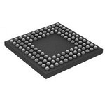
ICGOO电子元器件商城为您提供AD5379ABCZ由Analog设计生产,在icgoo商城现货销售,并且可以通过原厂、代理商等渠道进行代购。 AD5379ABCZ价格参考¥774.69-¥774.69。AnalogAD5379ABCZ封装/规格:数据采集 - 数模转换器, 14 位 数模转换器 40 108-CSPBGA(13x13)。您可以下载AD5379ABCZ参考资料、Datasheet数据手册功能说明书,资料中有AD5379ABCZ 详细功能的应用电路图电压和使用方法及教程。
| 参数 | 数值 |
| 产品目录 | 集成电路 (IC)半导体 |
| 描述 | IC DAC 14BIT 40CHAN 108CSPBGA数模转换器- DAC IC 40-CH14-Bit |
| DevelopmentKit | EVAL-AD5379EBZ |
| 产品分类 | |
| 品牌 | Analog Devices |
| 产品手册 | |
| 产品图片 |
|
| rohs | 符合RoHS无铅 / 符合限制有害物质指令(RoHS)规范要求 |
| 产品系列 | 数据转换器IC,数模转换器- DAC,Analog Devices AD5379ABCZ- |
| 数据手册 | |
| 产品型号 | AD5379ABCZ |
| 产品培训模块 | http://www.digikey.cn/PTM/IndividualPTM.page?site=cn&lang=zhs&ptm=19145http://www.digikey.cn/PTM/IndividualPTM.page?site=cn&lang=zhs&ptm=18614http://www.digikey.cn/PTM/IndividualPTM.page?site=cn&lang=zhs&ptm=26125http://www.digikey.cn/PTM/IndividualPTM.page?site=cn&lang=zhs&ptm=26140http://www.digikey.cn/PTM/IndividualPTM.page?site=cn&lang=zhs&ptm=26150http://www.digikey.cn/PTM/IndividualPTM.page?site=cn&lang=zhs&ptm=26147 |
| 产品种类 | 数模转换器- DAC |
| 位数 | 14 |
| 供应商器件封装 | 108-CSPBGA(13x13) |
| 分辨率 | 14 bit |
| 包装 | 托盘 |
| 商标 | Analog Devices |
| 安装类型 | 表面贴装 |
| 安装风格 | SMD/SMT |
| 封装 | Tray |
| 封装/外壳 | 108-BGA,CSPBGA |
| 封装/箱体 | BGA-108 |
| 工作温度 | -40°C ~ 85°C |
| 工厂包装数量 | 160 |
| 建立时间 | 20µs |
| 接口类型 | Parallel or Serial (3-Wire, Microwire, QSPI, SPI) |
| 数据接口 | 串行,并联 |
| 最大功率耗散 | 2 W |
| 最大工作温度 | + 85 C |
| 最小工作温度 | - 40 C |
| 标准包装 | 1 |
| 电压参考 | External |
| 电压源 | 模拟和数字,双 ± |
| 电源电压-最大 | +/- 16.5 V |
| 电源电压-最小 | +/- 11.4 V |
| 积分非线性 | +/- 3 LSB |
| 稳定时间 | 30 us |
| 系列 | AD5379 |
| 结构 | Resistor-String |
| 转换器数 | 40 |
| 转换器数量 | 40 |
| 输出数和类型 | 40 电压,双极 |
| 输出类型 | Voltage Buffered |
| 配用 | /product-detail/zh/EVAL-AD5379EBZ/EVAL-AD5379EBZ-ND/1649691 |
| 采样比 | 50 kSPs |
| 采样率(每秒) | 50k |


- 商务部:美国ITC正式对集成电路等产品启动337调查
- 曝三星4nm工艺存在良率问题 高通将骁龙8 Gen1或转产台积电
- 太阳诱电将投资9.5亿元在常州建新厂生产MLCC 预计2023年完工
- 英特尔发布欧洲新工厂建设计划 深化IDM 2.0 战略
- 台积电先进制程称霸业界 有大客户加持明年业绩稳了
- 达到5530亿美元!SIA预计今年全球半导体销售额将创下新高
- 英特尔拟将自动驾驶子公司Mobileye上市 估值或超500亿美元
- 三星加码芯片和SET,合并消费电子和移动部门,撤换高东真等 CEO
- 三星电子宣布重大人事变动 还合并消费电子和移动部门
- 海关总署:前11个月进口集成电路产品价值2.52万亿元 增长14.8%


PDF Datasheet 数据手册内容提取
40-Channel, 14-Bit, Parallel and Serial Input, Bipolar Voltage-Output DAC AD5379 FEATURES Interface options: Parallel interface 40-channel DAC in 13 mm × 13 mm 108-lead CSPBGA DSP/microcontroller-compatible, 3-wire serial interface Guaranteed monotonic to 14 bits 2.5 V to 5.5 V JEDEC-compliant digital levels Buffered voltage outputs SDO daisy-chaining option Output voltage span of 3.5 V × V (+) REF Power-on reset Maximum output voltage span of 17.5 V System calibration function allowing user-programmable Digital reset (RESET pin and soft reset function) offset and gain Pseudo differential outputs relative to REFGND APPLICATIONS Clear function to user-defined REFGND (CLR pin) Level setting in automatic test equipment (ATE) Simultaneous update of DAC outputs (LDAC pin) Variable optical attenuators (VOA) DAC increment/decrement mode Optical switches Channel grouping and addressing features Industrial control systems FUNCTIONAL BLOCK DIAGRAM VCC VDD VSS AGND DGND LDAC VBIAS VREF1(+) VREF1(–)REFGND A1 POWER-ON AD5379 VBIAS RESET CLR RESET FIFOEN DCEN/WR INPUT DAC VOUT0 SYNC/CS 14/ REG 14/ 14/ REG 14/ DAC 0–1 0–1 0–1 VOUT1 REG0 REG1 FIFO 14/ mc RREEGG00––11 DB13 SCLK/DB12 DIN/DB11 14/ INRPEUGT14/ 14/ DRAEGC 14/ DAC 2 DB0 CE 2 2 VOUT2 A A7 NTERF E 14/ 14/ mc RREEGG22 VVOOUUTT34 I N HI VOUT5 A0 AC M INPUT DAC VOUT6 SER/PAR E 14/ REG 14/ 14/ REG 14/ DAC 7 DIN AT 7 7 VOUT7 SCLK ST m REG7 SDO 14/ c REG7 REFGND B1 VOUT8 REFGND B2 14/ INRPEUGT14/ 14/ DRAEGC 14/ DAC 8–9 REFGND C1 8–9 8–9 VOUT9 REFGND C2 m REG8–9 VOUT10 REFGND D1 14/ c REG8–9 ×4 REFGND D2 BUSY VREF2(+) VREF2(–) REFGND A2 VOUT39 03165-001 Figure 1. AD5379—Protected by U.S. Patent No. 5,969,657. Rev. B Information furnished by Analog Devices is believed to be accurate and reliable. However, no responsibility is assumed by Analog Devices for its use, nor for any infringements of patents or other One Technology Way, P.O. Box 9106, Norwood, MA 02062-9106, U.S.A. rights of third parties that may result from its use. Specifications subject to change without notice. No license is granted by implication or otherwise under any patent or patent rights of Analog Devices. Tel: 781.329.4700 www.analog.com Trademarks and registered trademarks are the property of their respective owners. Fax: 781.461.3113 ©2004–2009 Analog Devices, Inc. All rights reserved.
AD5379 TABLE OF CONTENTS Features .............................................................................................. 1 Calibration ................................................................................... 20 Applications ....................................................................................... 1 Clear Function ............................................................................ 20 General Description ......................................................................... 3 BUSY and LDAC Functions...................................................... 20 Specifications ..................................................................................... 4 FIFO vs. Non-FIFO Operation ................................................. 21 AC Characteristics ........................................................................ 5 BUSY Input Function ................................................................ 21 Timing Characteristics ..................................................................... 6 Power-On Reset Function ......................................................... 21 Serial Interface .............................................................................. 6 RESET Input Function .............................................................. 21 Parallel Interface ........................................................................... 9 Increment/Decrement Function .............................................. 21 Absolute Maximum Ratings .......................................................... 11 Interfaces.......................................................................................... 22 ESD Caution ................................................................................ 11 Parallel Interface ......................................................................... 22 Pin Configuration and Function Descriptions ........................... 12 Serial Interface ............................................................................ 22 Terminology .................................................................................... 15 Data Decoding ................................................................................ 24 Typical Performance Characteristics ........................................... 16 Address Decoding .......................................................................... 25 Functional Description .................................................................. 18 Power Supply Decoupling ............................................................. 26 DAC Architecture—General ..................................................... 18 Power-On .................................................................................... 26 Channel Groups .......................................................................... 18 Typical Application Circuit ........................................................... 27 Transfer Function ....................................................................... 18 Outline Dimensions ....................................................................... 28 VBIAS Function ............................................................................. 19 Ordering Guide .......................................................................... 28 Reference Selection .................................................................... 19 REVISION HISTORY 7/09—Rev. A t o Rev. B Changes to Table 14 ........................................................................ 24 1/05—Rev. 0 to Rev. A Changes to Table 1 ............................................................................ 3 Change to Transfer Function Equation ....................................... 18 4/04—Revision 0: Initial Version Rev. B | Page 2 of 28
AD5379 GENERAL DESCRIPTION The AD5379 contains 40 14-bit DACs in one CSPBGA package. under the control of the WR, CS, and DAC Channel Address The AD5379 provides a bipolar output range determined by the Pins A0 to A7. It also has a 3-wire serial interface that is com- voltages applied to the VREF(+) and VREF(−) inputs. The maxi- patible with SPI®, QSPI™, MICROWIRE™, and DSP® interface mum output voltage span is 17.5 V, corresponding to a bipolar standards and can handle clock speeds of up to 50 MHz. output range of −8.75 V to +8.75 V, and is achieved with reference The DAC outputs are updated upon reception of new data into voltages of V (−) = −3.5 V and V (+) = +5 V. REF REF the DAC registers. All the outputs can be simultaneously updated The AD5379 offers guaranteed operation over a wide VSS/VDD by taking the LDAC input low. Each channel has a programmable supply range from ±11.4 V to ±16.5 V. The output amplifier gain and an offset adjust register. headroom requirement is 2.5 V operating with a load current of 1.5 mA, and 2 V operating with a load current of 0.5 mA. Each DAC output is gained and buffered on-chip with respect to an external REFGND input. The DAC outputs can also be The AD5379 contains a double-buffered parallel interface in switched to REFGND via the CLR pin. which 14 data bits are loaded into one of the input registers Table 1. High Channel Count, Low Voltage, Single-Supply DACs Model Resolution AV Range Output Channels Linearity Error (LSB) Package Description Package Option DD AD5380BST-5 14 bits 4.5 V to 5.5 V 40 ±4 100-Lead LQFP ST-100 AD5380BST-3 14 bits 2.7 V to 3.6 V 40 ±4 100-Lead LQFP ST-100 AD5381BST-5 12 bits 4.5 V to 5.5 V 40 ±1 100-Lead LQFP ST-100 AD5381BST-3 12 bits 2.7 V to 3.6 V 40 ±1 100-Lead LQFP ST-100 AD5384BBC-5 14 bits 4.5 V to 5.5 V 40 ±4 100-Lead CSPBGA BC-100 AD5384BBC-3 14 bits 2.7 V to 3.6 V 40 ±4 100-Lead CSPBGA BC-100 AD5382BST-5 14 bits 4.5 V to 5.5 V 32 ±4 100-Lead LQFP ST-100 AD5382BST-3 14 bits 2.7 V to 3.6 V 32 ±4 100-Lead LQFP ST-100 AD5383BST-5 12 bits 4.5 V to 5.5 V 32 ±1 100-Lead LQFP ST-100 AD5383BST-3 12 bits 2.7 V to 3.6 V 32 ±1 100-Lead LQFP ST-100 AD5390BST-5 14 bits 4.5 V to 5.5 V 16 ±3 52-Lead LQFP ST-52 AD5390BCP-5 14 bits 4.5 V to 5.5 V 16 ±3 64-Lead LFCSP CP-64 AD5390BST-3 14 bits 2.7 V to 3.6 V 16 ±4 52-Lead LQFP ST-52 AD5390BCP-3 14 bits 2.7 V to 3.6 V 16 ±4 64-Lead LFCSP CP-64 AD5391BST-5 12 bits 4.5 V to 5.5 V 16 ±1 52-Lead LQFP ST-52 AD5391BCP-5 12 bits 4.5 V to 5.5 V 16 ±1 64-Lead LFCSP CP-64 AD5391BST-3 12 bits 2.7 V to 3.6 V 16 ±1 52-Lead LQFP ST-52 AD5391BCP-3 12 bits 2.7 V to 3.6 V 16 ±1 64-Lead LFCSP CP-64 AD5392BST-5 14 bits 4.5 V to 5.5 V 8 ±3 52-Lead LQFP ST-52 AD5392BCP-5 14 bits 4.5 V to 5.5 V 8 ±3 64-Lead LFCSP CP-64 AD5392BST-3 14 bits 2.7 V to 3.6 V 8 ±4 52-Lead LQFP ST-52 AD5392BCP-3 14 bits 2.7 V to 3.6 V 8 ±4 64-Lead LFCSP CP-64 Rev. B | Page 3 of 28
AD5379 SPECIFICATIONS V = 2.7 V to 5.5 V; V = 11.4 V to 16.5 V; V = −11.4 V to −16.5 V; V (+) = 5 V; V (−) = −3.5 V; AGND = DGND = REFGND = 0 V; CC DD SS REF REF V = 5 V; C = 200 pF to GND; R = 11 kΩ to 3 V; gain = 1; offset = 0 V; all specifications T to T , unless otherwise noted. BIAS L L MIN MAX Table 2. Parameter A Version1 Unit Test Conditions/Comments2 ACCURACY Resolution 14 Bits Relative Accuracy ±3 LSB max −40°C to +85°C ±2.5 LSB max 0°C to 70°C Differential Nonlinearity −1/+1.5 LSB max Guaranteed monotonic by design over temperature Zero-Scale Error ±12 mV max −40°C to +85°C ±5 mV max 0°C to 70°C Full-Scale Error ±12 mV max −40°C to +85°C ±8 mV max 0°C to 70°C Gain Error ±8 mV max −40°C to +85°C ±1/±5 mV typ/max 0°C to 70°C VOUT Temperature Coefficient 5 ppm FSR/°C typ Includes linearity, offset, and gain drift (see Figure 11) DC Crosstalk2 0.5 mV max Typically 100 μV REFERENCE INPUTS2 V (+) DC Input Impedance 1 MΩ min Typically 100 MΩ REF V (−) DC Input Impedance 8 kΩ min Typically 12 kΩ REF V (+) Input Current ±10 μA max Per input (typically ±30 nA) REF V (+) Range 1.5/5 V min/max ±2% for specified operation REF V (−) Range −3.5/0 V min/max ±2% for specified operation REF REFGND INPUTS2 DC Input Impedance 80 kΩ min Typically 120 kΩ Input Range ±0.5 V min/max OUTPUT CHARACTERISTICS2 Output Voltage Range V + 2/V + 2.5 V min I = ±0.5 mA/±1.5 mA SS SS LOAD V − 2/V − 2.5 V max I = ±0.5 mA/±1.5 mA DD DD LOAD Short-Circuit Current 15 mA max Load Current ±1.5 mA max Capacitive Load 2200 pF max DC Output Impedance 1 Ω max DIGITAL INPUTS JEDEC compliant Input High Voltage 1.7 V min V = 2.7 V to 3.6 V CC 2.0 V min V = 3.6 V to 5.5 V CC Input Low Voltage 0.8 V max V = 2.7 V to 5.5 V CC Input Current (with pull-up/pull-down) ±8 μA max SER/PAR, FIFOEN, and RESET pins only Input Current (no pull-up/pull-down) ±1 μA max All other digital input pins Input Capacitance2 10 pF max DIGITAL OUTPUTS (BUSY, SDO) Output Low Voltage 0.5 V max Sinking 200 μA Output High Voltage (SDO) V − 0.5 V min Sourcing 200 μA CC High Impedance Leakage Current −70 μA max SDO only High Impedance Output Capacitance2 10 pF typ POWER REQUIREMENTS V 2.7/5.5 V min/max CC V 8.5/16.5 V min/max DD V −3/−16.5 V min/max SS Rev. B | Page 4 of 28
AD5379 Parameter A Version1 Unit Test Conditions/Comments2 Power Supply Sensitivity2 ∆ Full Scale/∆ V −75 dB typ DD ∆ Full Scale/∆ V −75 dB typ SS ∆ Full Scale/∆ V −90 dB typ CC I 5 mA max V = 5.5 V, V = V , V = GND CC CC IH CC IL I 28 mA max Outputs unloaded (typically 20 mA) DD I 23 mA max Outputs unloaded (typically 15 mA) SS Power Dissipation Power Dissipation Unloaded (P) 850 mW max V = 16.5 V, V = −16.5 V DD SS Power Dissipation Loaded (P ) 2000 mW max P = P + Σ(V − V ) × I + Σ(V − V ) × I TOTAL TOTAL DD O SOURCE O SS SINK Junction Temperature 130 °C max T = T + P × θ3 J A TOTAL J 1 Temperature range for A Version: −40°C to +85°C. Typical specifications are at 25°C. 2 Guaranteed by design and characterization, not production tested. 3 Where θJ represents the package thermal impedance. AC CHARACTERISTICS V = 2.7 V to 5.5 V; V = 11.4 V to 16.5 V; V = −11.4 V to −16.5 V; V (+) = 5 V; V (−) = −3.5 V; AGND = DGND = REFGND = 0 V; CC DD SS REF REF V = 5 V; C = 220 pF; R = 11 kΩ to 3 V; gain = 1; offset = 0 V. BIAS L L Table 3. Parameter A Version1 Unit Test Conditions/Comments DYNAMIC PERFORMANCE Output Voltage Settling Time 20 μs typ Full-scale change to ±1/2 LSB 30 μs max DAC latch contents alternately loaded with all 0s and all 1s Slew Rate 1 V/μs typ Digital-to-Analog Glitch Energy 20 nV-s typ Glitch Impulse Peak Amplitude 15 mV max Channel-to-Channel Isolation 100 dB typ V (+) = 2 V p-p, (1 V ) 1 kHz, V (−) = −1 V REF BIAS REF DAC-to-DAC Crosstalk 40 nV-s typ Between DACs inside a group (see the Terminology section) 10 nV-s typ Between DACs from different groups Digital Crosstalk 0.1 nV-s typ Digital Feedthrough 1 nV-s typ Effect of input bus activity on DAC output under test Output Noise Spectral Density @ 1 kHz 350 nV/(Hz)1/2 typ V (+) = V (−) = 0 V REF REF 1 Guaranteed by design and characterization, not production tested. Rev. B | Page 5 of 28
AD5379 TIMING CHARACTERISTICS SERIAL INTERFACE V = 2.7 V to 5.5 V; V = 11.4 V to 16.5 V; V = −11.4 V to −16.5 V; V (+) = 5 V; V (−) = −3.5 V; AGND = DGND = REFGND = 0 V; CC DD SS REF REF V = 5 V, FIFOEN = 0 V; all specifications T to T , unless otherwise noted. BIAS MIN MAX Table 4. Parameter1, 2, 3 Limit at T , T Unit Description MIN MAX t 20 ns min SCLK cycle time. 1 t 8 ns min SCLK high time. 2 t 8 ns min SCLK low time. 3 t4 10 ns min SYNC falling edge to SCLK falling edge setup time. t54 15 ns min 24th SCLK falling edge to SYNC falling edge. t64 25 ns min Minimum SYNC low time. t7 10 ns min Minimum SYNC high time. t 5 ns min Data setup time. 8 t 4.5 ns min Data hold time. 9 t104, 5 30 ns max 24th SCLK falling edge to BUSY falling edge. t11 330 ns max BUSY pulse width low (single-channel update). See Table 10. t124 20 ns min 24th SCLK falling edge to LDAC falling edge. t13 20 ns min LDAC pulse width low. t14 150 ns typ BUSY rising edge to DAC output response time. t15 0 ns min BUSY rising edge to LDAC falling edge. t16 100 ns min LDAC falling edge to DAC output response time. t 20/30 μs typ/max DAC output settling time. 17 t18 10 ns min CLR pulse width low. t19 350 ns max CLR/RESET pulse activation time. t 6, 7 25 ns max SCLK rising edge to sdo valid. 20 t217 5 ns min SCLK falling edge to SYNC rising edge. t227 5 ns min SYNC rising edge to SCLK rising edge. t237 20 ns min SYNC rising edge to LDAC falling edge. t245 30 ns min SYNC rising edge to BUSY falling edge. t25 10 ns min RESET pulse width low. t26 120 μs max RESET time indicated by BUSY low. 1 Guaranteed by design and characterization, not production tested. 2 All input signals are specified with tr = tf = 2 ns (10% to 90% of VCC), and timed from a voltage level of 1.2 V. 3 See Figure 4 and Figure 5. 4 Standalone mode only. 5 This is measured with the load circuit shown in Figure 2. 6 This is measured with the load circuit shown in Figure 3. 7 Daisy-chain mode only. VCC 200μA IOL RL 2.2kΩ TO VOH(min) + VOL(max) OUTPUT PIN CL 50pF 2 TO OUTPPUINT CL 50pF VOL 03165-002 200μA IOH 03165-003 Figure 3. Load Circuit for SDO Timing Diagram Figure 2. Load Circuit for BUSY Timing Diagram (Serial Interface, Daisy-Chain Mode) Rev. B | Page 6 of 28
AD5379 t 1 SCLK 1 2 24 24 t t 3 2 t4 t5 t7 t6 SYNC t t 8 9 DIN DB23 DB0 t 10 t 11 BUSY t t 12 13 t LDAC1 17 t 14 VOUT t 15 t 13 LDAC2 t t 17 VOUT 16 t 18 CLR t 19 VOUT 1LDAC ACTIVE DURING BUSY 2LDAC ACTIVE AFTER BUSY t 25 RESET VOUT t19 BUSY t26 03165-004 Figure 4. Serial Interface Timing Diagram (Standalone Mode) Rev. B | Page 7 of 28
AD5379 t 1 SCLK 24 48 t t3 t2 t22 7 t 21 t 4 SYNC t t 8 9 DIN D23 D0 D23' D0' INPUT WORD FOR DAC N INPUT WORD FOR DAC N+1 t 20 SDO D23 D0 UNDEFINED INPUT WORD FOR DAC N t t 23 13 LDAC t 24 BUSY t11 03165-005 Figure 5. Serial Interface Timing Diagram (Daisy-Chain Mode) Rev. B | Page 8 of 28
AD5379 PARALLEL INTERFACE V = 2.7 V to 5.5 V; V = 11.4 V to 16.5 V; V = −11.4 V to −16.5 V; AGND = DGND = DUTGND = 0 V; V (+) = 5 V; CC DD SS REF V (−) = −3.5 V, FIFOEN = 0 V; all specifications T to T , unless otherwise noted. REF MIN MAX Table 5. Parameter1, 2, 3 Limit at T to T Unit Description MIN MAX t0 4.5 ns min REG0, REG1, address to WR rising edge setup time. t1 4.5 ns min REG0, REG1, address to WR rising edge hold time. t2 10 ns min CS pulse width low. t3 10 ns min WR pulse width low. t4 0 ns min CS to WR falling edge setup time. t5 0 ns min WR to CS rising edge hold time. t6 4.5 ns min Data to WR rising edge setup time. t7 4.5 ns min Data to WR rising edge hold time. t8 20 ns min WR pulse width high. t9 240 ns min Minimum WR cycle time (single-channel write). t104 0/30 ns min/max WR rising edge to BUSY falling edge. t114 330 ns max BUSY pulse width low (single-channel update). See Table 10. t12 0 ns min BUSY rising edge to WR rising edge. t13 30 ns min WR rising edge to LDAC falling edge. t14 20 ns min LDAC pulse width low. t154 150 ns typ BUSY rising edge to DAC output response time. t16 20 ns min LDAC rising edge to WR rising edge. t17 0 ns min BUSY rising edge to LDAC falling edge. t18 100 ns typ LDAC falling edge to DAC output response time. t 20/30 μs typ/ max DAC output settling time. 19 t20 10 ns min CLR pulse width low. t21 350 ns max CLR/RESET pulse activation time. t22 10 ns min RESET pulse width low. t23 120 μs max RESET time indicated by BUSY low. 1 Guaranteed by design and characterization, not production tested. 2 All input signals are specified with tr = tf = 2 ns (10% to 90% of VCC), and timed from a voltage level of 1.2 V. 3 See Figure 6. 4 Measured with load circuit shown in Figure 2. Rev. B | Page 9 of 28
AD5379 t t 0 1 REG0, REG1, A7–A02 t t 4 5 t 2 CS t 9 t 3 WR t 8 t6 t7 t16 DB12–DB0 t 12 t 10 t 11 BUSY t t 13 14 t LDAC1 19 t 15 VOUT t17 t14 LDAC2 t t 19 VOUT 18 t 20 CLR t 21 VOUT 1LDAC ACTIVE DURING BUSY 2LDAC ACTIVE AFTER BUSY t 22 RESET VOUT t21 BUSY t23 03165-006 Figure 6. Parallel Interface Timing Diagram Rev. B | Page 10 of 28
AD5379 ABSOLUTE MAXIMUM RATINGS T = 25°C, unless otherwise noted. Stresses above those listed under Absolute Maximum Ratings A Transient currents of up to 100 mA do not cause SCR latch-up. may cause permanent damage to the device. This is a stress rating only, and functional operation of the device at these or Table 6. any other conditions above those listed in the operational Parameter Rating sections of this specification is not implied. Exposure to V to AGND −0.3 V to +17 V absolute maximum rating conditions for extended periods may DD V to AGND −17 V to +0.3 V affect device reliability. SS V to DGND −0.3 V to +7 V CC Digital Inputs to DGND −0.3 V to V + 0.3 V CC Digital Outputs to DGND −0.3 V to V + 0.3 V CC V 1(+), V 2(+) to AGND −0.3 V to +7 V REF REF V 1(−), V 2(−) to AGND V − 0.3 V to V + 0.3 V REF REF SS DD V to AGND −0.3 V to +7 V BIAS VOUT0–VOUT39 to AGND V − 0.3 V to V + 0.3 V SS DD REFGND to AGND V − 0.3 V to V + 0.3 V SS DD AGND to DGND −0.3 V to +0.3 V Operating Temperature Range (T ) A Industrial (A Version) −40°C to +85°C Storage Temperature Range −65°C to +150°C Junction Temperature (T max) 150°C J 108-Lead CSPBGA Package θ Thermal Impedance 37.5°C/W JA θ Thermal Impedance 8.5°C/W JC Reflow Soldering Peak Temperature 230°C Time at Peak Temperature 10 sec to 40 sec ESD CAUTION ESD (electrostatic discharge) sensitive device. Electrostatic charges as high as 4000 V readily accumulate on the human body and test equipment and can discharge without detection. Although this product features proprietary ESD protection circuitry, permanent damage may occur on devices subjected to high energy electrostatic discharges. Therefore, proper ESD precautions are recommended to avoid performance degradation or loss of functionality. Rev. B | Page 11 of 28
AD5379 PIN CONFIGURATION AND FUNCTION DESCRIPTIONS 1 2 3 4 5 6 7 8 9 10 11 12 A A B B C C D D E E F AD5379 F G TOP VIEW G H H J J K K L L M M 1 2 3 4 5 6 7 8 9 10 11 12 03165-007 Figure 7. Pin Configuration Table 7. 108-Lead CSPBGA Ball Configuration CSPBGA CSPBGA CSPBGA CSPBGA Number Ball Name Number Ball Name Number Ball Name Number Ball Name A1 REG0 C5 LDAC G3 BUSY K12 VOUT23 A2 VCC3 C6 VOUT8 G10 VSS3 L1 A7 A3 DB10 C7 VOUT3 G11 VOUT29 L2 A6 A4 AGND4 C8 VOUT4 G12 REFGNDC2 L3 N/C3 A5 VBIAS C9 VOUT9 H1 WR/DCEN L4 RESET2 A6 VOUT5 C10 VOUT34 H2 SDO2 L5 VOUT17 A7 AGND3 C11 VOUT32 H3 CS/SYNC L6 AGND2 A8 REFGNDA1 C12 VOUT33 H10 VOUT28 L7 VOUT14 A9 VDD5 D1 DB7 H11 VOUT26 L8 VOUT10 A10 VSS5 D2 DB8 H12 VOUT27 L9 VDD1 A11 VSS4 D3 DGND1 J1 A0 L10 VREF2(+) A12 VDD4 D10 VREF1(−) J2 A1 L11 VOUT20 B1 REG1 D11 VOUT35 J3 A2 L12 VOUT21 B2 DGND4 D12 VOUT36 J10 VOUT19 M1 DGND3 B3 DB9 E1 DB5 J11 VOUT24 M2 VCC2 B4 CLR E2 DB6 J12 VOUT25 M3 FIFOEN1 B5 VOUT7 E3 VCC1 K1 A4 M4 AGND1 B6 VOUT6 E10 REFGNDB2 K2 A5 M5 VOUT15 B7 VOUT0 E11 VOUT37 K3 A3 M6 VOUT11 B8 VOUT1 E12 VOUT38 K4 DGND2 M7 REFGNDB1 B9 VOUT2 F1 DB4 K5 REFGNDA2 M8 VREF1(+) B10 VOUT31 F2 DB3 K6 VREF2(−) M9 VSS1 B11 REFGNDD1 F3 DB2 K7 VOUT12 M10 VSS2 B12 VOUT30 F10 VDD3 K8 VOUT13 M11 VDD2 C1 DB13 F11 REFGNDD2 K9 VOUT16 M12 REFGNDC1 C2 DB12/SCLK F12 VOUT39 K10 VOUT18 C3 DB11/DIN G1 DB1 K11 VOUT22 C4 SER/PAR1 G2 DB0 1 An internal 1 MΩ pull-down device is located on this logic input; therefore, it can be left floating and defaults to a logic low condition. 2 An internal 1 MΩ pull-up device is located on this logic input; therefore, it can be left floating and defaults to a logic high condition. 3 N/C—Do not connect to this pin. Internal active pull-up device on these logic inputs. They default to a logic high condition. Rev. B | Page 12 of 28
AD5379 Table 8. Pin Function Descriptions Pin Function V (1–3) Logic Power Supply; 2.7 V to 5.5 V. These pins should be decoupled with 0.1 μF ceramic capacitors and 10 μF CC capacitors. V (1–5) Negative Analog Power Supply; −11.4 V to −16.5 V for Specified Performance. These pins should be decoupled with SS 0.1 μF ceramic capacitors and 10 μF capacitors. V (1–5) Positive Analog Power Supply; +11.4 V to +16.5 V for Specified Performance. These pins should be decoupled with DD 0.1 μF ceramic capacitors and 10 μF capacitors. AGND(1–4) Ground for All Analog Circuitry. All AGND pins should be connected to the AGND plane. DGND(1–4) Ground for All Digital Circuitry. All DGND pins should be connected to the DGND plane. V 1(+), V 1(−) Reference Inputs for DACs 0 to 7, 10 to 17, 20 to 27, and 30 to 37. These voltages are referred to AGND. REF REF V 2(+), V 2(−) Reference Inputs for DACs 8, 9, 18, 19, 28, 29, 38, and 39. These reference voltages are referred to AGND. REF REF V DAC Bias Voltage Input/Output. This pin provides an access to the on-chip voltage generator voltage and is provided BIAS for bypassing and overdriving purposes only. If V (+) > 4.25 V, V must be pulled high externally to an equal or REF BIAS higher potential (for example, 5 V). If V (+) < 4.25 V, the on-chip bias generator can be used. In this case, the V pin REF BIAS should be decoupled with a 10 nF capacitor to AGND. VOUT0 to VOUT39 DAC Outputs. Buffered analog outputs for each of the 40 DAC channels. Each analog output is capable of driving an output load of 5 kΩ to ground. Typical output impedance of these amplifiers is 1 Ω. SER/PAR Interface Select Input. This pin allows the user to select whether the serial or parallel interface is used. This pin has an internal 1 MΩ pull-down resistor, meaning that the default state at power-on is parallel mode. If this pin is tied high, the serial interface is used. SYNC1 Active Low Input. This is the frame synchronization signal for the serial interface. SCLK1 Serial Clock Input. Data is clocked into the shift register on the falling edge of SCLK. This pin operates at clock speeds up to 50 MHz. DIN1 Serial Data Input. Data must be valid on the falling edge of SCLK. SDO1 Serial Data Output. CMOS output. SDO can be used for daisy-chaining a number of devices together. Data is clocked out on SDO on the rising edge of SCLK and is valid on the falling edge of SCLK. DCEN1 Daisy-Chain Select Input (Level Sensitive, Active High). When high, this signal is used in conjunction with SER/PAR high to enable serial interface daisy-chain mode. CS Parallel Interface Chip Select Input (Level Sensitive, Active Low). If this pin is low, the device is selected. WR Parallel Interface Write Input (Edge Sensitive). The rising edge of WR is used in conjunction with CS low and the address bus inputs to write to the selected AD5379 registers. DB13 to DB0 Parallel Data Inputs. The AD5379 can accept a straight 14-bit parallel word on DB0 to DB13, where DB13 is the MSB and DB0 is the LSB. A0 to A7 Parallel Address Inputs. A7 to A4 are decoded to select one group or multiple groups of registers (input registers, gain registers (m) or offset registers (c)) for a data transfer. This pin is used in conjunction with the REG1 and REG0 pins to determine the destination register for the input data. See the Parallel Interface section for details of the address decoding. REG0 Parallel Interface Register Select Input. This pin is used together with REG1 to select data registers, gain registers, offset registers, increment/decrement mode, or the soft reset function. See Table 11. CLR Asynchronous Clear Input (Level Sensitive, Active Low). When CLR is low, the input to each of the DAC output buffer stages, VOUT0 to VOUT39, is switched to the externally set potential on the relevant REFGND pin. While CLR is low, all LDAC pulses are ignored. When CLR is taken high again, the DAC outputs remain cleared until LDAC is taken low. The contents of input registers and DAC registers 0 to 39 are not affected by taking CLR low. BUSY Digital Input/Open-Drain Output. This pin must be pulled high with a pull-up resistor for correct operation. BUSY goes low during internal calculations of x2. During this time, the user can continue writing new data to additional ×1, c, and m registers (these are stored in a FIFO), but no further updates to the DAC registers and DAC outputs can take place. If LDAC is taken low while BUSY is low, this event is stored. Because BUSY is bidirectional, it can be pulled low externally to delay LDAC action. BUSY also goes low during power-on reset or when the RESET pin is low. During a RESET operation, the parallel interface is disabled and any events on LDAC are ignored. LDAC Load DAC Logic Input (Active Low). If LDAC is taken low while BUSY is inactive (high), the contents of the input registers are transferred to the DAC registers and the DAC outputs are updated. If LDAC is taken low while BUSY is active and internal calculations are taking place, the LDAC event is stored and the DAC registers are updated when BUSY goes inactive. However, any events on LDAC during power-on reset or RESET are ignored. Rev. B | Page 13 of 28
AD5379 Pin Function FIFOEN FIFO Enable (Level Sensitive, Active High). When connected to DVDD, the internal FIFO is enabled, allowing the user to write to the device at full speed. FIFO is available in both serial and parallel mode. The FIFOEN pin has an internal 1 MΩ pull-down resistor connected to ground, meaning that the FIFO is disabled by default. RESET Asynchronous Digital Reset Input (Falling Edge Sensitive). If unused, RESET may be left unconnected; an internal pull- up resistor (1 MΩ) ensures that the RESET input is held high. The function of this pin is equivalent to that of the power- on reset generator. When this pin is taken low, the AD5379 state machine initiates a reset sequence to digitally reset x1, m, c, and x2 registers to their default power-on values. This sequence takes 100 μs (typ). Furthermore, the input to each of the DAC output buffer stages, VOUT0 to VOUT39, is switched to the externally set potential on the relevant REFGND pin. During RESET, BUSY goes low and the parallel interface is disabled. All LDAC pulses are ignored until BUSY goes high. When RESET is taken high again, the DAC ouputs remain at REFGND until LDAC is taken low. REFGNDA1 Reference Ground for DACs 0 to 7. VOUT0 to VOUT7 are referenced to this voltage. REFGNDA2 Reference Ground for DACs 8 and 9. VOUT8 and VOUT9 are referenced to this voltage. REFGNDB1 Reference Ground for DACs 10 to 17. VOUT10 to VOUT17 are referenced to this voltage. REFGNDB2 Reference Ground for DACs 18 and 19. VOUT18 and VOUT19 are referenced to this voltage. REFGNDC1 Reference Ground for DACs 20 to 27. VOUT20 to VOUT27 are referenced to this voltage. REFGNDC2 Reference Ground for DACs 28 and 29. VOUT28 and VOUT29 are referenced to this voltage. REFGNDD1 Reference Ground for DACs 30 to 37. VOUT30 to VOUT37 are referenced to this voltage. REFGNDD2 Reference Ground for DACs 38 and 39. VOUT38 and VOUT39 are referenced to this voltage. 1 These serial interface signals do not require separate pins, but share parallel interface pins. Rev. B | Page 14 of 28
AD5379 TERMINOLOGY Relative Accuracy DC Crosstalk Relative accuracy, or endpoint linearity, is a measure of the The 40 DAC outputs are buffered by op amps that share maximum deviation from a straight line passing through the common V and V power supplies. If the dc load current DD SS endpoints of the DAC transfer function. It is measured after changes in one channel (due to an update), this can result in a adjusting for zero-scale error and full-scale error and is further dc change in one or more channel outputs. This effect is expressed in least significant bits (LSB). more significant at high load currents and reduces as the load currents are reduced. With high impedance loads, the effect is Differential Nonlinearity virtually unmeasurable. Multiple V and V terminals are DD SS Differential nonlinearity is the difference between the measured provided to minimize dc crosstalk. change and the ideal 1 LSB change between any two adjacent codes. A specified differential nonlinearity of 1 LSB maximum Output Voltage Settling Time ensures monotonicity. The amount of time it takes for the output of a DAC to settle to a specified level for a full-scale input change. Zero-Scale Error Zero-scale error is the error in the DAC output voltage when all Digital-to-Analog Glitch Energy 0s are loaded into the DAC register. The amount of energy injected into the analog output at the major code transition. It is specified as the area of the glitch in Ideally, with all 0s loaded to the DAC and m is all 1s, nV-s. It is measured by toggling the DAC register data between c is 10 0000 0000 0000: 0x1FFF and 0x2000. VOUT = 2.5 × (VREF(−) − AGND) + REFGND (zero scale) Channel-to-Channel Isolation Channel-to-channel isolation refers to the proportion of input Zero-scale error is a measure of the difference between VOUT signal from one DAC’s reference input that appears at the (actual) and VOUT (ideal) expressed in mV. Zero-scale error is output of another DAC operating from another reference. It is mainly due to offsets in the output amplifier. expressed in dB and measured at midscale. Full-Scale Error DAC-to-DAC Crosstalk Full-scale error is the error in DAC output voltage when all 1s DAC-to-DAC crosstalk is the glitch impulse that appears at the are loaded into the DAC register. output of one converter due to both the digital change and Ideally, with all 1s loaded to the DAC and m is all 1s, subsequent analog output change at another converter. It is c is 10 0000 0000 0000: specified in nV-s. VOUT = 3.5 × (VREF(+) − AGND) + 2.5 × Digital Crosstalk (full scale) (VREF(−)− AGND) + REFGND The glitch impulse transferred to the output of one converter due to a change in the DAC register code of another converter is Full-scale error is a measure of the difference between VOUT defined as the digital crosstalk and is specified in nV-s. (actual) and VOUT (ideal) expressed in mV. It does not include zero-scale error. Digital Feedthrough When the device is not selected, high frequency logic activity Gain Error on the device’s digital inputs can be capacitively coupled both Gain error is the difference between full-scale error and zero- across and through the device to show up as noise on the scale error. It is expressed in mV. VOUT pins. It can also be coupled along the supply and ground lines. This noise is digital feedthrough. Gain Error = Full-Scale Error − Zero-Scale Error Output Noise Spectral Density VOUT Temperature Coefficient Output noise spectral density is a measure of internally This includes output error contributions from linearity, offset, generated random noise. Random noise is characterized as a and gain drift. spectral density (voltage per √Hz). It is measured by loading all DC Output Impedance DACs to midscale and measuring noise at the output. It is DC output impedance is the effective output source resistance. measured in nV/(Hz)1/2. It is dominated by package lead resistance. Rev. B | Page 15 of 28
AD5379 TYPICAL PERFORMANCE CHARACTERISTICS 1.5 3 VDD = +12V VSS =–12V 1.0 2 VREF(+) = +5V VREF(–) =–3.5V TMAX = +85C 1 0.5 FS B) mV) 0 LS 0 R ( INL ( ERRO –1 –0.5 ZC –2 VDD = +12V –1.0 VVSRSE F=(+–)1 =2 V+5V –3 VREF(–) =–3.5V TA = 25C –1.5 –4 0 2 4 AD65379 C8ODE (11003) 12 14 16 03165-008 –40 –20 0TEMPER2A0TURE (4C0) 60 80 03165-011 Figure 8. Typical INL Plot Figure 11. Typical Full-Scale and Zero-Scale Errors vs. Temperature 1400 19.0 VDD = +12V VDD = +12V VREF(+) = +5V VSS =–12V 18.9 VSS =–12V VREF(–) =–3.5V 1200 VREF(+) = +5V VREF(–) =–3.5V 18.8 1000 +85C 18.7 Y NC 800 A) 18.6 E m EQU 600 (DD 18.5 +25C R I F 18.4 400 –40C 18.3 200 18.2 0 18.1 –3 –2 –1INL ERR0OR (LSB)1 2 3 03165-009 10.0 10.5 11.0 11.5 12.0VD1D2 .(5V)13.0 13.5 14.0 14.5 15.0 03165-012 Figure 9. INL Error Distribution Figure 12. IDD vs. VDD over Temperature (−40°C, +25°C, +85°C Superimposed) 3 –14.6 VVDSSD == –+1122VV VVDSSD == –+1122VV VVRREEFF((–+)) == –+35.V5V 2 VREF(+) = +5V –14.8 –40C VREF(–) =–3.5V TMAX = +85C B) 1 –15.0 S L ERROR ( 0 I (mA)SS –15.2 +25C L IN –1 –15.4 –2 –15.6 +85C –3 –15.8 –40 –20 0TEMPER20ATURE (4C0) 60 80 03165-010 10.0 10.5 11.0 11.5 12.0VD1D2 .(5V)13.0 13.5 14.0 14.5 15.0 03165-013 Figure 10. Typical INL Error vs. Temperature Figure 13.ISS vs. VDD over Temperature Rev. B | Page 16 of 28
AD5379 3.5 VDD = +12V TA = 25°C VSS =–12V VDD = +12V 3.0 VVRREEFF((+–)) == –+35.V5V VOUT VVSRSE F=(+–)1 =2 V+5V VREF(–) =–3.5V 2.5 A) 2.0 m (C IC 1.5 +85°C 1.0 0.5 –40°C +25°C 02.5 3.0 3.5FREQUE4N.0CY (MHz4).5 5.0 5.5 03165-014 10V 5mV 03165-017 Figure 14. ICC vs. Supply Figure 17. DAC-to-DAC Crosstalk –0.208 1.75 TA = 25°C TA = 25°C VDD = +12V 1.70 VDD = +12V –0.211 VVSRSE F=(+–)1=2 V+5V 1.65 VVSRSE F=(+–)1 =2 V+5V VREF(–)=–3.5V VREF(–) =–3.5V 1.60 VCC = +3.3V MPLITUDE (V)––00..221174 I (mA)CC 11..5505 A 1.45 –0.220 1.40 1.35 –0.223 1.30 0 4 8TIME (μs)12 16 20 03165-015 0 0.4 0.8 IN1.P2UT VO1.L6TAGE2 (.0V) 2.4 2.8 3.2 03165-018 Figure 15. Major Code Transition Glitch Energy Figure 18. Supply Current vs. Digital Input Voltage –0.208 TA = 25°C VSS =–12V VREF(–) =–3.5V VDD = +12V VREF(+) = +5V –0.209 V) E ( D U T LI P M A –0.210 –0.211 0 1.4 2.8TIME (μs)4.2 5.6 6.0 03165-016 Figure 16. Digital Feedthrough Rev. B | Page 17 of 28
AD5379 FUNCTIONAL DESCRIPTION DAC ARCHITECTURE—GENERAL Figure 19 shows a single DAC channel and its associated registers. The power-on values for the m and c registers are full The AD5379 contains 40 DAC channels and 40 output scale and 0x2000, respectively. The user can individually adjust amplifiers in a single package. The architecture of a single DAC the voltage range on each DAC channel by overwriting the channel consists of a 14-bit resistor-string DAC followed by an power-on values of m and c. The AD5379 has digital overflow output buffer amplifier. The resistor-string section is simply a and underflow detection circuitry to clamp the DAC output at string of resistors, each of value R, from V (+) to AGND. This REF full scale or zero scale when the values chosen for x1, m, and c type of architecture guarantees DAC monotonicity. The 14-bit result in x2 being out of range. binary digital code loaded to the DAC register determines at which node on the string the voltage is tapped off before being LDAC VREF(+) fed into the output amplifier. The output amplifier translates the DAC output of the DAC to a wider range. The DAC output is gained up by a factor of 3.5 and offset by the voltage on the V (−) pin. REF x1 INPUT See the Transfer Function section for more information. REG CHANNEL GROUPS INPUT x2 x2 DAC DAC VDAC DATA REG REG m REG The 40 DAC channels on the AD5379 are arranged into four groups (A, B, C, D) of 10 channels. In each group, eight c REG channels are connected to V 1(+) and V 1(−), and the REF REF VreRmEFa2i(n−i)n.g E tawcoh cghroaunpn ehlsa sa rtwe coo innndeivcitdeud atlo R VERFEGF2N(+D) apninds . For AGND 03165-019 example, in Group A, eight channels are connected to Figure 19. Single DAC Channel REFGNDA1, and the remaining two channels are connected to The complete transfer function for the AD5379 can be REFGNDA2. In addition to an input register (x1) and a DAC represented as register (x2), each channel has a gain register (m) and an offset register (c). See Table 17. The inclusion of these registers allows VOUT = 3.5 × ((VREF(+)− AGND) × x2/214) + the user to calibrate out errors in the complete signal chain, 2.5 × (VREF(−)− AGND) + REFGND including the DAC errors. where: Table 9 shows the reference and REFGND inputs, and the x2 is the data word loaded to the resistor string DAC. m and c registers for Group A. Groups B, C, and D are similar. V (+) is the voltage at the positive reference pin. REF V (−) is the voltage at the negative reference pin. REF Table 9. Inputs and Registers for Group A Channel Reference REFGND m, c Registers Figure 20 shows the output amplifier stage of a single channel. 0 to 7 V 1(+), V 1(−) REFGNDA1 m REG0 to REG7 VDAC is the voltage output from the resistor string DAC. The REF REF c REG0 to REG7 nominal range of VDAC is 1 LSB to full scale. 8 and 9 V 2(+), V 2(−) REFGNDA2 m REG8 and REG9 REF REF c REG8 and REG9 VDAC VOUT TRANSFER FUNCTION The digital input transfer function for each DAC can be represented as VREF(–) R R 2.5R x2 = [(m + 1)/213 × x1] + (c − 2n−1) R where: REFGND 2.5R x2 is the data-word loaded to the resistor string DAC. (Default is 10 0000 0000 0000.) x1 is the 14-bit data-word written to the DAC input register. AGND 03165-020 (Default is 10 0000 0000 0000.) Figure 20. Output Amplifier Stage m is the 13-bit gain coefficient. (Default is 1 1111 1111 1111.) c is the 14-bit offset coefficient. (Default is 10 0000 0000 0000.) n is the DAC resolution (n = 14). Rev. B | Page 18 of 28
AD5379 V FUNCTION If this offset error is too large to calibrate, then adjust the BIAS negative reference value to account for this using the following The AD5379 has an on-chip voltage generator that provides a equation: bias voltage of 4.25 V (minimum). The V pin is provided for BIAS bypassing and overdriving purposes only. It is not intended to V (−) = V (−) − V /2.625 REF NEW REF A OFFSET be used as a supply or a reference. If V (+) > 4.25 V, V must REF BIAS be pulled high externally to an equal or higher potential (such Reference Selection Example as 5 V). The external voltage source should be capable of Nominal Output Range = 10 V; (−2 V to +8 V) driving a 50 μA (typical) current sink load. Offset Error = ±100 mV; Gain Error = ±3%; REFERENCE SELECTION REFGND = AGND = 0 V; The voltages applied to V (+) and V (−) determine the REF REF output voltage range and span on VOUT0 to VOUT39. If the 1) Gain Error = ±3%; offset and gain features are not used (m and c are left at their => Maximum Positive Gain Error = +3% power-on values), the required reference levels can be => Output Range incl. Gain Error = 10 + 0.03(10) = 10.3 V calculated as follows: 2) Offset Error = ±100 mV; => Maximum Offset Error Span = 2(100) mV = 0.2 V VREF(+) = (VOUT − VOUT )/3.5 min max min => Output Range including Gain Error and VREF(−) = (AGND + VOUT )/2.5 max min Offset Error = 10.3 + 0.2 = 10.5 V If the offset and gain features of the AD5379 are used, then the 3) VREF(+) and VREF(−) Calculation: required output range is slightly different. The chosen output Actual Output Range = 10.5 V, that is, −2.25 V to +8.25 V range should take into account the offset and gain errors that (centered); need to be trimmed out. Therefore, the chosen output range => V (+) = (8.25 + 2.25)/3.5 = 3 V should be larger than the actual, required range. REF V (−) = −2.25/+2.5 = −0.9 V REF The required reference levels can be calculated as follows: If the solution yields inconvenient reference levels, the user can 1. Identify the nominal output range on VOUT. adopt one of three approaches: 2. Identify the maximum offset span and the maximum gain • Use a resistor divider to divide down a convenient, higher required on the full output signal range. reference level to the required level. 3. Calculate the new maximum output range on VOUT • Select convenient reference levels above V (+) or below REF min including the expected, maximum offset and gain errors. V (−) . Modify the gain and offset registers to digitally REF max downsize the references. In this way, the user can use 4. Choose the new required VOUT and VOUT , keeping max min almost any convenient reference level, but may reduce the new VOUT limits centered on the nominal values and performance by overcompaction of the transfer function. assuming REFGND is zero (or equal to AGND). Note that VDD and VSS must provide sufficient headroom. • Use a combination of these two approaches. 5. Calculate the values of V (+) and V (−) as follows: REF REF V (+) = (VOUT − VOUT )/3.5 REF min max min V (−) = (AGND + VOUT )/2.5 REF max min In addition, when using reference values other than those suggested (V (+) = 5 V and V (−) = −3.5 V), the expected REF REF offset error component changes to V = 0.125 × (V (−) + 0.7 × V (+) ) OFFSET REF A REF A where: V (−) is the new negative reference value. REF A V (+) is the new positive reference value. REF A Rev. B | Page 19 of 28
AD5379 Software Clear CALIBRATION Loading a clear code to the x1 registers also enables the user to The user can perform a system calibration by overwriting the set VOUT0 to VOUT39 to the REFGND level. The default clear default values in the m and c registers for any individual DAC code corresponds to m at full-scale and c at midscale (x2 = x1). channel as follows: Default Clear Code • Calculate the nominal offset and gain coefficients for the = 214 × (−Output Offset)/(Output Range) new output range (see previous example). = 214 × 2.5 × (AGND − V (−))/(3.5 × (V (+)− AGND)) REF REF • Calculate the new m and c values for each channel based The more general expression for the clear code is as follows: on the specified offset and gain errors. Clear Code = (214)/(m + 1) × (Default Clear Code − c) Calibration Example Nominal Offset Coefficient = 0 BUSY AND LDAC FUNCTIONS Nominal Gain Coefficient = The value of x2 is calculated each time the user writes new data 10/10.5 × 8191 = 0.95238 × 8191 = 7801 to the corresponding x1, c, or m registers. During the calcula- tion of x2, the BUSY output goes low. While BUSY is low, the Example 1: Channel 0, Gain Error = 3%, Offset Error = 100 mV 1) Gain Error (3%) Calibration: 7801 × 1.03 = 8035 user can continue writing new data to the x1, m, or c registers, => Load Code “1 1111 0110 0011” to m Register 0 but no DAC output updates can take place. The DAC outputs are updated by taking the LDAC input low. If LDAC goes low 2) Offset Error (100 mV) Calibration: while BUSY is active, the LDAC event is stored and the DAC LSB Size = 10.5/16384 = 641 μV; outputs update immediately after BUSY goes high. A user can Offset Coefficient for 100 mV Offset = 100/0.64 = 156 LSBs also hold the LDAC input permanently low. In this case, the => Load “10 0000 1001 1100” to c Register 0 DAC outputs update immediately after BUSY goes high. Example 2: Channel 1, Gain Error = −3%, Offset Error = −100 mV 1) Gain Error (−3%) Calibration: 7801 × 0.97 = 7567 Table 10. BUSY Pulse Width => Load Code “1 1110 1000 1111” to m Register 1 BUSY Pulse Width (ns max) 2) Offset Error (−100 mV) Calibration: FIFO FIFO Action Enabled Disabled LSB Size = 10.5/16384 = 641 μV; Loading x1, c, or m to 1 channel 530 330 Offset Coefficient for −100 mV Offset = −100/0.64 = −156 LSBs Loading x1, c, or m to 2 channels 700 500 => Load “01 1111 0110 0100” to c Register 1 Loading x1, c, or m to 3 channels 900 700 CLEAR FUNCTION Loading x1, c, or m to 4 channels 1050 850 Loading x1, c, or m to all The clear function on the AD5379 can be implemented in 40 channels 5500 5300 hardware or software. Hardware Clear The value of x2 for a single channel or group of channels is recalculated each time there is a write to any x1 register(s), Bringing the CLR pin low switches the outputs, VOUT0 to c register(s), or m register(s). During the calculation of x2, VOUT39, to the externally set potential on the REFGND pin. BUSY goes low. The duration of this BUSY pulse depends on This is achieved by switching in REFGND and reconfiguring the number of channels being updated. For example, if x1, c, or the output amplifier stages into unity gain buffer mode, thus m data is written to one DAC channel, BUSY goes low for ensuring VOUT = REFGND. The contents of the input registers 550 ns (maximum). However, if data is written to two DAC and DAC registers are not affected by taking CLR low. When channels, BUSY goes low for 700 ns (maximum). As shown in CLR is brought high, the DAC outputs remain cleared until Table 10, there are approximately 200 ns of overhead due to LDAC is taken low. While CLR is low, the value of LDAC is FIFO access. ignored. The AD5379 contains an extra feature whereby a DAC register is not updated unless its x2 register has been written to since the last time LDAC was brought low. Normally, when LDAC is brought low, the DAC registers are filled with the contents of the x2 registers. However the AD5379 updates the DAC register only if the x2 data has changed, thereby removing unnecessary digital crosstalk. Rev. B | Page 20 of 28
AD5379 FIFO VS. NON-FIFO OPERATION externally set potential on the REFGND pin. During power-on, Two modes of operation are available for loading data to the the parallel interface is disabled, so it is not possible to write to AD5379 registers: operation with FIFO disabled and operation the part. Any transitions on LDAC during the power-on period with FIFO enabled. Operation with FIFO disabled is optimum are ignored in order to reject initial LDAC pin glitching. A for single writes to the device. If the system requires significant rising edge on BUSY indicates that power-on is complete and data transfers to the AD5379, however, then operation with that the parallel interface is enabled. All DACs remain in their FIFO enabled is more efficient. power-on state until LDAC is used to update the DAC outputs. When FIFO is enabled, the AD5379 uses an internal FIFO RESET INPUT FUNCTION memory to allow high speed successive writes in both serial and The AD5379 can be placed in its power-on reset state at any parallel modes. This optimizes the interface speed and efficiency, time by activating the RESET pin. The AD5379 state machine minimizes the total conversion time due to internal digital initiates a reset sequence to digitally reset the x1, m, c, and x2 efficiencies, and minimizes the overhead on the master con- registers to their default power-on values. This sequence takes troller when managing the data transfers. The BUSY signal goes 95 μs (typical), 120 μs (maximum), 70 μs (minimum). During low while instructions in the state machine are being executed. this sequence, BUSY goes low. While RESET is low, any Table 10 compares operation with FIFO enabled and FIFO transitions on LDAC are ignored. As with the CLR input, while disabled for different data transfers to the AD5379. Operation RESET is low, the DAC outputs are switched to REFGND. The with FIFO enabled is more efficient for all operations except outputs remain at REFGND until an LDAC pulse is applied. single write operations. When using the FIFO, the user can This reset function can also be implemented via the parallel continue writing new data to the AD5379 while write instruc- interface by setting the REG0 and REG1 pins low and writing tions are being executed. Up to 128 successive instructions can all 1s to DB13 to DB0 (see Table 16 for soft reset). be written to the FIFO at maximum speed. When the FIFO is full, additional writes to the AD5379 are ignored. INCREMENT/DECREMENT FUNCTION The AD5379 has a special function register that enables the user BUSY INPUT FUNCTION to increment or decrement the internal 14-bit input register If required, because the BUSY pin is bidirectional and open- data (x1) in steps of 0 to 127 LSBs. The increment/decrement drain1, a second AD5379 (or other device, such as a system function is selected by setting both REG1 and REG0 pins (or controller), can pull BUSY low to delay DAC update(s). This is a bits) low. Address Pins (or Bits) A7 to A0 are used to select a means of delaying any LDAC action. This feature allows DAC channel or group of channels. The amount by which the synchronous updates of multiple AD5379 devices in a system, at x1 register is incremented or decremented is determined by the maximum speed. As soon as the last device connected to the DB6 to DB0 bits/pins. For example, for a 1 LSB increment or BUSY pin is ready, all DACs update automatically. Tying the decrement, DB6 to DB0 = 0000001, while for a 7 LSB increment BUSY pin of multiple devices together enables synchronous or decrement, DB6 to DB0 = 0000111. DB8 determines whether updating of all DACs without extra hardware. the input register data is incremented (DB8 = 1) or decre- mented (DB8 = 0). The maximum amount by which the user is POWER-ON RESET FUNCTION allowed to increment or decrement the data is 127 LSBs, that is, The AD5379 contains a power-on reset generator and state DB6 to DB0 = 1111111. The 0 LSB step is included to facilitate machine. During power-on, CLR becomes active (internally), software loops in the user’s application. See Table 15. the power-on state machine resets all internal registers to their The AD5379 has digital overflow and underflow detection default values, and BUSY goes low. This sequence takes 8 ms circuitry to clamp at full scale or zero scale when the values (typical). The outputs, VOUT0 to VOUT39, are switched to the chosen for increment or decrement mode are out of range. 1 For correct operation, use pull-up resistor to digital supply. Rev. B | Page 21 of 28
AD5379 INTERFACES A7 to A0 Pins The AD5379 contains a serial and a parallel interface. The active interface is selected via the SER/PAR pin. Each of the 40 DAC channels can be individually addressed. In addition, several channel groupings enable the user to simulta- The AD5379 uses an internal FIFO memory to allow high neously write the same data to multiple DAC channels. Address speed successive writes in both serial and parallel modes. The Bits A7 to A4 are decoded to select one group or multiple user can continue writing new data to the AD5379 while write groups of registers. Address Bits A3 to A0 select one of ten instructions are being executed. The BUSY signal goes low while input data registers (x1), offset registers (c), or gain registers instructions in the FIFO are being executed. Up to 120 successive (m). See Table 17. instructions can be written to the FIFO at maximum speed. SERIAL INTERFACE When the FIFO is full, additional writes to the AD5379 are ignored. The SER/PAR pin must be tied high to enable the serial inter- face and disable the parallel interface. The serial interface is To minimize both the power consumption of the device and controlled by five pins, as follows. on-chip digital noise, the active interface powers up fully only when the device is being written to, that is, on the falling edge SYNC, DIN, SCLK of WR or on the falling edge of SYNC. Standard 3-wire interface pins. All digital interfaces are 2.5 V LVTTL-compatible when DCEN operating from a 2.7 V to 3.6 V V supply. CC Selects standalone mode or daisy-chain mode. PARALLEL INTERFACE SDO A pull-down on the SER/PAR pin makes the parallel interface Data out pin for daisy-chain mode. the default. If using the parallel interface, the SER/PAR pin can be left unconnected. Figure 6 shows the timing diagram for a Figure 4 and Figure 5 show the timing diagrams for a serial parallel write to the AD5379. The parallel interface is controlled write to the AD5379 in standalone and daisy-chain modes, by the following pins. respectively. CS Pin The 24-bit data word format for the serial interface is shown in Figure 21. Active low device select pin. MSB LSB WR Pin A7–A0 REG1 REG0 DB13–DB0 On the rising edge of WR, with CS low, the address values at Pin A7 to Pin A0 are latched, and data values at Pin DB13 to PRiEnG D1B, R0 EarGe0 lo Paidnesd into the selected AD5379 input registers. GSERLOEUCPT/C BHITASNNEL RBEITGSISTER SELECT REGISTER DATA BITS 03165-021 Figure 21. Serial Data Format The REG1 and REG0 pins determine the destination register of the data being written to the AD5379. See Table 11. Standalone Mode By connecting the DCEN (daisy-chain enable) pin low, Table 11. Register Selection standalone mode is enabled. The serial interface works with REG1 REG0 Register Selected both a continuous and a burst serial clock. The first falling edge 1 1 Input data register (x1) of SYNC starts the write cycle and resets a counter that counts 1 0 Offset register (c) the number of serial clocks to ensure that the correct number of 0 1 Gain register (m) bits is shifted into the serial shift register. Additional edges on 0 0 Special function register SYNC are ignored until 24 bits are shifted into the register. Once 24 bits are shifted into the serial shift register, the SCLK is ignored. In order for another serial transfer to take place, the DB13 to DB0 Pins counter must be reset by the falling edge of SYNC. The AD5379 accepts a straight, 14-bit parallel word on Pin DB0 to Pin DB13, where Pin DB13 is the MSB and Pin DB0 is the LSB. See Table 12, Table 13, Table 14, Table 15, and Table 16. Rev. B | Page 22 of 28
AD5379 Daisy-Chain Mode clock cycles must equal 24N, where N is the total number of AD5379 devices in the chain. If fewer than 24 clocks are For systems that contain several DACs, the SDO pin can be applied, the write sequence is ignored. used to daisy-chain several devices together. This daisy-chain mode can be useful in system diagnostics and in reducing the When the serial transfer to all devices has been completed, number of serial interface lines. SYNC is taken high. This latches the input data in each device in the daisy chain and prevents any additional data from being Connecting the DCEN (daisy-chain enable) pin high enables clocked into the input shift register. daisy-chain mode. The first falling edge of SYNC starts the write cycle. The SCLK is continuously applied to the input shift A continuous SCLK source can be used if SYNC is held low for register when SYNC is low. If more than 24 clock pulses are the correct number of clock cycles. Alternatively, a burst clock applied, the data ripples out of the shift register and appears on containing the exact number of clock cycles can be used and the SDO line. This data is clocked out on the rising edge of SYNC taken high after the final clock to latch the data. SCLK and is valid on the falling edge. By connecting this line to the DIN input on the next device in the chain, a multidevice When the transfer to all input registers is complete, a common interface is constructed. For each AD5379 in the system, LDAC signal updates all DAC registers, and all analog outputs 24 clock pulses are required. Therefore, the total number of are simultaneously updated. Rev. B | Page 23 of 28
AD5379 DATA DECODING The AD5379 contains a 14-bit data bus, DB13 to DB0. Depend- Table 14. Gain Data Format (REG1 = 0, REG0 = 1) ing on the values of REG1 and REG0, this data is loaded into DB13 to DB1 Gain the addressed DAC input register(s), offset (c) register(s), gain 1 1111 1111 1111 8192/8192 (m) register(s), or the special function register. 1 1111 1111 1110 8191/8192 1 0000 0000 0001 4098/8192 Table 12. DAC Data Format (REG1 = 1, REG0 = 1) 1 0000 0000 0000 4097/8192 DB13 to DB0 DAC Output 0 1111 1111 1111 4096/8192 11 1111 1111 1111 (16383/16384) VREF(+) V 0 0000 0000 0001 2/8192 11 1111 1111 1110 (16382/16384) VREF(+) V 0 0000 0000 0000 1/8192 10 0000 0000 0001 (8193/16384) V (+) V REF 10 0000 0000 0000 (8192/16384) V (+) V Table 15. Special Function Data Format (REG1 = 0, REG0 = 0) REF 01 1111 1111 1111 (8191/16384) V (+) V DB13 to DB0 Increment/Decrement Step (LSB) REF 00 0000 0000 0001 (1/16384) V (+) V 00000 10 1111111 +127 REF 00 0000 0000 0000 0 V 00000 10 0000111 +7 00000 10 0000001 +1 Table 13. Offset Data Format (REG1 = 1, REG0 = 0) 00000 X0 0000000 0 DB13 to DB0 Offset (LSB) 00000 00 0000001 −1 11 1111 1111 1111 +8191 00000 00 0000111 −7 11 1111 1111 1110 +8190 00000 00 1111111 −128 10 0000 0000 0001 +1 10 0000 0000 0000 +0 Table 16. Soft Reset (REG1 = 0, REG0 = 0) 01 1111 1111 1111 −1 DB13 to DB0 DAC Output 00 0000 0000 0001 −8191 11 1111 1111 1111 REFGND 00 0000 0000 0000 −8192 Rev. B | Page 24 of 28
AD5379 ADDRESS DECODING The AD5379 contains an 8-bit address bus, A7 to A0. This The REG1 and REG0 bits in the special function register (SFR) address bus allows each DAC input register (x1), each offset (c) (see Table 9) show the decoding for data, offset, and gain register, and each gain (m) register to be individually updated. registers. Note that when all 40 DAC channels are selected, Address Bit A3 to Address Bit A0 are ignored. Table 17. DAC Group Addressing A7 A6 A5 A4 Group A3 A2 A1 A0 Data/Offset/Gain/INC-DEC Register 0 0 0 0 All 40 DACs 0 0 0 0 Register 0 0 0 0 1 Group A 0 0 0 1 Register 1 0 0 1 0 Group B 0 0 1 0 Register 2 0 0 1 1 Groups A, B 0 0 1 1 Register 3 0 1 0 0 Group C 0 1 0 0 Register 4 0 1 0 1 Groups A, C 0 1 0 1 Register 5 0 1 1 0 Groups B, C 0 1 1 0 Register 6 0 1 1 1 Groups A, B, C 0 1 1 1 Register 7 1 0 0 0 Group D 1 0 0 0 Register 8 1 0 0 1 Groups A, D 1 0 0 1 Register 9 1 0 1 0 Groups B, D 1 0 1 1 Groups A, B, D 1 1 0 0 Groups C, D 1 1 0 1 Groups A, C, D 1 1 1 0 Groups B, C, D 1 1 1 1 Groups A, B, C, D Rev. B | Page 25 of 28
AD5379 POWER SUPPLY DECOUPLING and reduce the effects of glitches on the power supply line. Fast In any circuit where accuracy is important, careful considera- switching digital signals should be shielded with digital ground tion of the power supply and ground return layout helps to to avoid radiating noise to other parts of the board, and should ensure the rated performance. The printed circuit board on never be run near the reference inputs. It is essential to mini- which the AD5379 is mounted should be designed so that the mize noise on all V (+) and V (−) lines. The V pin should analog and digital sections are separated and confined to REF REF BIAS be decoupled with a 10 nF capacitor to AGND. certain areas of the board. If the AD5379 is in a system where multiple devices require an AGND-to-DGND connection, the Avoid crossover of digital and analog signals. Traces on connection should be made at one point only. The star ground opposite sides of the board should run at right angles to each point should be established as close as possible to the device. other. This reduces the effects of feedthrough through the For supplies with multiple pins (V , V , V ), it is recom- SS DD CC board. A microstrip technique is by far the best, but not always mended to tie these pins together and to decouple each possible with a double-sided board. In this technique, the supply once. component side of the board is dedicated to ground plane, while signal traces are placed on the solder side. The AD5379 should have ample supply decoupling of 10 μF in parallel with 0.1 μF on each supply located as close to the As is the case for all thin packages, care must be taken to avoid package as possible, ideally right up against the device. The flexing the CSPBGA package and to avoid a point load on the 10 μF capacitors are the tantalum bead type. The 0.1 μF capaci- surface of this package during the assembly process. tor should have low effective series resistance (ESR) and effective series inductance (ESI), such as the common ceramic POWER-ON types that provide a low impedance path to ground at high An on-chip power supply monitor makes the AD5379 robust to frequencies, to handle transient currents due to internal power sequencing. The supply monitor powers up the analog logic switching. section after (V − V ) is greater than 7 V (typical). The DD SS output buffers power-up in CLR mode forced to the DUTGND Digital lines running under the device should be avoided, potential, even if V remains at 0 V. After V is applied, the because these couple noise onto the device. The analog ground CC SS analog circuitry powers up, and the buffered DAC output level plane should be allowed to run under the AD5379 to avoid settles linearly within the supply range. noise coupling. The power supply lines of the AD5379 should use as large a trace as possible to provide low impedance paths Rev. B | Page 26 of 28
AD5379 TYPICAL APPLICATION CIRCUIT The high channel count of the AD5379 makes it well-suited to In addition to the DAC levels required in the ATE system as applications requiring high levels of integration such as optical shown in Figure 22, drivers, loads, comparators, and parametric and automatic test equipment (ATE) systems. Figure 22 shows measurement unit functions are also required. Analog Devices the AD5379 as it would be used in an ATE system. Shown here provides solutions for all these functions. is one pin of a typical logic tester. It is apparent that a number of discrete levels are required for the pin driver, active load circuit, parametric measurement unit, comparators, and clamps. DRIVEN SHIELD DAC CENTRAL PMU ADC GUARD AMP DAC PPMU DAC VCH ADC DAC TIMING DATA VTERM MEMORY DAC VH RELAYS 50Ω COAX DUT TIMING GENERATOR FORMATTER DE-SKEW DLL LOGIC DRIVER DAC VL VCL DAC DAC GND SENSE VTH COMPARE FORMATTER DE-SKEW MEMORY COMP VTL DAC DAC DEVICE POWER ACTIVE LOAD SUPPLY ADC IOL DAC VCOM DAC DAC IOH 03165-022 Figure 22. Typical Application Circuit for Logic Tester Rev. B | Page 27 of 28
AD5379 OUTLINE DIMENSIONS A1 CORNER INDEX AREA 13.00 BSC SQ 1211109 8 7 6 5 4 3 2 1 A BALL A1 B INDICATOR C D E 11.00 TOP VIEW BSC SQ BOTTOM F VIEW G H J K L M 1.00 BSC *1.85 DETAIL A 1.70 1.55 DETAIL A 1.05 1.00 0.90 0.75 0.70 0.65 0.12 MAX SEATING COPLANARITY *0.64 TYP PLANE BALL DIAMETER * CTOHME PELXICAENPTT WIOITNH O JFE PDAECCK SATGAEN DHAERIGDHST M AON-D19 B2A-ALALD D-1IA WMIETTHER. 012006-0 Figure 23. 108-Ball Chip Scale Package Ball Grid Array [CSP_BGA] (BC-108-2) Dimensions shown in millimeters ORDERING GUIDE Model Temperature Range Linearity Error (LSBs) Package Description Package Option AD5379ABC −40°C to +85°C ±3 108-Ball CSP_BGA BC-108-2 AD5379ABCZ1 −40°C to +85°C ±3 108-Ball CSP_BGA BC-108-2 EVAL-AD5379EBZ1 Evaluation Board and Software 1 Z = RoHS Compliant Part. ©2004–2009 Analog Devices, Inc. All rights reserved. Trademarks and registered trademarks are the property of their respective owners. D03165-0-7/09(B) Rev. B | Page 28 of 28