ICGOO在线商城 > 集成电路(IC) > 数据采集 - 数模转换器 > AD5348BCPZ
 Datasheet下载
- 型号: AD5348BCPZ
- 制造商: Analog
- 库位|库存: xxxx|xxxx
- 要求:
| 数量阶梯 | 香港交货 | 国内含税 |
| +xxxx | $xxxx | ¥xxxx |
查看当月历史价格
查看今年历史价格
AD5348BCPZ产品简介:
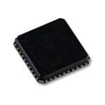
ICGOO电子元器件商城为您提供AD5348BCPZ由Analog设计生产,在icgoo商城现货销售,并且可以通过原厂、代理商等渠道进行代购。 AD5348BCPZ价格参考。AnalogAD5348BCPZ封装/规格:数据采集 - 数模转换器, 12 位 数模转换器 8 40-LFCSP-WQ(6x6)。您可以下载AD5348BCPZ参考资料、Datasheet数据手册功能说明书,资料中有AD5348BCPZ 详细功能的应用电路图电压和使用方法及教程。
AD5348BCPZ 是由 Analog Devices Inc.(现为 ADI 公司)生产的一款 8 通道、12 位电压输出数模转换器(DAC),属于数据采集系统中的核心元件之一。其应用场景广泛,主要集中在需要多通道精确控制和信号生成的领域。以下是该型号的主要应用场景:

1. 工业自动化与过程控制
   在工业控制系统中,AD5348BCPZ 可用于实现多路模拟信号的输出控制,例如调节阀门开度、电机速度或压力传感器的校准。它支持高达 8 路独立 DAC 输出,能够满足复杂工业环境下的多点控制需求。

2. 测试与测量设备
   该器件适用于各种测试仪器,如信号发生器、示波器校准设备等。通过精准的数字到模拟转换,可以生成高精度的测试信号,用于验证电子电路性能或校准其他测量设备。

3. 通信系统
   在通信领域,AD5348BCPZ 可用于生成参考电压或调整增益,以优化射频(RF)和基带信号处理模块的性能。其低功耗特性也使其适合便携式或电池供电的通信设备。

4. 医疗设备
   医疗仪器如超声设备、心电图机(ECG)和患者监护仪可能需要多通道 DAC 来生成刺激信号或校准传感器输入。AD5348BCPZ 的高分辨率和稳定性非常适合这些应用。

5. 消费类电子产品
   在音频设备中,该 DAC 可用于将数字音频信号转换为模拟信号,从而驱动扬声器或耳机。此外,在家用自动化系统中,它也可用于控制灯光亮度、温度设置等功能。

6. 汽车电子
   汽车行业中,AD5348BCPZ 可应用于车载信息娱乐系统、驾驶辅助系统(ADAS)以及发动机管理系统的信号生成与控制。

总结来说,AD5348BCPZ 凭借其多通道设计、12 位分辨率和较低的成本优势,在需要高性能、低成本解决方案的应用场景中表现出色。
| 参数 | 数值 |
| 产品目录 | 集成电路 (IC)半导体 |
| 描述 | IC DAC 12BIT OCTAL VOUT 40LFCSP数模转换器- DAC Octal 12-B Vout w/ Serial ITF IC |
| 产品分类 | |
| 品牌 | Analog Devices |
| 产品手册 | |
| 产品图片 |
|
| rohs | 符合RoHS无铅 / 符合限制有害物质指令(RoHS)规范要求 |
| 产品系列 | 数据转换器IC,数模转换器- DAC,Analog Devices AD5348BCPZ- |
| 数据手册 | |
| 产品型号 | AD5348BCPZ |
| PCN组件/产地 | |
| 产品培训模块 | http://www.digikey.cn/PTM/IndividualPTM.page?site=cn&lang=zhs&ptm=19145http://www.digikey.cn/PTM/IndividualPTM.page?site=cn&lang=zhs&ptm=18614http://www.digikey.cn/PTM/IndividualPTM.page?site=cn&lang=zhs&ptm=26125http://www.digikey.cn/PTM/IndividualPTM.page?site=cn&lang=zhs&ptm=26140http://www.digikey.cn/PTM/IndividualPTM.page?site=cn&lang=zhs&ptm=26150http://www.digikey.cn/PTM/IndividualPTM.page?site=cn&lang=zhs&ptm=26147 |
| 产品种类 | 数模转换器- DAC |
| 位数 | 12 |
| 供应商器件封装 | 40-LFCSP (6x6) |
| 分辨率 | 12 bit |
| 包装 | 托盘 |
| 商标 | Analog Devices |
| 安装类型 | 表面贴装 |
| 安装风格 | SMD/SMT |
| 封装 | Tray |
| 封装/外壳 | 40-VFQFN 裸露焊盘,CSP |
| 封装/箱体 | LFCSP-40 |
| 工作温度 | -40°C ~ 105°C |
| 工厂包装数量 | 490 |
| 建立时间 | 8µs |
| 接口类型 | Parallel |
| 数据接口 | 并联 |
| 最大功率耗散 | 8.3 mW |
| 最大工作温度 | + 105 C |
| 最小工作温度 | - 40 C |
| 标准包装 | 1 |
| 电压参考 | External |
| 电压源 | 单电源 |
| 电源电压-最大 | 5.5 V |
| 电源电压-最小 | 2.5 V |
| 积分非线性 | +/- 16 LSB |
| 稳定时间 | 8 us |
| 系列 | AD5348 |
| 结构 | Resistor String |
| 转换器数 | 8 |
| 转换器数量 | 8 |
| 输出数和类型 | 8 电压,单极8 电压,双极 |
| 输出类型 | Voltage |
| 采样比 | 125 kSPs |
| 采样率(每秒) | 125k |


- 商务部:美国ITC正式对集成电路等产品启动337调查
- 曝三星4nm工艺存在良率问题 高通将骁龙8 Gen1或转产台积电
- 太阳诱电将投资9.5亿元在常州建新厂生产MLCC 预计2023年完工
- 英特尔发布欧洲新工厂建设计划 深化IDM 2.0 战略
- 台积电先进制程称霸业界 有大客户加持明年业绩稳了
- 达到5530亿美元!SIA预计今年全球半导体销售额将创下新高
- 英特尔拟将自动驾驶子公司Mobileye上市 估值或超500亿美元
- 三星加码芯片和SET,合并消费电子和移动部门,撤换高东真等 CEO
- 三星电子宣布重大人事变动 还合并消费电子和移动部门
- 海关总署:前11个月进口集成电路产品价值2.52万亿元 增长14.8%


PDF Datasheet 数据手册内容提取
2.5 V to 5.5 V, Parallel Interface Octal Voltage Output 8-/10-/12-Bit DACs Data Sheet AD5346/AD5347/AD5348 FEATURES GENERAL DESCRIPTION AD5346: octal 8-bit DAC The AD5346/AD5347/AD53481 are octal 8-, 10-, and 12-bit AD5347: octal 10-bit DAC DACs, operating from a 2.5 V to 5.5 V supply. These devices AD5348: octal 12-bit DAC incorporate an on-chip output buffer that can drive the output Low power operation: 1.4 mA (max) at 3.6 V to both supply rails, and also allow a choice of buffered or Power-down to 120 nA at 3 V, 400 nA at 5 V unbuffered reference input. Guaranteed monotonic by design over all codes The AD5346/AD5347/AD5348 have a parallel interface. CS Rail-to-rail output range: 0 V to V or 0 V to 2 × V REF REF selects the device and data is loaded into the input registers on Power-on reset to 0 V the rising edge of WR. A readback feature allows the internal Simultaneous update of DAC outputs via LDAC pin DAC registers to be read back through the digital port. Asynchronous CLR facility Readback The GAIN pin on these devices allows the output range to be Buffered/unbuffered reference inputs set at 0 V to VREF or 0 V to 2 × VREF. 20 ns WR time Input data to the DACs is double-buffered, allowing simultane- 38-lead TSSOP/6 mm × 6 mm 40-lead LFCSP packaging ous update of multiple DACs in a system using the LDAC pin. Temperature range: –40°C to +105°C APPLICATIONS An asynchronous CLR input is also provided, which resets the contents of the input register and the DAC register to all zeros. Portable battery-powered instruments These devices also incorporate a power-on reset circuit that Digital gain and offset adjustment ensures that the DAC output powers on to 0 V and remains Programmable voltage and current sources there until valid data is written to the device. Optical networking Automatic test equipment All three parts are pin compatible, which allows users to select Mobile communications the amount of resolution appropriate for their application Programmable attenuators without redesigning their circuit board. Industrial process control FUNCTIONAL BLOCK DIAGRAM VDD AGND DGND VREFAB VREFCD AD5348 POWER-ON RESET BUF INPUT DAC STRING GAIN REGISTER REGISTER DAC A BUFFER VOUTA DB1...1 REINGPISUTTER REGDIASCTER SDTARCIN BG BUFFER VOUTB DB0 REINGPISUTTER REGDIASCTER SDTARCIN CG BUFFER VOUTC CS IFNATCEER- REINGPISUTTER REGDIASCTER SDTARCIN DG BUFFER VOUTD RD LOGIC WR REINGPISUTTER REGDIASCTER SDTARCIN EG BUFFER VOUTE A2 REINGPISUTTER REGDIASCTER SDTARCIN FG BUFFER VOUTF A1 REINGPISUTTER REGDIASCTER SDTARCIN GG BUFFER VOUTG A0 REINGPISUTTER REGDIASCTER SDTARCIN HG BUFFER VOUTH CLR LDAC POWLEORG-DICOWN 03331-0-001 VREFGH VREFEF PD Figure 1. 1 Protected by U.S. Patent No. 5,969,657. Rev. A Document Feedback Information furnished by Analog Devices is believed to be accurate and reliable. However, no responsibility is assumed by Analog Devices for its use, nor for any infringements of patents or other One Technology Way, P.O. Box 9106, Norwood, MA 02062-9106, U.S.A. rights of third parties that may result from its use. Specifications subject to change without notice. No license is granted by implication or otherwise under any patent or patent rights of Analog Devices. Tel: 781.329.4700 ©2003–2015 Analog Devices, Inc. All rights reserved. Trademarks and registered trademarks are the property of their respective owners. Technical Support www.analog.com
AD5346/AD5347/AD5348 Data Sheet TABLE OF CONTENTS Features .............................................................................................. 1 Parallel Interface ......................................................................... 17 Applications ....................................................................................... 1 Power-On Reset .......................................................................... 18 General Description ......................................................................... 1 Power-Down Mode .................................................................... 18 Functional Block Diagram .......................................................... 1 Suggested Data Bus Formats ..................................................... 19 Revision History ............................................................................... 2 Applications Information .............................................................. 20 Specifications ..................................................................................... 3 Typical Application Circuits ..................................................... 20 AC Characteristics ........................................................................ 5 Bipolar Operation Using the AD5346/AD5347/AD5348 ..... 20 Timing Characteristics ................................................................ 5 Decoding Multiple AD5346/AD5347/AD5348s .................... 21 Absolute Maximum Ratings ............................................................ 7 AD5346/AD5347/AD5348 as Digitally Programmable ESD Caution .................................................................................. 7 Window Detectors ...................................................................... 21 Pin Configurations and Function Descriptions ........................... 8 Programmable Current Source ................................................ 21 Terminology .................................................................................... 11 Coarse and Fine Adjustment Using the AD5346/AD5347/AD5348 ....................................................... 22 Typical Performance Characteristics ........................................... 13 Power Supply Bypassing and Grounding ................................ 22 Functional Description .................................................................. 17 Outline Dimensions ....................................................................... 23 Digital-to-Analog Section ......................................................... 17 Ordering Guide .......................................................................... 24 Resistor String ............................................................................. 17 DAC Reference Input ................................................................. 17 Output Amplifier ........................................................................ 17 REVISION HISTORY 6/15—Rev. 0 to Rev. A Changes to Figure 6 .......................................................................... 8 Changes to Figure 8 .......................................................................... 9 Changes to Figure 10 ...................................................................... 10 Deleted Driving V from the Reference Voltage Section and DD Figure 42; Renumbered Sequentially ........................................... 20 Deleted Table 9 and Table 10; Renumbered Sequentially ......... 23 Updated Outline Dimensions ....................................................... 23 Changes to Ordering Guide .......................................................... 24 11/03—Revision 0: Initial Version Rev. A | Page 2 of 24
Data Sheet AD5346/AD5347/AD5348 SPECIFICATIONS VDD = 2.5 V to 5.5 V; VREF = 2 V; RL = 2 kΩ to GND; CL = 200 pF to GND; all specifications TMIN to TMAX, unless otherwise noted. Table 1. B Version1 Parameter2 Min Typ Max Unit Test Conditions/Comments DC PERFORMANCE3, 4 AD5346 Resolution 8 Bits Relative Accuracy ±0.15 ±1 LSB Differential Nonlinearity ±0.02 ±0.25 LSB Guaranteed monotonic by design over all codes AD5347 Resolution 10 Bits Relative Accuracy ±0.5 ±4 LSB Differential Nonlinearity ±0.05 ±0.5 LSB Guaranteed monotonic by design over all codes AD5348 Resolution 12 Bits Relative Accuracy ±2 ±16 LSB Differential Nonlinearity ±0.2 ±1 LSB Guaranteed monotonic by design over all codes Offset Error ±0.4 ±3 % of FSR Gain Error ±0.1 ±1 % of FSR Lower Deadband5 10 60 mV Lower deadband exists only if offset error is negative Upper Deadband5 10 60 mV V = 5 V; upper deadband exists only if V = V DD REF DD Offset Error Drift6 –12 ppm of FSR/°C Gain Error Drift6 –5 ppm of FSR/°C DC Power Supply Rejection Ratio6 –60 dB ∆V = ±10% DD DC Crosstalk6 200 μV R = 2 kΩ to GND, 2 kΩ to V ; C = 200 pF to GND; L DD L Gain = +1 DAC REFERENCE INPUT6 V Input Range 1 V V Buffered reference mode REF DD V Input Range 0.25 V V Unbuffered reference mode REF DD V Input Impedance >10 MΩ Buffered reference mode and power-down mode REF 90 kΩ Gain = +1; input impedance = R DAC 45 kΩ Gain = +2; input impedance = R DAC Reference Feedthrough –90 dB Frequency = 10 kHz Channel-to-Channel Isolation –75 dB Frequency = 10 kHz OUTPUT CHARACTERISTICS6 Minimum Output Voltage4, 7 0.001 V min Rail-to-rail operation Maximum Output Voltage4, 7 V – V max DD 0.001 DC Output Impedance 0.5 Ω Short Circuit Current 25 mA V = 5 V DD 16 mA V = 3 V DD Power-Up Time 2.5 μs Coming out of power-down mode; V = 5 V DD 5 μs Coming out of power-down mode; V = 3 V DD Rev. A | Page 3 of 24
AD5346/AD5347/AD5348 Data Sheet B Version1 Parameter2 Min Typ Max Unit Test Conditions/Comments LOGIC INPUTS6 Input Current ±1 µA V , Input Low Voltage 0.8 V V = 5 V ±10% IL DD 0.7 V V = 3 V ±10% DD 0.6 V V = 2.5 V DD V , Input High Voltage 1.7 V V = 2.5 V to 5.5 V IH DD Pin Capacitance 5 pF LOGIC OUTPUTS6 V = 4.5 V to 5.5 V DD Output Low Voltage, V 0.4 V I = 200 µA OL SINK Output High Voltage, V V – 1 V I = 200 µA OH DD SOURCE V = 2.5 V to 3.6 V DD Output Low Voltage, V 0.4 V I = 200 µA OL SINK Output High Voltage, V V – V I = 200 µA OH DD SOURCE 0.5 POWER REQUIREMENTS V 2.5 5.5 V DD I (Normal Mode) V = V , V = GND DD IH DD IL V = 4.5 V to 5.5 V 1 1.65 mA All DACs in unbuffered mode. In buffered mode, DD V = 2.5 V to 3.6 V 0.8 1.4 mA extra current is typically x µA per DAC, DD where x = 5 µA + V /R REF DAC I (Power-Down Mode) V = V , V = GND DD IH DD IL V = 4.5 V to 5.5 V 0.4 1 µA DD V = 2.5 V to 3.6 V 0.12 1 µA DD 1 Temperature range: B Version: −40°C to +105°C; typical specifications are at 25°C. 2 See the Terminology section. 3 Linearity is tested using a reduced code range: AD5346 (Code 8 to Code 255); AD5347 (Code 28 to Code 1023); AD5348 (Code 115 to Code 4095). 4 DC specifications tested with outputs unloaded. 5 This corresponds to x codes. x = deadband voltage/LSB size. 6 Guaranteed by design and characterization, not production tested. 7 For the amplifier output to reach its minimum voltage, offset error must be negative. For the amplifier output to reach its maximum voltage, VREF = VDD and the offset plus gain error must be positive. Rev. A | Page 4 of 24
Data Sheet AD5346/AD5347/AD5348 AC CHARACTERISTICS VDD = 2.5 V to 5.5 V; RL = 2 kΩ to GND; CL = 200 pF to GND; all specifications TMIN to TMAX, unless otherwise noted. Guaranteed by design and characterization, not production tested. Table 2. B Version1 Parameter2 Min Typ Max Unit Test Conditions/Comments Output Voltage Settling Time V = 2 V REF AD5346 6 8 μs 1/4 scale to 3/4 scale change (40 H to C0 H) AD5347 7 9 μs 1/4 scale to 3/4 scale change (100 H to 300 H) AD5348 8 10 μs 1/4 scale to 3/4 scale change (400 H to C00 H) Slew Rate 0.7 V/μs Major Code Transition Glitch Energy 8 nV-s 1 LSB change around major carry Digital Feedthrough 0.5 nV-s Digital Crosstalk 1 nV-s Analog Crosstalk 1 nV-s DAC-to-DAC Crosstalk 3.5 nV-s Multiplying Bandwidth 200 kHz V = 2 V ±0.1 V p-p; unbuffered mode REF Total Harmonic Distortion –70 dB V = 2. V ±0.1 V p-p; frequency = 10 kHz; unbuffered mode REF 1 Temperature range: B Version: −40°C to +105°C; typical specifications are at 25°C. 2 See the Terminology section. 200A IOL TO OUTPUT VOH(min) + VOL(max) PIN CL 2 50pF 200A IOH 03331-0-002 Figure 2. Load Circuit for Digital Output Timing Specifications TIMING CHARACTERISTICS VDD = 2.5 V to 5.5 V; all specifications TMIN to TMAX, unless otherwise noted. Guaranteed by design and characterization, not production tested. All input signals are specified with tr = tf = 5 ns (10% to 90% of V ) and timed from a voltage level of (V + V )/2. DD IL IH See Figure 2. Table 3. Parameter Limit at T , T Unit Test Condition/Comments MIN MAX Data Write Mode (Figure 3) t 0 ns min CS to WR setup time 1 t 0 ns min CS to WR hold time 2 t 20 ns min WR pulse width 3 t 5 ns min Data, GAIN, BUF setup time 4 t 4.5 ns min Data, GAIN, BUF hold time 5 t 5 ns min Synchronous mode. WR falling to LDAC falling. 6 t 5 ns min Synchronous mode. LDAC falling to WR rising. 7 t 4.5 ns min Synchronous mode. WR rising to LDAC rising. 8 t 5 ns min Asynchronous mode. LDAC rising to WR rising. 9 t 4.5 ns min Asynchronous mode. WR rising to LDAC falling. 10 t 20 ns min LDAC pulse width 11 t12 10 ns min CLR pulse width t 20 ns min Time between WR cycles 13 t 20 ns min A0, A1, A2 setup time 14 t 0 ns min A0, A1, A2 hold time 15 Rev. A | Page 5 of 24
AD5346/AD5347/AD5348 Data Sheet Parameter Limit at T , T Unit Test Condition/Comments MIN MAX Data Readback Mode (Figure 4) t16 0 ns min A0, A1, A2 to CS setup time t17 0 ns min A0, A1, A2 to CS hold time t 0 ns min CS to falling edge of RD 18 t19 20 ns min RD pulse width; VDD = 3.6 V to 5.5 V 30 ns min RD pulse width; VDD = 2.5 V to 3.6 V t 0 ns min CS to RD hold time 20 t21 22 ns max Data access time after falling edge of RD; VDD = 3.6 V to 5.5 V 30 ns max Data access time after falling edge of RD VDD = 2.5 V to 3.6 V t 4 ns min Bus relinquish time after rising edge of RD 22 30 ns max t23 22 ns max CS falling edge to data; VDD = 3.6 V to 5.5 V 30 ns max CS falling edge to data; VDD = 2.5 V to 3.6 V t24 30 ns min Time between RD cycles t 30 ns min Time from RD to WR 25 t26 30 ns min Time from WR to RD, VDD = 3.6 V to 5.5 V 50 ns min Time from WR to RD, VDD = 2.5 V to 3.6 V t1 t2 CS A0–A2 WR t3 t13 t16 t17 t4 t5 CS DATA, t18 t20 GAINLD, BAUCF1 t6 t7 t8 RD t19 t24 t9 t10 t11 t21 t22 LDAC2 DATA CLR t14 t15 t12 WR t23 t25 A0–A2 N12..O SATYSENYSCNHCRHORONONOUSU SL DLADCA CU PUDPADTAET EM MOODEDE 03331-0-003 t26 03331-0-004 Figure 3. Parallel Interface Write Timing Diagram Figure 4. Parallel Interface Read Timing Diagram Rev. A | Page 6 of 24
Data Sheet AD5346/AD5347/AD5348 ABSOLUTE MAXIMUM RATINGS TA = 25°C, unless otherwise noted. Stresses at or above those listed under Absolute Maximum Ratings may cause permanent damage to the product. This is a Table 4. stress rating only; functional operation of the product at these Parameter Rating or any other conditions above those listed in the operational V to GND –0.3 V to +7 V DD sections of this specification is not implied. Operation beyond Digital Input Voltage to GND –0.3 V to V + 0.3 V DD the maximum operating conditions for extended periods may Digital Output Voltage to GND –0.3 V to V + 0.3 V DD affect product reliability. Reference Input Voltage to GND –0.3 V to V + 0.3 V DD V to GND –0.3 V to V + 0.3 V ESD CAUTION OUT DD Operating Temperature Range Industrial (B Version) –40°C to +105°C Storage Temperature Range –65°C to +150°C Junction Temperature 150°C 38-Lead TSSOP Package Power Dissipation (T max − T )/ θ mW J A JA θJA Thermal Impedance 98.3°C/W θ Thermal Impedance 8.9°C/W JC 40-Lead LFCSP Package Power Dissipation (T max − T )/ θ mW J A JA θ Thermal Impedance (3-layer JA 29.6°C/W board) Lead Temperature, Soldering (10 sec) 300°C IR Reflow, Peak Temperature 220°C Rev. A | Page 7 of 24
AD5346/AD5347/AD5348 Data Sheet PIN CONFIGURATIONS AND FUNCTION DESCRIPTIONS B DFH A CEG VVRREEFFGEHF 12 3387 PCDLR VREFVDDVDDVREFVREFVREFPDCLRGAINWR VREFCD 3 36 GAIN 04938373635343332313 VDD 4 35 WR VREFAB 5 34 RD VVOOUUTTBA 12 2390CRSD VVOOUUTTBA 67 AD8-5B3IT46 3332 DCBS7 VVAOOGUUNTTDDC 453 AD8-5B3IT46 222678DDDBBB765 TOP VIEW AGND 6 TOP VIEW 25DB4 VOUTC 8 (Not to Scale)31 DB6 VOUTE 7 (Not to Scale) 24DB3 VOUTD 9 30 DB5 VVOOUUTTGF 89 2232DDBB12 AGND 10 29 DB4 VOUTH10 21DB0 VVOOUUTTEF 1112 2287 DDBB23 11D21F31C41051161271D81D91D0D2 VOUTG 13 26 DB1 GNBUDAAAAGNGNGNGN D L DDDD VDOGUNTDH 1145 2254 DDGB0ND N1.O ETXEPSOSEDPAD. THE EXPOSEDPAD MUST BE TIEDTO GND. 03331-006 BUF 16 23 DGND LDAC 17 22 DGND AA10 1189 2210 DAG2ND 03331-0-005 Figure 5. AD5346 Pin Configuration—TSSOP Figure 6. AD5346 Pin Configuration—LFCSP Table 5. AD5346 Pin Function Descriptions Pin No. TSSOP LFCSP Mnemonic Description 1 35 V GH Reference Input for DACs G and H. REF 2 36 V EF Reference Input for DACs E and F. REF 3 37 V CD Reference Input for DACs C and D. REF 4 38, 39 V Power Supply Pin(s). This part can operate from 2.5 V to 5.5 V, and the supply should be decoupled DD with a 10 µF capacitor in parallel with a 0.1 µF capacitor to GND. Both V pins on the LFCSP DD package must be at the same potential. 5 40 V AB Reference Input for DACs A and B. REF 6 to 9, 1 to 4, V X Output of DAC X. Buffered output with rail-to-rail operation. OUT 11 to 14 7 to 10 10 5, 6 AGND Analog Ground. Ground reference for analog circuitry. 15, 11, DGND Digital Ground. Ground reference for digital circuitry. 21 to 24 17 to 20 16 12 BUF Buffer Control Pin. Controls whether the reference input to the DAC is buffered or unbuffered. 17 13 LDAC Active Low Control Input. Updates the DAC registers with the contents of the input registers, which allows all DAC outputs to be simultaneously updated. 18 14 A0 LSB Address Pin. Selects which DAC is to be written to. 19 15 A1 Address Pin. Selects which DAC is to be written to. 20 16 A2 MSB Address Pin. Selects which DAC is to be written to. 25 to 32 21 to 28 DB0 to DB7 Eight Parallel Data Inputs. DB7 is the MSB of these eight bits. 33 29 CS Active Low Chip Select Input. Used in conjunction with WR to write data to the parallel interface, or with RD to read back data from a DAC. 34 30 RD Active Low Read Input. Used in conjunction with CS to read data back from the internal DACs. 35 31 WR Active Low Write Input. Used in conjunction with CS to write data to the parallel interface. 36 32 GAIN Gain Control Pin. Controls whether the output range from the DAC is 0 V to V or 0 V to 2 × V REF REF. 37 33 CLR Asynchronous Active Low Control Input. Clears all input registers and DAC registers to zeros. 38 34 PD Power-Down Pin. This active low control pin puts all DACs into power-down mode. Not 41 EPAD Exposed Pad. The exposed pad must be tied to GND. applicable Rev. A | Page 8 of 24
Data Sheet AD5346/AD5347/AD5348 B DFH A CEG VVRREEFFGEHF 12 3387 CPDLR VREFVDDVDDVREFVREFVREFPDCLRGAINWR VREFCD 3 36 GAIN 04938373635343332313 VDD 4 35 WR VREFAB 5 34 RD VVOOUUTTAB 12 2390CRDS VVOOUUTTBA 67 A1D05-B3IT47 3332 DCBS9 VVAOOGUUNTTDDC 453 AD105-B3I4T7 222678DDDBBB987 VOUTC 8 (NToOt Pto V SIEcaWle)31 DB8 VAOGUNTDE 67 (NToOt Pto V SIEcWale) 2245DDBB56 VOUTD 9 30 DB7 VVOOUUTTGF 89 2232DDBB34 AGND 10 29 DB6 VOUTH10 21DB2 VVVOOOUUUTTTGEF 111123 222876 DDDBBB345 11GND21BUF31DAC41A051A161A271GND81GND91DB002DB1 D L DD VDOGUNTDH 1145 2254 DDBB12 N1.O ETXEPSOSEDPAD. THE EXPOSEDPAD MUST BE TIEDTO GND. 03331-008 BUF 16 23 DB0 LDAC 17 22 DGND AA10 1189 2210 DAG2ND 03331-0-007 Figure 7. AD5347 Pin Configuration—TSSOP Figure 8. AD5347 Pin Configuration—LFCSP Table 6. AD5347 Pin Function Descriptions Pin No. TSSOP LFCSP Mnemonic Description 1 35 V GH Reference Input for DACs G and H. REF 2 36 V EF Reference Input for DACs E and F. REF 3 37 V CD Reference Input for DACs C and D. REF 4 38, 39 V Power Supply Pin(s). This part can operate from 2.5 V to 5.5 V, and the supply should be decoupled DD with a 10 µF capacitor in parallel with a 0.1 µF capacitor to GND. Both V pins on the LFCSP DD package must be at the same potential. 5 40 V AB Reference Input for DACs A and B. REF 6 to 9, 1 to 4, V X Output of DAC X. Buffered output with rail-to-rail operation. OUT 11 to 14 7 to 10 10 5, 6 AGND Analog Ground. Ground reference for analog circuitry. 15, 21 to 22 11, DGND Digital Ground. Ground reference for digital circuitry. 17 to 18 16 12 BUF Buffer Control Pin. Controls whether the reference input to the DAC is buffered or unbuffered. 17 13 LDAC Active Low Control Input. Updates the DAC registers with the contents of the input registers, which allows all DAC outputs to be simultaneously updated. 18 14 A0 LSB Address Pin. Selects which DAC is to be written to. 19 15 A1 Address Pin. Selects which DAC is to be written to. 20 16 A2 MSB Address Pin. Selects which DAC is to be written to. 23 to 32 19 to 28 DB to DB Ten Parallel Data Inputs. DB Is the MSB of these ten bits. 0 9 9 33 29 CS Active Low Chip Select Input. Used in conjunction with WR to write data to the parallel interface, or with RD to read back data from a DAC. 34 30 RD Active Low Read Input. Used in conjunction with CS to read data back from the internal DACs. 35 31 WR Active Low Write Input. Used in conjunction with CS to write data to the parallel interface. 36 32 GAIN Gain Control Pin. Controls whether the output range from the DAC is 0 V to VREF or 0 V to 2 × VREF. 37 33 CLR Asynchronous Active Low Control Input. Clears all input registers and DAC registers to zeros. 38 34 PD Power-Down Pin. This active low control pin puts all DACs into power-down mode. Not 41 EPAD Exposed Pad. The exposed pad must be tied to GND. applicable Rev. A | Page 9 of 24
AD5346/AD5347/AD5348 Data Sheet B DFH A CEG VVRREEFFGEHF 12 3387 PCDLR VREFVDDVDDVREFVREFVREFPDCLRGAINWR VREFCD 3 36 GAIN 04938373635343332313 VDD 4 35 WR VREFAB 5 34 RD VVOOUUTTBA 12 2390RCSD VVOOUUTTBA 67 A1D25-B3IT48 3332 CDSB11 VVAOOGUUNTTDDC 453 AD125-B3I4T8 222678DDDBBB11910 VOUTC 8 (NToOt Pto V SIEcaWle)31 DB10 VAOGUNTDE 67 (NToOt Pto V SIEcWale) 2245DDBB78 VOUTD 9 30 DB9 VVOOUUTTGF 89 2232DDBB56 AGND 10 29 DB8 VOUTH10 21DB4 VOUTE 11 28 DB7 VVOOUUTTGF 1123 2276 DDBB56 11GND21BUF31DAC41A051A161A271DB081DB191DB20DB23 VDOGBUNUTDHF 111456 222543 DDDBBB423 N1.O ETXEPSOSEDPAD. THDE EXLPOSEDPAD MUST BE TIEDTO GND. 03331-010 LDAC 17 22 DB1 AA10 1189 2210 DAB20 03331-0-009 Figure 9. AD5348 Pin Configuration—TSSOP Figure 10. AD5348 Pin Configuration—LFCSP Table 7. AD5348 Pin Function Descriptions Pin No. TSSOP LFCSP Mnemonic Description 1 35 V GH Reference Input for DACs G and H. REF 2 36 V EF Reference Input for DACs E and F. REF 3 37 V CD Reference Input for DACs C and D. REF 4 38, 39 V Power Supply Pin(s). This part can operate from 2.5 V to 5.5 V, and the supply should be decoupled DD with a 10 µF capacitor in parallel with a 0.1 µF capacitor to GND. Both V pins on the LFCSP DD package must be at the same potential. 5 40 V AB Reference Input for DACs A and B. REF 6 to 9, 1 to 4, V X Output of DAC X. Buffered output with rail-to-rail operation. OUT 11 to 14 7 to 10 10 5, 6 AGND Analog Ground. Ground reference for analog circuitry. 15 11 DGND Digital Ground. Ground reference for digital circuitry. 16 12 BUF Buffer Control Pin. Controls whether the reference input to the DAC is buffered or unbuffered. 17 13 LDAC Active Low Control Input. Updates the DAC registers with the contents of the input registers, which allows all DAC outputs to be simultaneously updated. 18 14 A0 LSB Address Pin. Selects which DAC is to be written to. 19 15 A1 Address Pin. Selects which DAC is to be written to. 20 16 A2 MSB Address Pin. Selects which DAC is to be written to. 21 to 32 17 to 28 DB to DB Twelve Parallel Data Inputs. DB is the MSB of these 12 bits. 0 11 11 33 29 CS Active Low Chip Select Input. Used in conjunction with WR to write data to the parallel interface, or with RD to read back data from a DAC. 34 30 RD Active Low Read Input. Used in conjunction with CS to read data back from the internal DACs. 35 31 WR Active Low Write Input. Used in conjunction with CS to write data to the parallel interface. 36 32 GAIN Gain Control Pin. Controls whether the output range from the DAC is 0 V to V or 0 V to 2 × V . REF REF 37 33 CLR Asynchronous Active Low Control Input. Clears all input registers and DAC registers to zeros. 38 34 PD Power-Down Pin. This active low control pin puts all DACs into power-down mode. Not 41 EPAD Exposed Pad. The exposed pad must be tied to GND. applicable Rev. A | Page 10 of 24
Data Sheet AD5346/AD5347/AD5348 TERMINOLOGY Relative Accuracy For the DAC, relative accuracy or integral nonlinearity (INL) is GAIN ERROR AND a measure of the maximum deviation, in LSBs, from a straight OFFSET ERROR line passing through the actual endpoints of the DAC transfer function. Typical INL versus code plots can be seen in Figure 14, ACTUAL Figure 15, and Figure 16. Differential Nonlinearity OUTPUT Differential nonlinearity (DNL) is the difference between the VOLTAGE measured change and the ideal 1 LSB change between any two IDEAL adjacent codes. A specified differential nonlinearity of ± 1 LSB maximum ensures monotonicity. This DAC is guaranteed monotonic by design. Typical DNL versus code plots can be seen in Figure 17, Figure 18, and Figure 19. GThaiisn i Es rar more asure of the span error of the DAC, including any POOSFFITSIVEET DAC CODE 03331-0-012 error in the gain of the buffer amplifier. It is the deviation in Figure 12. Positive Offset Error and Gain Error slope of the actual DAC transfer characteristic from the ideal and is expressed as a percentage of the full-scale range. This is GAIN ERROR AND illustrated in Figure 11. OFFSET ERROR IDEAL Offset Error This is a measure of the offset error of the DAC and the output OUTPUT VOLTAGE amplifier. It is expressed as a percentage of the full-scale range. If the offset voltage is positive, the output voltage still positive at ACTUAL zero input code. This is shown in Figure 12. Because the DACs operate from a single supply, a negative offset cannot appear at the output of the buffer amplifier. Instead, there is a code close to zero at which the amplifier output saturates (amplifier NEGATIVE DAC CODE footroom). Below this code there is a dead band over which the OFFSET output voltage does not change. This is illustrated in Figure 13. POSITIVE GAIN ERROR DEADBAND CODES ACTUAL NEGATIVE AMPLIFIER GAIN ERROR FOOTROOM (~1mV) OUTPUT VOLTAGE NEGATIVE OFFSET IDEAL 03331-0-013 DAC CODE 03331-0-011 Figure 13. Negative Offset Error and Gain Error Figure 11. Gain Error Rev. A | Page 11 of 24
AD5346/AD5347/AD5348 Data Sheet Offset Error Drift Digital Crosstalk This is a measure of the change in offset error with changes in This is the glitch impulse transferred to the output of one DAC temperature. It is expressed in (ppm of full-scale range)/°C. at midscale in response to a full-scale code change (all 0s to all 1s and vice versa) in the input register of another DAC. It is Gain Error Drift expressed in nV-s. This is a measure of the change in gain error with changes in temperature. It is expressed in (ppm of full-scale range)/°C. Analog Crosstalk This is the glitch impulse transferred to the output of one DAC DC Power-Supply Rejection Ratio (PSRR) due to a change in the output of another DAC. It is measured by This indicates how the output of the DAC is affected by changes loading one of the input registers with a full-scale code change in the supply voltage. PSRR is the ratio of the change in V to OUT (all 0s to all 1s and vice versa) while keeping LDAC high. Then a change in V for full-scale output of the DAC. It is measured DD in dB. V is held at 2 V and V is varied ±10%. pulse LDAC low and monitor the output of the DAC whose REF DD digital code was not changed. The area of the glitch is expressed DC Crosstalk in nV-s. This is the dc change in the output level of one DAC at midscale in response to a full-scale code change (all 0s to all 1s and vice DAC-to-DAC Crosstalk versa) and output change of another DAC. It is expressed in µV. This is the glitch impulse transferred to the output of one DAC due to a digital code change and subsequent output change of Reference Feedthrough another DAC. This includes both digital and analog crosstalk. It This is the ratio of the amplitude of the signal at the DAC is measured by loading one of the DACs with a full-scale code output to the reference input when the DAC output is not being change (all 0s to all 1s and vice versa) with the LDAC pin set updated, that is, LDAC is high. It is expressed in dB. low and monitoring the output of another DAC. The energy of Channel-to-Channel Isolation the glitch is expressed in nV-s. This is a ratio of the amplitude of the signal at the output of one Multiplying Bandwidth DAC to a sine wave on the reference inputs of the other DACs. The amplifiers within the DAC have a finite bandwidth. The It is measured by grounding one V pin and applying a 10 kHz, REF multiplying bandwidth is a measure of this. A sine wave on the 4 V p-p sine wave to the other V pins. It is expressed in dB. REF reference (with full-scale code loaded to the DAC) appears on Major-Code Transition Glitch Energy the output. The multiplying bandwidth is the frequency at This is the energy of the impulse injected into the analog output which the output amplitude falls to 3 dB below the input. when the DAC changes state. It is normally specified as the area Total Harmonic Distortion (THD) of the glitch in nV-s and is measured when the digital code is This is the difference between an ideal sine wave and its changed by 1 LSB at the major carry transition (011 . . . 11 to attenuated version using the DAC. The sine wave is used as the 100 . . . 00 or 100 . . . 00 to 011 . . . 11). reference for the DAC, and the THD is a measure of the Digital Feedthrough harmonics present on the DAC output. It is measured in dB. This is a measure of the impulse injected into the analog output of the DAC from the digital input pins of the device, but it is measured when the DAC is not being written to, CS held high. It is specified in nV-s and is measured with a full-scale change on the digital input pins, that is, from all 0s to all 1s and vice versa. Rev. A | Page 12 of 24
Data Sheet AD5346/AD5347/AD5348 TYPICAL PERFORMANCE CHARACTERISTICS 1.0 0.3 TA = 25C TA = 25C VDD = 5V VDD = 5V 0.2 0.5 B) SB) 0.1 S L OR (L 0 ROR ( 0 R R R E L E NL N D –0.1 I –0.5 –0.2 –1.0 03331-0-014 –0.3 03331-0-017 0 50 100 150 200 250 0 50 100 150 200 250 CODE CODE Figure 14. AD5346 Typical INL Plot Figure 17. AD5346 Typical DNL Plot 3 0.6 TA = 25C TA = 25C VDD = 5V VDD = 5V 2 0.4 L ERROR (LSB) 01 ERROR (LSB) 0.20 IN –1 DNL –0.2 ––23 03331-0-015 ––00..64 03331-0-018 0 200 400 600 800 1000 0 200 400 600 800 1000 CODE CODE Figure 15. AD5347 Typical INL Plot Figure 18. AD5347 Typical DNL Plot 12 1.0 TA = 25C TA = 25C VDD = 5V VDD = 5V 8 0.5 B) 4 SB) S L R (L OR ( O 0 R 0 R R R E L E NL IN –4 D –0.5 –1–28 03331-0-016 –1.0 03331-0-019 0 1000 2000 3000 4000 0 1000 2000 3000 4000 CODE CODE Figure 16. AD5348 Typical INL Plot Figure 19. AD5348 Typical DNL Plot Rev. A | Page 13 of 24
AD5346/AD5347/AD5348 Data Sheet 0.5 0.2 VDD = 5V TA = 25C 0.4 TA = 25C 0.1 VREF = 2V MAX INL 0.3 0 GAIN ERROR 0.2 B) MAX DNL R) –0.1 S 0.1 S L F ERROR ( –0.10 MIN DNL RROR (% ––00..32 E –0.2 MIN INL –0.4 OFFSET ERROR –0.3 ––00..54 03331-0-031 ––00..56 03331-0-034 0 1 2 3 4 5 0 1 2 3 4 5 6 VREF(V) VDD (V) Figure 20. AD5346 INL and DNL Error vs. VREF Figure 23. Offset Error and Gain Error vs. VDD 0.5 5 VDD = 5V 0.4 VREF = 2V MAX INL 5V SOURCE 0.3 4 0.2 3V SOURCE B) 0.1 MAX DNL 3 R (LS 0 (V)T O U ERR –0.1 MIN DNL VO 2 –0.2 –––000...435 MIN INL 03331-0-032 01 5V SINK 3V SINK 03331-0-035 –40 –20 0 20 40 60 80 100 0 1 2 3 4 5 6 TEMPERATURE (C) SINK/SOURCE CURRENT (mA) Figure 21. AD5346 INL and DNL Error vs. Temperature Figure 24. VOUT Source and Sink Current Capability 1.0 1.0 VDD = 5V VREF = 2V 0.9 VDD = 5V 0.5 0.8 TA = 25C R) 0.7 S ROR (% F 0 OFFSET ERROR (mA)D 00..56 ER ID 0.4 0.3 –0.5 0.2 –1.0 GAIN ERROR 03331-0-033 0.01 03331-0-036 –40 –20 0 20 40 60 80 100 ZERO SCALE HALF SCALE FULL SCALE TEMPERATURE (C) DAC CODE Figure 22. AD5346 Offset Error and Gain Error vs. Temperature Figure 25. Supply Current vs. DAC Code Rev. A | Page 14 of 24
Data Sheet AD5346/AD5347/AD5348 1.4 VREF = 2V TA= 25°C GAIN = 1 UNBUFFERED VDD = 5V 1.2 TA =–40C TA = +25C VREF= 5V 1.0 VOUTA A) 0.8 TA = +105C CH1 m (D D 0.6 I LDAC CH2 0.4 0.022.5 3.0 3.5 4.0 4.5 5.0 5.503331-0-037 CH1 1V, CH2 5V, TIME BASE = 1s/DIV 03331-0-040 SUPPLY VOLTAGE (V) Figure 26. Supply Current vs. Supply Voltage Figure 29. Half-Scale Settling (¼ to ¾ Scale Code) 1.0 TA= 25°C 0.9 TA= 25°C VDD = 5V VREF= 2V 0.8 CH1 A) 0.7 N ( VDD W 0.6 O D R- 0.5 E W O 0.4 PDD 0.3 VOUTA I CH2 0.2 0.012.0 2.5 3.0 3.5VDD (V)4.0 4.5 5.0 5.5 03331-0-038 CH1 2V, CH2 200mV, TIME BASE = 200s/DIV 03331-0-041 Figure 27. Power-Down Current vs. Supply Voltage Figure 30. Power-On Reset to 0 V 2.5 TA = 25C VDD = 5V 2.0 VOUT1 CH2 1.5 A) m (D D I 1.0 PD VDD = 3V 0.5 00 1 2 3 4 503331-0-039 CH1 CH1 2.00V, CH2 1.00V, TIME BASE = 20s/DIV 03331-0-042 VLOGIC (V) Figure 28. Supply Current vs. Logic Input Voltage Figure 31. Exiting Power-Down to Midscale Rev. A | Page 15 of 24
AD5346/AD5347/AD5348 Data Sheet 21 0.02 VDD = 5V TA = 25C 18 15 R (V) 0.01 UENCY 12 VDD=3V VDD=5V E ERRO 0 FREQ 9 L-SCAL L 6 FU–0.01 030.6 0.8 IDD1 .(0mA) 1.2 1.4 03331-0-043 –0.020 1 2 VRE3F (V) 4 5 603331-0-046 Figure 32. IDD Histogram with VDD = 3 V and VDD = 5 V Figure 35. Full-Scale Error vs. VREF 2.50 1.999 2.49 1.998 V) (T U O V 2.48 1.997 2.47 1s/DIV 03331-0-044 1.99602550 75100 125150175200225250275300325350375400425450475 51103331-0-047 Figure 33. AD5348 Major Code Transition Glitch Energy Figure 36. DAC-to-DAC Crosstalk 10 0 –10 –20 B d –30 –40 ––6500 03331-0-045 10 100 1k 10k 100k 1M 10M FREQUENCY (Hz) Figure 34. Multiplying Bandwidth (Small Signal Frequency Response) Rev. A | Page 16 of 24
Data Sheet AD5346/AD5347/AD5348 FUNCTIONAL DESCRIPTION The AD5346/AD5347/AD5348 are octal resistor-string DACs VREF fabricated by a CMOS process with resolutions of 8, 10, and 12 R bits, respectively. They are written to using a parallel interface. R They operate from single supplies of 2.5 V to 5.5 V, and the output buffer amplifiers offer rail-to-rail output swing. The gain R TO OUTPUT AMPLIFIER of the buffer amplifiers can be set to 1 or 2 to give an output voltage range of 0 V to V or 0 V to 2 × V The AD5346/ REF REF. AD5347/AD5348 have reference inputs that may be buffered to R dderavwic evsi rhtuavaell ya npoo wcuerr-rdenowt fnro fmea ttuhree rtehfaetr ernedceu cseosu crcuer.r eTnhte R 03331-0-021 consumption to only 100 nA at 3 V. Figure 38. Resistor String DIGITAL-TO-ANALOG SECTION DAC REFERENCE INPUT The architecture of one DAC channel consists of a reference buffer and a resistor-string DAC followed by an output buffer The DACs operate with an external reference. The AD5346/ amplifier. The voltage at the V pin provides the reference AD5347/AD5348 have a reference input for each pair of DACs. REF voltage for the DAC. Figure 37 shows a block diagram of the The reference inputs may be configured as buffered or DAC architecture. Because the input coding to the DAC is unbuffered. This option is controlled by the BUF pin. straight binary, the ideal output voltage is given by In buffered mode (BUF = 1), the current drawn from an D external reference voltage is virtually zero because the imped- V V Gain OUT REF 2N ance is at least 10 MΩ. The reference input range is 1 V to VDD. where: In unbuffered mode (BUF = 0), the user can have a reference D is the decimal equivalent of the binary code, which is loaded voltage as low as 0.25 V and as high as VDD because there is no to the DAC register: restriction due to headroom and footroom of the reference 0 to 255 for AD5346 (8 bits) amplifier. The impedance is still large at typically 90 kΩ for 0 V 0 to1023 for AD5347 (10 bits) to VREF mode and 45 kΩ for 0 V to 2 × VREF mode. 0 to 4095 for AD5348 (12 bits) If using an external buffered reference (such as REF192), there N is the DAC resolution. is no need to use the on-chip buffer. Gain is the output amplifier gain (1 or 2). OUTPUT AMPLIFIER VREFAB The output buffer amplifier is capable of generating output voltages to within 1 mV of either rail. Its actual range depends BUF RBEUFFEFERRENCE on V , GAIN, the load on V , and offset error. REF OUT (GAIN = +1 OR +2) If a gain of +1 is selected (GAIN = 0), the output range is REINGPISUTTER REGDIASCTER RSETSRISINTOGR VOUTA 0.001 V to VREF. BUFFEORU TAPMUPTLIFIER 03331-0-020 I0f. 0a0 g1a Vin toof 2+ ×2 iVs RsEeFl.e Hctoewd e(vGeAr,I bNe c=a u+s1e) ,o tfh cel aomutppinutg ,r athneg e is Figure 37. Single DAC Channel Architecture maximum output is limited to V − 0.001 V. DD RESISTOR STRING The output amplifier is capable of driving a load of 2 kΩ to GND or V , in parallel with 500 pF to GND or V . The The resistor string section is shown in Figure 38. It is simply a DD DD source and sink capabilities of the output amplifier can be seen string of resistors, each of value R. The digital code loaded to in Figure 24. the DAC register determines at what node on the string the voltage is tapped off to be fed into the output amplifier. The The slew rate is 0.7 V/μs with a half-scale settling time to ±0.5 LSB voltage is tapped off by closing one of the switches connecting (at 8 bits) of 6 s with the output unloaded. See Figure 29. the string to the amplifier. Because it is a string of resistors, it is PARALLEL INTERFACE guaranteed monotonic. The AD5346/AD5347/AD5348 load their data as a single 8-, 10-, or 12-bit word. Rev. A | Page 17 of 24
AD5346/AD5347/AD5348 Data Sheet Double-Buffered Interface Load DAC Input (LDAC) The AD5346/AD5347/AD5348 DACs all have double-buffered LDAC transfers data from the input register to the DAC register, interfaces consisting of an input register and a DAC register. and therefore updates the outputs. The LDAC function enables DAC data, BUF, and GAIN inputs are written to the input regis- double-buffering of the DAC data, GAIN data, and BUF. There ter under control of the Chip Select (CS) and Write (WR) pins. are two LDAC modes: Access to the DAC register is controlled by the LDAC function. In synchronous mode, the DAC register is updated after When LDAC is high, the DAC register is latched and the input new data is read in on the rising edge of the WR input. register may change state without affecting the contents of the LDAC can be tied permanently low or pulsed as shown in DAC register. However, when LDAC is brought low, the DAC Figure 3. register becomes transparent and the contents of the input In asynchronous mode, the outputs are not updated at the register are transferred to it. The gain and buffer control signals same time that the input register is written to. When LDAC are also double-buffered and are updated only when LDAC is goes low, the DAC register is updated with the contents of taken low. the input register. This is useful if the user requires simultaneous updating of all POWER-ON RESET DACs and peripherals. The user can write to all input registers individually and then, by pulsing the LDAC input low, all The AD5346/AD5347/AD5348 have a power-on reset function, outputs update simultaneously. so that they power up in a defined state. The power-on state is These parts contain an extra feature whereby the DAC register Normal operation is not updated unless its input register has been updated since Reference input buffered the last time that LDAC was brought low. Normally, when 0 V to VREF output range LDAC is brought low, the DAC registers are filled with the Output voltage set to 0 V contents of the input registers. In the case of the AD5346/ Both input and DAC registers are filled with zeros and remain AD5347/AD5348, the part updates the DAC register only if the so until a valid write sequence is made to the device. This is input register has been changed since the last time the DAC particularly useful in applications where it is important to know register was updated. This removes unnecessary crosstalk. the state of the DAC outputs while the device is powering up. Clear Input (CLR) POWER-DOWN MODE CLR is an active low, asynchronous clear that resets the input The AD5346/AD5347/AD5348 have low power consumption, and DAC registers. dissipating typically 2.4 mW with a 3 V supply and 5 mW with Chip Select Input (CS) a 5 V supply. Power consumption can be further reduced when the DACs are not in use by putting them into power-down CS is an active low input that selects the device. mode, which is selected by taking the PD pin low. Write Input (WR) When the PD pin is high, the DACs work normally with a typi- WR is an active low input that controls writing of data to the cal power consumption of 1 mA at 5 V (0.8 mA at 3 V). In device. Data is latched into the input register on the rising edge power-down mode, however, the supply current falls to 400 nA of WR. at 5 V (120 nA at 3 V) when the DACs are powered down. Not Read Input (RD) only does the supply current drop, but the output stage is also internally switched from the output of the amplifier, making it RD is an active low input that controls when data is read back open-circuit. This has the advantage that the outputs are three- from the internal DAC registers. On the falling edge of RD, data state while the part is in power-down mode, and provides a is shifted onto the data bus. Under the conditions of a high defined input condition for whatever is connected to the outputs capacitive load and high supplies, the user must ensure that the of the DAC amplifiers. The output stage is illustrated in Figure 39. dynamic current remains at an acceptable level, therefore ensuring that the die temperature is within specification. The die temperature can be calculated as SRTRESINISGT DOARC AMPLIFIER VOUT T = T + V (I + I )θ DIE AMBIENT DD DD DYNAMIC JA wIDhYNeArMeI:C = cvf (c = capacitance or the data bus, v = VDD, and f = POCWIRECRU-IDTORWYN 03331-0-022 Figure 39. Output Stage During Power-Down readback frequency) Rev. A | Page 18 of 24
Data Sheet AD5346/AD5347/AD5348 The bias generator, the output amplifier, the resistor string, and The AD5347 and AD5348 data bus must be at least 10 and 12 all other associated linear circuitry are all shut down when the bits wide, respectively, and are best suited to a 16-bit data bus power-down mode is activated. However, the contents of the system. registers are unaffected when in power-down. The time to exit Examples of data formats for putting GAIN and BUF on a power-down is typically 2.5 s for V = 5 V and 5 µs when V DD DD 16-bit data bus are shown in Figure 40. Note that any unused = 3 V. This is the time from a rising edge on the PD pin to when bits above the actual DAC data may be used for GAIN and BUF. the output voltage deviates from its power-down voltage. See AD5347 Figure 31. X X X X BUFGAIN DB9 DB8 DB7 DB6 DB5 DB4 DB3 DB2 DB1 DB0 SUGGESTED DATA BUS FORMATS AD5348 IHno mweanveyr ,a pifp mlicoartei oflnesx,i tbhilei tGy AisI rNeq aunidre BdU, tFh epyi ncsa nar bee h ianrcdlwudireedd .i n XX = UXNUBSUEFD BGIATINDB11DB10DB9 DB8DB7 DB6 DB5 DB4DB3 DB2DB1DB0 03331-0-048 a data bus. This enables the user to software program GAIN, Figure 40. AD5347/AD5348 Data Format for Word Load with GAIN and BUF Data on 16-Bit Bus giving the option of doubling the resolution in the lower half of the DAC range. In a bused system, GAIN and BUF may be treated as data inputs because they are written to the device during a write operation and take effect when LDAC is taken low. This means that the reference buffers and the output amplifier gain of multiple DAC devices can be controlled using common GAIN and BUF lines. Note that GAIN and BUF are not read back during an RD operation. Table 8. AD5346/AD5347/AD5348 Truth Table CLR LDAC CS WR RD A2 A1 A0 Function 1 1 1 X X X X X No data transfer 1 1 X 1 1 X X X No data transfer 0 X X X X X X X Clear all registers 1 1 0 0→1 1 0 0 0 Load DAC A input register 1 1 0 0→1 1 0 0 1 Load DAC B input register 1 1 0 0→1 1 0 1 0 Load DAC C input register 1 1 0 0→1 1 0 1 1 Load DAC D input register 1 1 0 0→1 1 1 0 0 Load DAC E input register 1 1 0 0→1 1 1 0 1 Load DAC F input register 1 1 0 0→1 1 1 1 0 Load DAC G input register 1 1 0 0→1 1 1 1 1 Load DAC H input register 1 X 0 1 1→0 0 0 0 Read Back DAC Register A 1 X 0 1 1→0 0 0 1 Read Back DAC Register B 1 X 0 1 1→0 0 1 0 Read Back DAC Register C 1 X 0 1 1→0 0 1 1 Read Back DAC Register D 1 X 0 1 1→0 1 0 0 Read Back DAC Register E 1 X 0 1 1→0 1 0 1 Read Back DAC Register F 1 X 0 1 1→0 1 1 0 Read Back DAC Register G 1 X 0 1 1→0 1 1 1 Read Back DAC Register H 1 0 X X 1 X X X Update DAC registers X X 0 0 0 X X X Invalid operation X = Don’t Care Rev. A | Page 19 of 24
AD5346/AD5347/AD5348 Data Sheet APPLICATIONS INFORMATION TYPICAL APPLICATION CIRCUITS BIPOLAR OPERATION USING THE AD5346/AD5347/AD5348 The AD5346/AD5347/AD5348 can be used with a wide range of reference voltages, especially if the reference inputs are The AD5346/AD5347/AD5348 have been designed for single- configured as unbuffered, in which case the devices offer full, supply operation, but a bipolar output range is also possible by one-quadrant multiplying capability over a reference range of using the circuit shown in Figure 42. This circuit has an output 0.25 V to VDD. More typically, these devices may be used with a voltage range of ±5 V. Rail-to-rail operation at the amplifier fixed, precision reference voltage. Figure 41 shows a typical output is achievable using an AD820, an AD8519, or an OP196 setup for the devices when using an external reference as the output amplifier. connected to the reference inputs. Suitable references for 5 V 5V operation are the AD780, ADR381, and REF192 (2.5 V refer- R4 20k ences). For 2.5 V operation, suitable external references are the 0.1F 10F AD589 and the AD1580 (1.2 V band gap references). R3 +5V 10k VDD = 2.5V to 5.5V VIN ±5V EXT VDD AD820/AD8519/ REF VOUT VREF* OP196 0.1F 10F 0.1F –5V GND AD5346/AD5347/ R1 VIN AD5348 10k EXT VDD VOUT* REF VOUT VREF* R2 VOUT* 20k OARD 7A8WD05IV/TA8DH9DDG /RVA =ND3D D28D1.1 55=/V8R 50EV WF1I9T2H AD53A4DG65N/A3DD485347/ 03331-0-024 *ONLYF OigNuEr eC 4H2A.N BNipEoLl OarF O VpREeFr aAtNioDnG V NwODUitTh S tHhOe WAND5346/AD5347/AD03331-0-0265348 The output voltage for any input code can be calculated as *ONLY ONE CHANNEL OF VREF AND VOUT SHOWN follows: Figure 41. AD5346/AD5347/AD5348 Using an External Reference V = [(1 + R4/R3) × (R2/(R1 + R2) × (2 × V × D/2N)] − OUT REF R4 × V /R3 REF where: D is the decimal equivalent of the code loaded to the DAC. N is the DAC resolution. V is the reference voltage input. REF with: V = 5 V REF R1 = R3 = 10 kΩ R2 = R4 = 20 kΩ V = 5 V DD GAIN = 2 V = (10 × D/2N) – 5 OUT Rev. A | Page 20 of 24
Data Sheet AD5346/AD5347/AD5348 DECODING MULTIPLE AD5346/AD5347/AD5348s 5V 0.1F 10F 1k 1k The CS pin on these devices can be used in applications to VIN FAIL PASS decode a number of DACs. In this application, all DACs in the VREF VREFAB VDD system receive the same data and WR pulses, but only the CS to VOUTA obne ew orfi ttthene DtoA tChes DwAillC b ew ahcotsivee C aSt iasn lyo won. e time, so data will only AD53A4D65/A34D85347/ CM1/P204 PFAAISLS/ 03331-0-028 VOUTB 1/6 74HC05 The 74HC139 is used as a 2-line to 4-line decoder to address GND any of the DACs in the system. To prevent timing errors from occurring, the enable input should be brought to its inactive Figure 44. Programmable Window Detector state while the coded address inputs are changing state. PROGRAMMABLE CURRENT SOURCE Figure 43 shows a diagram of a typical setup for decoding Figure 45 shows the AD5346/AD5347/AD5348 used as the multiple devices in a system. Once data has been written control element of a programmable current source. In this sequentially to all DACs in a system, all the DACs can be example, the full-scale current is set to 1 mA. The output updated simultaneously using a common LDAC line. A com- voltage from the DAC is applied across the current setting mon CLR line can also be used to reset all DAC outputs to 0 V. resistor of 4.7 kΩ in series with the 470 Ω adjustment AD5346/AD5347 potentiometer, which gives an adjustment of about ±5%. A0 A0 /AD5348 Suitable transistors to place in the feedback loop of the ampli- A1 A1 A2 A2 fier include the BC107 and the 2N3904, which enable the WR WR DATA LDAC LDAC INPUTS current source to operate from a minimum V of 6 V. The CLR CLR SOURCE CS operating range is determined by the operating characteristics AD5346/AD5347 of the transistor. Suitable amplifiers include the AD820 and the A0 /AD5348 OP295, both having rail-to-rail operation on their outputs. The A1 A2 current for any digital input code and resistor value can be WR DATA LDAC INPUTS calculated as follows: VDD CLR US ENABLE 1G VCC 1Y0 CASD5346/AD5347 DATA B I GVREF(2NDR)mA A0 /AD5348 CODED 1A 1Y1 A1 ADDRESS 1B 74HC139 1Y2 A2 where: WR DATA 1Y3 LDAC INPUTS G is the gain of the buffer amplifier (1 or 2). DGND CLR D is the digital input code. CS N is the DAC resolution (8, 10, or 12 bits). AD5346/AD5347 A0 /AD5348 R is the sum of the resistor plus adjustment potentiometer in kΩ. A1 AW2R DATA VDD = 5V LCCDLSRAC INPUTS 03331-0-027 0.1F 10F Figure 43. Decoding Multiple DAC Devices VSOURCE AD5346/AD5347/AD5348 AS DIGITALLY VIN 5V LOAD PROGRAMMABLE WINDOW DETECTORS EXT VDD REF VOUT VREF* VOUT* 0.1F A digitally programmable upper/lower limit detector using two GND AD5346/AD5347/ AD5348 of the DACs in the AD5346/AD5347/AD5348 is shown in Figure 44. Any pair of DACs in the device may be used, but for 4.7k simplicity the description refers to DACs A and B. GND Tathnhede V Bu pw pihneirpc uahnt, diisn l notuowrte nwr, ilstiemhti intth st ehf oleir mp trhiotesg toreansmt t ahmreee Cdlo MwadPine0dd4o .t woIf , D aa Ansi CLgnsE aDAl at *ONLY ONE CHANNEL OF VREF AND VOUT SHOWN 470 03331-0-029 IN Figure 45. Programmable Current Source indicates the fail condition. Rev. A | Page 21 of 24
AD5346/AD5347/AD5348 Data Sheet COARSE AND FINE ADJUSTMENT USING THE POWER SUPPLY BYPASSING AND GROUNDING AD5346/AD5347/AD5348 In any circuit where accuracy is important, careful consideration Two of the DACs in the AD5346/AD5347/AD5348 can be of the power supply and ground return layout helps to ensure paired together to form a coarse and fine adjustment function, the rated performance. as shown in Figure 46. As with the window comparator The printed circuit board on which the AD5346/AD5347/AD5348 previously described, the description refers to DACs A and B. is mounted should be designed so that the analog and digital DAC A provides the coarse adjustment, while DAC B provides sections are separated and are confined to certain areas of the the fine adjustment. Varying the ratio of R1 and R2 changes the board. This facilitates the use of ground planes that can be relative effect of the coarse and fine adjustments. With the separated easily. A minimum etch technique is generally best resistor values shown, the output amplifier has unity gain for for ground planes because it gives the best shielding. Digital and the DAC A output, so the output range is 0 V to (V – 1 LSB). analog ground planes should be joined in one place only. If the REF For DAC B, the amplifier has a gain of 7.6 × 10⁻³, giving DAC B AD5346/AD5347/AD5348 is the only device requiring an a range equal to 2 LSBs of DAC A. AGND-to-DGND connection, then the ground planes should be connected at the AGND and DGND pins of the AD5346/ The circuit is shown with a 2.5 V reference, but reference AD5347/AD5348. If the AD5346/AD5347/AD5348 is in a voltages up to V may be used. The op amps indicated allow a DD system where multiple devices require AGND-to-DGND rail-to-rail output swing. connections, the connection should be made at one point only, VDD = 5V R4 R3 a star ground point that should be established as close as 390 51.2k possible to the AD5346/AD5347/AD5348. 0.1F 10F 5V The AD5346/AD5347/AD5348 should have ample supply bypassing of 10 μF in parallel with 0.1 μF on the supply located VIN VDD VOUT as close to the package as possible, ideally right up against the EXT VOUTA R1 device. The 10 μF capacitors are the tantalum bead type. The REF VOUT VREFAB 390 0.1F AD5346/AD5347/ 0.1 μF capacitor should have low effective series resistance GND AD5348 R2 (ESR) and effective series inductance (ESI), such as the 51.2k VOUTB common ceramic types that provide a low impedance path to AD78W0I/TAHD RVD38D1 =/R 5EVF192 GND 03331-0-030 ginrtoeurnndal alto hgiicg hsw frietcqhuienngc. ies to handle transient currents due to Figure 46. Coarse and Fine Adjustment The power supply lines of the device should use the largest trace possible to provide low impedance paths and to reduce the effects of glitches on the power supply line. Fast switching signals such as clocks should be shielded with digital ground to avoid radiating noise to other parts of the board, and should never be run near the reference inputs. Avoid crossover of digital and analog signals. Traces on opposite sides of the board should run at right angles to each other to reduce the effects of feedthrough through the board. A microstrip technique is by far the best, but not always possible with a double-sided board. In this technique, the component side of the board is dedicated to ground plane, while signal traces are placed on the solder side. Rev. A | Page 22 of 24
Data Sheet AD5346/AD5347/AD5348 OUTLINE DIMENSIONS 9.80 9.70 9.60 38 20 4.50 4.40 4.30 6.40BSC 1 19 PIN1 1.20 MAX 0.15 0.05 8° 0.50 0.27 0° 0.70 COPL0A.1N0ARITY BSC 0.17 SPLEAANTIENG 00..2009 0.60 0.45 COMPLIANTTOJEDECSTANDARDSMO-153-BD-1 Figure 47. 38-Lead Thin Shrink Small Outline Package [TSSOP] (RU-38) Dimensions shown in millimeters 6.10 0.30 6.00 SQ 0.25 PIN 1 5.90 0.18 INDICATOR PIN 1 31 40 INDICATOR 30 1 0.50 BSC EXPOSED 4.25 PAD 4.10 SQ 3.95 21 10 TOP VIEW 00..4450 20 BOTTOM VIEW 11 0.25 MIN 0.35 FOR PROPER CONNECTION OF 0.80 THE EXPOSED PAD, REFER TO 0.75 THE PIN CONFIGURATION AND 0.05 MAX FUNCTION DESCRIPTIONS 0.70 0.02 NOM SECTION OF THIS DATA SHEET. COPLANARITY 0.08 SEATING 0.20 REF PLANE COMPLIANT TO JEDEC STANDARDS MO-220-WJJD. 05-06-2011-A Figure 48. 40-Lead Lead Frame Chip Scale Package [LFCSP_WQ] 6 mm × 6 mm, Very Very Thin Quad (CP-40-9) Dimensions shown in millimeters Rev. A | Page 23 of 24
AD5346/AD5347/AD5348 Data Sheet ORDERING GUIDE Model1 Temperature Range Package Description Package Option AD5346BRU −40°C to +105°C 38-Lead Thin Shrink Small Outline Package [TSSOP] RU-38 AD5346BRU-REEL7 −40°C to +105°C 38-Lead Thin Shrink Small Outline Package [TSSOP] RU-38 AD5346BRUZ −40°C to +105°C 38-Lead Thin Shrink Small Outline Package [TSSOP] RU-38 AD5346BRUZ-REEL −40°C to +105°C 38-Lead Thin Shrink Small Outline Package [TSSOP] RU-38 AD5346BRUZ-REEL7 −40°C to +105°C 38-Lead Thin Shrink Small Outline Package [TSSOP] RU-38 AD5346BCPZ −40°C to +105°C 40-Lead Lead Frame Chip Scale Package [LFCSP_WQ] CP-40-9 AD5347BRU −40°C to +105°C 38-Lead Thin Shrink Small Outline Package [TSSOP] RU-38 AD5347BRU-REEL7 −40°C to +105°C 38-Lead Thin Shrink Small Outline Package [TSSOP] RU-38 AD5347BRUZ −40°C to +105°C 38-Lead Thin Shrink Small Outline Package [TSSOP] RU-38 AD5347BCPZ −40°C to +105°C 40-Lead Lead Frame Chip Scale Package [LFCSP_WQ] CP-40-9 AD5348BRU −40°C to +105°C 38-Lead Thin Shrink Small Outline Package [TSSOP] RU-38 AD5348BRUZ −40°C to +105°C 38-Lead Thin Shrink Small Outline Package [TSSOP] RU-38 AD5348BCPZ −40°C to +105°C 40-Lead Lead Frame Chip Scale Package [LFCSP_WQ] CP-40-9 1 Z = RoHS Compliant Part. ©2003–2015 Analog Devices, Inc. All rights reserved. Trademarks and registered trademarks are the property of their respective owners. D03331-0-6/15(A) Rev. A | Page 24 of 24
Mouser Electronics Authorized Distributor Click to View Pricing, Inventory, Delivery & Lifecycle Information: A nalog Devices Inc.: AD5347BCPZ AD5347BRU-REEL7 AD5347BRUZ AD5347BRU AD5348BCPZ AD5348BRUZ AD5348BRU AD5346BRU AD5346BRUZ AD5346BCPZ AD5346BRU-REEL7