ICGOO在线商城 > 集成电路(IC) > 数据采集 - 数字电位器 > AD5245BRJZ5-RL7
 Datasheet下载
- 型号: AD5245BRJZ5-RL7
- 制造商: Analog
- 库位|库存: xxxx|xxxx
- 要求:
| 数量阶梯 | 香港交货 | 国内含税 |
| +xxxx | $xxxx | ¥xxxx |
查看当月历史价格
查看今年历史价格
AD5245BRJZ5-RL7产品简介:
ICGOO电子元器件商城为您提供AD5245BRJZ5-RL7由Analog设计生产,在icgoo商城现货销售,并且可以通过原厂、代理商等渠道进行代购。 AD5245BRJZ5-RL7价格参考。AnalogAD5245BRJZ5-RL7封装/规格:数据采集 - 数字电位器, Digital Potentiometer 5k Ohm 1 Circuit 256 Taps I²C Interface SOT-23-8。您可以下载AD5245BRJZ5-RL7参考资料、Datasheet数据手册功能说明书,资料中有AD5245BRJZ5-RL7 详细功能的应用电路图电压和使用方法及教程。
| 参数 | 数值 |
| 产品目录 | 集成电路 (IC)半导体 |
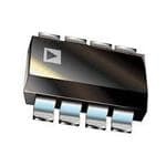
| 描述 | IC POT DGTL 5K 256POS SOT23-8数字电位计 IC IC 256-pos I2C |
| DevelopmentKit | EVAL-AD5245EBZ |
| 产品分类 | |
| 品牌 | Analog Devices |
| 产品手册 | |
| 产品图片 |
|
| rohs | 符合RoHS无铅 / 符合限制有害物质指令(RoHS)规范要求 |
| 产品系列 | 数字电位计 IC,Analog Devices AD5245BRJZ5-RL7- |
| 数据手册 | |
| 产品型号 | AD5245BRJZ5-RL7 |
| POT数量 | Single |
| 产品目录页面 | |
| 产品种类 | 数字电位计 IC |
| 供应商器件封装 | SOT-23-8 |
| 其它名称 | AD5245BRJZ5-RL7CT |
| 包装 | 剪切带 (CT) |
| 商标 | Analog Devices |
| 存储器类型 | 易失 |
| 安装类型 | 表面贴装 |
| 安装风格 | SMD/SMT |
| 容差 | 30 % |
| 封装 | Reel |
| 封装/外壳 | SOT-23-8 |
| 封装/箱体 | SOT-23-8 |
| 工作温度 | -40°C ~ 125°C |
| 工作电源电压 | 5.5 V |
| 工厂包装数量 | 3000 |
| 弧刷存储器 | Volatile |
| 抽头 | 256 |
| 接口 | I²C(设备位址) |
| 描述/功能 | 256 Position I2C Compatible Digital Potentiometer |
| 数字接口 | I2C |
| 最大工作温度 | + 125 C |
| 最小工作温度 | - 40 C |
| 标准包装 | 1 |
| 每POT分接头 | 256 |
| 温度系数 | 35 PPM / C |
| 电压-电源 | 2.7 V ~ 5.5 V |
| 电源电压-最大 | 5.5 V |
| 电源电压-最小 | 2.7 V |
| 电源电流 | 3 uA |
| 电路数 | 1 |
| 电阻 | 5 kOhms |
| 电阻(Ω) | 5k |
| 系列 | AD5245 |


- 商务部:美国ITC正式对集成电路等产品启动337调查
- 曝三星4nm工艺存在良率问题 高通将骁龙8 Gen1或转产台积电
- 太阳诱电将投资9.5亿元在常州建新厂生产MLCC 预计2023年完工
- 英特尔发布欧洲新工厂建设计划 深化IDM 2.0 战略
- 台积电先进制程称霸业界 有大客户加持明年业绩稳了
- 达到5530亿美元!SIA预计今年全球半导体销售额将创下新高
- 英特尔拟将自动驾驶子公司Mobileye上市 估值或超500亿美元
- 三星加码芯片和SET,合并消费电子和移动部门,撤换高东真等 CEO
- 三星电子宣布重大人事变动 还合并消费电子和移动部门
- 海关总署:前11个月进口集成电路产品价值2.52万亿元 增长14.8%


PDF Datasheet 数据手册内容提取
256-Position I2C®-Compatible Digital Potentiometer AD5245 FEATURES FUNCTIONAL BLOCK DIAGRAM 256-position VDD End-to-end resistance 5 kΩ, 10 kΩ, 50 kΩ, 100 kΩ Compact SOT-23-8 (2.9 mm × 3 mm) package A SCL I2CINTERFACE Fast settling time: t = 5 µs typ on power-up S SDA Full read/write of wiper register AD0 W Power-on preset to midscale Extra package address decode pin AD0 WIPER B Computer software replaces µC in factory programming REGISTER applications POR SLoinwg ltee msuppeprlayt:u 2r.e7 cVo teoff 5ic.5ie Vn t 45 ppm/°C GND 03436-001 Figure 1. Low power: I = 8 µA DD Wide operating temperature: –40°C to +125°C Evaluation board available PIN CONFIGURATION APPLICATIONS W 1 8 A Mechanical potentiometer replacement in new designs VDD 2 AD5245 7 B LLCCDD ppaanneell VbrCOigMh atdnjeussst manedn ct ontrast control GSNCDL 34 (NToOt Pto V SIEcWale) 56 ASDDA0 03436-002 Transducer adjustment of pressure, temperature, position, Figure 2. chemical, and optical sensors RF amplifier biasing Automotive electronics adjustment Gain control and offset adjustment GENERAL DESCRIPTION The AD5245 provides a compact 2.9 mm × 3 mm packaged Operating from a 2.7 V to 5.5 V power supply and consuming solution for 256-position adjustment applications. These less than 8 µA allows usage in portable battery-operated devices perform the same electronic adjustment function as applications. mechanical potentiometers or variable resistors, with enhanced Note that the terms digital potentiometer, VR, and RDAC are resolution, solid-state reliability, and superior low temperature used interchangeably. coefficient performance. The wiper settings are controllable through an I2C-compatible digital interface, which can also be used to read back the wiper register content. AD0 can be used to place up to two devices on the same bus. Command bits are available to reset the wiper position to midscale or to shut down the device into a state of zero power consumption. Rev. B Information furnished by Analog Devices is believed to be accurate and reliable. However, no responsibility is assumed by Analog Devices for its use, nor for any infringements of patents or other One Technology Way, P.O. Box 9106, Norwood, MA 02062-9106, U.S.A. rights of third parties that may result from its use. Specifications subject to change without notice. No license is granted by implication or otherwise under any patent or patent rights of Analog Devices. Tel: 781.329.4700 www.analog.com Trademarks and registered trademarks are the property of their respective owners. Fax: 781.461.3113 ©2006 Analog Devices, Inc. All rights reserved.
AD5245 TABLE OF CONTENTS Features..............................................................................................1 Test Circuits.....................................................................................12 Applications.......................................................................................1 Theory of Operation......................................................................13 Functional Block Diagram..............................................................1 Programming the Variable Resistor.........................................13 Pin Configuration.............................................................................1 Programming the Potentiometer Divider...............................14 General Description.........................................................................1 ESD Protection...........................................................................14 Revision History...............................................................................2 Terminal Voltage Operating Range.........................................14 Electrical Characteristics.................................................................3 Power-Up Sequence...................................................................14 5 kΩ Version..................................................................................3 Layout and Power Supply Bypassing.......................................14 10 kΩ, 50 kΩ, 100 kΩ Versions..................................................4 Constant Bias to Retain Resistance Setting.............................15 Timing Characteristics.....................................................................5 Evaluation Board........................................................................15 5 kΩ, 10 kΩ, 50 kΩ, 100 kΩ Versions........................................5 I2C Interface....................................................................................16 Absolute Maximum Ratings............................................................6 I2C-Compatible 2-Wire Serial Bus...........................................16 ESD Caution..................................................................................6 Outline Dimensions.......................................................................19 Pin Configuration and Function Descriptions.............................7 Ordering Guide..........................................................................19 Typical Performance Characteristics.............................................8 REVISION HISTORY Added Figure 37............................................................................14 1/06—Rev. A to Rev. B Changes to Equation 4..................................................................14 Changes to Table 3...........................................................................5 Deleted Readback RDAC Value Section....................................14 Changes to Ordering Guide.........................................................19 Deleted Level Shifting for Bidirectional Interface Section......14 3/04—Rev. 0 to Rev. A Moved ESD Protection Section to Page.....................................14 Updated Format................................................................Universal Changes to Figure 38 and Figure 39............................................14 Changes to Features.........................................................................1 Moved Terminal Voltage Operating Range Section to Page....14 Changes to Applications.................................................................1 Changes to Figure 40.....................................................................14 Changes to Figure 1.........................................................................1 Moved Power-Up Sequence Section to Page.............................14 Changes to Electrical Characteristics—5 kΩ Version................3 Moved Layout and Power Supply Bypassing Section to Page.15 Changes to Electrical Characteristics—10 kΩ, 50 kΩ, Added Constant Bias to Retain Resistance Setting Section.....15 and 100 kΩ Versions.......................................................................4 Added Figure 42............................................................................15 Changes to Timing Characteristics...............................................5 Added Evaluation Board Section................................................15 Changes to Absolute Maximum Ratings......................................6 Added Figure 43............................................................................15 Moved ESD Caution to Page..........................................................6 Moved I2C Interface Section to Page...........................................16 Changes to Pin Configuration and Function Descriptions.......7 Changes to I2C Compatible 2-Wire Serial Bus Section...........16 Changes to Figures 22 and 23......................................................11 Moved Table 5 and Table 6 to Page.............................................17 Moved Figure 25 to Figure 26......................................................11 (Renumbered as Table 8 and Table 9) Moved Figure 26 to Figure 27......................................................11 Moved Figure 36, Figure 37, and Figure 38 to Page..................17 Moved Figure 27 to Figure 25......................................................11 (Renumbered as Figure 44, Figure 45, and Figure 46) Deleted Figures 31 and 32............................................................12 Moved Multiply Devices on One Bus Section to Page.............18 Changes to Figure 32, Figure 33 and Figure 34.........................12 Updated Ordering Guide.............................................................19 Changes to Rheostat Operation Section.....................................13 Updated Outline Dimensions......................................................19 Added Figure 35.............................................................................13 Moved I2C Disclaimer to Page.....................................................20 Changes to Equation 1 and Equation 2......................................13 5/03—Revision 0: Initial Version Changes to Table 6 and Table 7....................................................13 Rev. B | Page 2 of 20
AD5245 ELECTRICAL CHARACTERISTICS 5 kΩ VERSION V = 5 V ± 10% or 3 V ± 10%, V = V , V = 0 V, –40°C < T < +125°C, unless otherwise noted. DD A DD B A Table 1. Parameter Symbol Conditions Min Typ1 Max Unit DC CHARACTERISTICS—RHEOSTAT MODE Resistor Differential Nonlinearity2 R-DNL R , V = no connect –1.5 ±0.1 +1.5 LSB WB A Resistor Integral Nonlinearity2 R-INL R , V = no connect –4 ±0.75 +4 LSB WB A Nominal Resistor Tolerance3 ∆R T = 25°C –30 +30 % AB A Resistance Temperature Coefficient (∆R /R )/∆T × 106 V = V , wiper = no connect 45 ppm/°C AB AB AB DD Wiper Resistance R 50 120 Ω W DC CHARACTERISTICS—POTENTIOMETER DIVIDER MODE (Specifications Apply to All VRs) Differential Nonlinearity4 DNL –1.5 ±0.1 +1.5 LSB Integral Nonlinearity4 INL –1.5 ±0.6 +1.5 LSB Voltage Divider Temperature Coefficient (∆V /V )/∆T × 106 Code = 0x80 15 ppm/°C W W Full-Scale Error V Code = 0xFF –6 –2.5 0 LSB WFSE Zero-Scale Error V Code = 0x00 0 2 6 LSB WZSE RESISTOR TERMINALS Voltage Range5 V , V, V GND V V A B W DD f = 1 MHz, measured to GND, Capacitance A, B6 C , C code = 0x80 90 pF A B f = 1 MHz, measured to GND, Capacitance W6 C code = 0x80 95 pF W Shutdown Supply Current7 I V = 5.5 V 0.01 1 µA A_SD DD Common-Mode Leakage I V = V = V /2 1 nA CM A B DD DIGITAL INPUTS AND OUTPUTS Input Logic High V V = 5 V 2.4 V IH DD Input Logic Low V V = 5 V 0.8 V IL DD Input Logic High V V = 3 V 2.1 V IH DD Input Logic Low V V = 3 V 0.6 V IL DD Input Current I V = 0 V or 5 V ±1 µA IL IN Input Capacitance6 C 5 pF IL POWER SUPPLIES Power Supply Range V 2.7 5.5 V DD RANGE Supply Current I V = 5 V or V = 0 V 3 8 µA DD IH IL Power Dissipation8 P V = 5 V or V = 0 V, V = 5 V 44 µW DISS IH IL DD Power Supply Sensitivity PSS V = +5 V ± 10%, code = midscale ±0.02 ±0.05 %/% DD DYNAMIC CHARACTERISTICS6, 9 Bandwidth –3 dB BW_5K R = 5 kΩ, code = 0x80 1.2 MHz AB Total Harmonic Distortion THD V = 1 V rms, V = 0 V, f = 1 kHz 0.1 % W A B V Settling Time t V = 5 V, V = 0 V, ±1 LSB error band 1 µs W S A B Resistor Noise Voltage Density e R = 2.5 kΩ, R = 0 6 nV/√Hz N_WB WB S 1 Typical specifications represent average readings at 25°C and VDD = 5 V. 2 Resistor position nonlinearity error R-INL is the deviation from an ideal value measured between the maximum resistance and the minimum resistance wiper positions. R-DNL measures the relative step change from ideal between successive tap positions. Parts are guaranteed monotonic. 3 VAB = VDD, wiper (VW) = no connect. 4 INL and DNL are measured at VW with the RDAC configured as a potentiometer divider similar to a voltage output D/A converter. VA = VDD and VB = 0 V. DNL specification limits of ±1 LSB maximum are guaranteed monotonic operating conditions. 5 Resistor Terminals A, B, and W have no limitations on polarity with respect to each other. 6 Guaranteed by design and not subject to production test. 7 Measured at the A terminal. The A terminal is open circuited in shutdown mode. 8 PDISS is calculated from (IDD × VDD). CMOS logic level inputs result in minimum power dissipation. 9 All dynamic characteristics use VDD = 5 V. Rev. B | Page 3 of 20
AD5245 10 kΩ, 50 kΩ, 100 kΩ VERSIONS V = 5 V ± 10% or 3 V ± 10%, V = V , V = 0 V, –40°C < T < +125°C, unless otherwise noted. DD A DD B A Table 2. Parameter Symbol Conditions Min Typ1 Max Unit DC CHARACTERISTICS—RHEOSTAT MODE Resistor Differential Nonlinearity2 R-DNL R , V = no connect –1 ±0.1 +1 LSB WB A Resistor Integral Nonlinearity2 R-INL R , V = no connect –2 ±0.25 +2 LSB WB A Nominal Resistor Tolerance3 ∆R T = 25°C –30 +30 % AB A Resistance Temperature Coefficient (∆R /R )/∆T × 106 V = V , wiper = no connect 45 ppm/°C AB AB AB DD Wiper Resistance R V = 5 V 50 120 Ω W DD DC CHARACTERISTICS—POTENTIOMETER DIVIDER MODE (Specifications Apply to All VRs) Differential Nonlinearity4 DNL –1 ±0.1 +1 LSB Integral Nonlinearity4 INL –1 ±0.3 +1 LSB Voltage Divider Temperature Coefficient (∆V /V )/∆T × 106 Code = 0x80 15 ppm/°C W W Full-Scale Error V Code = 0xFF –3 –1 0 LSB WFSE Zero-Scale Error V Code = 0x00 0 1 3 LSB WZSE RESISTOR TERMINALS Voltage Range5 V , V, V GND V V A B W DD Capacitance A, B6 C , C f = 1 MHz, measured to GND, 90 pF A B code = 0x80 Capacitance W6 C f = 1 MHz, measured to GND, 95 pF W code = 0x80 Shutdown Supply Current I V = 5.5 V 0.01 1 µA A_SD DD Common-Mode Leakage I V = V = V /2 1 nA CM A B DD DIGITAL INPUTS AND OUTPUTS Input Logic High V V = 5 V 2.4 V IH DD Input Logic Low V V = 5 V 0.8 V IL DD Input Logic High V V = 3 V 2.1 V IH DD Input Logic Low V V = 3 V 0.6 V IL DD Input Current I V = 0 V or 5 V ±1 µA IL IN Input Capacitance6 C 5 pF IL POWER SUPPLIES Power Supply Range V 2.7 5.5 V DD RANGE Supply Current I V = 5 V or V = 0 V 3 8 µA DD IH IL Power Dissipation7 P V = 5 V or V = 0 V, V = 5 V 44 µW DISS IH IL DD Power Supply Sensitivity PSS V = 5 V ± 10%, ±0.02 ±0.05 %/% DD code = midscale DYNAMIC CHARACTERISTICS6, 8 Bandwidth –3 dB BW R = 10 kΩ/50 kΩ/100 kΩ, 600/100/40 kHz AB code = 0x80 Total Harmonic Distortion THD V = 1 V rms, V = 0 V, f = 1 kHz, 0.1 % W A B R = 10 kΩ AB V Settling Time (10 kΩ/50 kΩ/100 kΩ) t V = 5 V, V = 0 V, 2 µs W S A B ±1 LSB error band Resistor Noise Voltage Density e R = 5 kΩ, R = 0 9 nV/√Hz N_WB WB S 1 Typical specifications represent average readings at 25°C and VDD = 5 V. 2 Resistor position nonlinearity error R-INL is the deviation from an ideal value measured between the maximum resistance and the minimum resistance wiper positions. R-DNL measures the relative step change from ideal between successive tap positions. Parts are guaranteed monotonic. 3 VAB = VDD, wiper (VW) = no connect. 4 INL and DNL are measured at VW with the RDAC configured as a potentiometer divider similar to a voltage output D/A converter. VA = VDD and VB = 0 V. DNL specification limits of ±1 LSB maximum are guaranteed monotonic operating conditions. 5 Resistor Terminals A, B, W have no limitations on polarity with respect to each other. 6 Guaranteed by design and not subject to production test. 7 PDISS is calculated from (IDD × VDD). CMOS logic level inputs result in minimum power dissipation. 8 All dynamic characteristics use VDD = 5 V. Rev. B | Page 4 of 20
AD5245 TIMING CHARACTERISTICS 5 KΩ, 10 KΩ, 50 KΩ, 100 KΩ VERSIONS V = 5 V ± 10% or 3 V ± 10%, V = V , V = 0 V, –40°C < T < +125°C, unless otherwise noted. DD A DD B A Table 3. Parameter Symbol Conditions Min Typ1 Max Unit I2C INTERFACE TIMING CHARACTERISTICS2, 3, 4 (Specifications Apply to All Parts) SCL Clock Frequency f 400 kHz SCL t Bus Free Time Between STOP and START t 1.3 µs BUF 1 t Hold Time (Repeated START) t After this period, the first clock 0.6 µs HD;STA 2 pulse is generated. t Low Period of SCL Clock t 1.3 µs LOW 3 t High Period of SCL Clock t 0.6 µs HIGH 4 t Setup Time for Repeated START Condition t 0.6 µs SU;STA 5 t Data Hold Time t 0.9 µs HD;DAT 6 t Data Setup Time t 100 ns SU;DAT 7 t Fall Time of Both SDA and SCL Signals t 300 ns F 8 t Rise Time of Both SDA and SCL Signals t 300 ns R 9 t Setup Time for STOP Condition t 0.6 µs SU;STO 10 1 Typical specifications represent average readings at 25°C and VDD = 5 V. 2 Guaranteed by design and not subject to production test. 3 See timing diagram (Figure 44) for locations of measured values. 4 Standard I2C mode operation guaranteed by design. Rev. B | Page 5 of 20
AD5245 ABSOLUTE MAXIMUM RATINGS T = 25°C, unless otherwise noted. A Table 4. Stresses above those listed under Absolute Maximum Ratings Parameter Value may cause permanent damage to the device. This is a stress VDD to GND –0.3 V to +7 V rating only; functional operation of the device at these or any VA, VB, VW to GND VDD other conditions above those indicated in the operational Terminal Current, A to B, A to W, B to W1 section of this specification is not implied. Exposure to absolute Pulsed ±20 mA maximum rating conditions for extended periods may affect Continuous ±5 mA device reliability. Digital Inputs and Output Voltage to GND 0 V to 7 V Operating Temperature Range –40°C to +125°C Maximum Junction Temperature (T ) 150°C JMAX Storage Temperature Range –65°C to +150°C Lead Temperature (Soldering, 10 sec) 245°C Thermal Resistance2 θ : SOT-23-8 230°C/W JA 1 Maximum terminal current is bound by the maximum current handling of the switches, maximum power dissipation of the package, and maximum applied voltage across any two of the A, B, and W terminals at a given resistance. 2 Package power dissipation = (TJMAX – TA)/θJA. ESD CAUTION ESD (electrostatic discharge) sensitive device. Electrostatic charges as high as 4000 V readily accumulate on the human body and test equipment and can discharge without detection. Although this product features proprietary ESD protection circuitry, permanent damage may occur on devices subjected to high energy electrostatic discharges. Therefore, proper ESD precautions are recommended to avoid performance degradation or loss of functionality. Rev. B | Page 6 of 20
AD5245 PIN CONFIGURATION AND FUNCTION DESCRIPTIONS W 1 8 A VDD 2 AD5245 7 B GSNCDL 34 (NToOt Pto V SIEcWale) 56 ASDDA0 03436-002 Figure 3. Pin Configuration Table 5. Pin Function Descriptions Pin No. Mnemonic Description 1 W W Terminal. GND ≤ V ≤ V . W DD 2 V Positive Power Supply. DD 3 GND Digital Ground. 4 SCL Serial Clock Input. Positive edge triggered. Pull-up resistor required. 5 SDA Serial Data Input/Output. Pull-up resistor required. 6 AD0 Programmable Address Bit 0 for Two-Device Decoding. 7 B B Terminal. GND ≤ V ≤ V . B DD 8 A A Terminal. GND ≤ V ≤ V . A DD Rev. B | Page 7 of 20
AD5245 TYPICAL PERFORMANCE CHARACTERISTICS 1.0 1.0 –40°C 0.8 5V 0.8 +25°C +85°C 3V +125°C E INL (LSB) 000...246 E DNL (LSB) 000...246 D D O 0 O 0 M M T R RHEOSTA ––00..42 TIOMETE ––00..42 –0.6 EN –0.6 T O –0.8 P –0.8 –1.0 –1.0 0 32 64 96CODE1 2(D8ecim1a6l)0 192 224 256 03436-003 0 32 64 96CODE1 (2D8ecima1l6)0 192 224 256 03436-006 Figure 4. R-INL vs. Code vs. Supply Voltages Figure 7. DNL vs. Code vs. Temperature, VDD = 5 V 1.0 1.0 5V 5V 3V 3V 0.8 0.8 SB) 0.6 SB) 0.6 L L NL ( 0.4 NL ( 0.4 OSTAT MODE D –00.2.02 METER MODE I –00.2.02 E O RH –0.4 NTI –0.4 E –0.6 OT –0.6 P –0.8 –0.8 –1.0 –1.0 0 32 64 96CODE1 2(D8ecim1a6l)0 192 224 256 03436-004 0 32 64 96CODE1 2(D8ecim1a6l)0 192 224 256 03436-007 Figure 5. R-DNL vs. Code vs. Supply Voltages Figure 8. INL vs. Code vs. Supply Voltages 1.0 1.0 –40°C 5V +25°C 0.8 +85°C 0.8 3V +125°C B) B) 0.6 LS 0.6 L (LS 0.4 DNL ( 0.4 DE IN 0.2 ODE 0.2 O M M 0 R 0 R E ETE –0.2 MET –0.2 M O O –0.4 TI –0.4 NTI EN OTE –0.6 POT –0.6 P –0.8 –0.8 –1.0 –1.0 0 32 64 96CODE1 (2D8ecima1l6)0 192 224 256 03436-005 0 32 64 96CODE12 (8Decim1a6l0) 192 224 256 03436-008 Figure 6. INL vs. Code vs. Temperature, VDD = 5 V Figure 9. DNL vs. Code vs. Supply Voltages Rev. B | Page 8 of 20
AD5245 1.0 –40°C 2.5 +25°C 0.8 +85°C +125°C NL (LSB) 00..46 OR (µA) 2.0 DE I 0.2 ERR 1.5 RHEOSTAT MO ––00..420 E, ZERO-SCALE 1.0 VDD = 2.7V VDD = 5.5V –0.6 ZS 0.5 –0.8 –1.0 0 0 32 64 96CODE1 2(D8ecim1a6l)0 192 224 256 03436-009 ––4400 00 TEMPE44R00ATURE (°C) 8800 112200 03436-012 Figure 10. R-INL vs. Code vs. Temperature, VDD = 5 V Figure 13. Zero-Scale Error vs. Temperature 1.0 –40°C 10 +25°C 0.8 +85°C SB) 0.6 +125°C L ODE DNL ( 00..24 RENT (µA) VDD = 5.5V STAT M –0.20 LY CUR 1 O P RHE –0.4 SUP D –0.6 ID VDD = 2.7V –0.8 –1.0 0 32 64 96CODE1 2(D8ecim1a6l)0 192 224 256 03436-010 0.1–40 0 TEMPERA4T0URE (°C) 80 120 03436-013 Figure 11. R-DNL vs. Code vs. Temperature, VDD = 5 V Figure 14. Supply Current vs. Temperature 2.5 70 B) 2.0 60 LS A) OR ( VDD = 2.7V T (n 50 RR 1.5 EN E R L-SCALE 1.0 VDD = 5.5V OWN CUR 3400 L D FU UT VDD = 5V FSE, 0.5 ISHA 20 10 0 ––4400 Figure 1002. Full-ScTaElMe 44PE00ErrRoAr TvUs.R TEe m(°C88p)00erature 112200 03436-011 0–40 0 TEMPE4R0ATURE (°C)80 120 03436-014 Figure 15. Shutdown Current vs. Temperature Rev. B | Page 9 of 20
AD5245 REF LEVEL /DIV MARKER 510 634.725Hz 200 0.000dB 6.000dB MAG (A/R) –9.049dB 0 C) –6 0x80 m/° 150 p –12 0x40 p CO ( –18 0x20 P 100 M 0x10 E –24 T E 0x08 MOD 50 –30 0x04 AT –36 0x02 T OS –42 0x01 E 0 H R –48 –54 –50 0 32 64 9C6ODE 1(D2e8cima1l)60 192 224 256 03436-015 –6S0TA1RkT 1 000.000Hz 1 0 k 1 0S0TkOP 1 000 000.0001HMz 03436-018 Figure 16. Rheostat Mode Tempco ∆RWB/∆T vs. Code Figure 19. Gain vs. Frequency vs. Code, RAB = 10 kΩ REF LEVEL /DIV MARKER 100 885.289Hz 160 0.000dB 6.000dB MAG (A/R) –9.014dB m/°C) 140 –06 0x80 p O (p 120 –12 0x40 C MP 100 –18 0x20 E E T 80 –24 0x10 D MO 60 –30 0x08 R E 0x04 T 40 –36 E M 0x02 NTIO 20 –42 0x01 OTE 0 –48 P –54 –20 0 32 64 96CODE1 2(D8ecim1a6l)0 192 224 256 03436-016 –6S0TA1RkT 1 000.000Hz 1 0 k 1 0S0TkOP 1 000 000.0001HMz 03436-019 Figure 17. Potentiometer Mode Tempco ∆VWB/∆T vs. Code Figure 20. Gain vs. Frequency vs. Code, RAB = 50 kΩ REF LEVEL /DIV MARKER 54 089.173Hz REF LEVEL /DIV MARKER 1 000 000.000Hz 0.000dB 6.000dB MAG (A/R) –9.052dB 0.000dB 6.000dB MAG (A/R) –8.918dB 0 0 0x80 –6 0x80 –6 –12 0x40 –12 0x40 –18 0x20 –18 0x20 0x10 –24 0x10 –24 0x08 –30 0x08 –30 –36 00xx0042 –36 0x04 0x01 –42 0x02 –42 0x01 –48 –48 –54 –54 –60 –6S0T1AkRT 1 000.000Hz 1 0 k 1 0 S0TkOP 1 000 000.0001HMz 03436-017 STA1kRT 1 000.000Hz 1 0 k 1 0 0SkTOP 1 000 000.0001HMz 03436-020 Figure 18. Gain vs. Frequency vs. Code, RAB = 5 kΩ Figure 21. Gain vs. Frequency vs. Code, RAB = 100 kΩ Rev. B | Page 10 of 20
AD5245 REF LEVEL /DIV –5.000dB 0.500dB –5.5 5kΩ– 1.026MHz –6.0 10kΩ– 511kHz 50kΩ– 101kHz –6.5 100kΩ– 54kHz –7.0 –7.5 –8.0 1 VW –8.5 R = 50kΩ R = 5kΩ –9.0 SCL R = 100kΩ R = 10kΩ –9.5 2 ––1100..05 Ch 1 200mV BW Ch 2 5.00 V BWM 100ns A CH2 3.00 V 03436-024 ST1A0kRT 1 000.000Hz 1 0 0 k S1MTOP 1 000 000.00100HMz 03436-021 Figure 22. –3 dB Bandwidth @ Code = 0x80 Figure 25. Large Signal Settling Time, Code 0xFF ≥ 0x00 60 CODE = 0x80, VA= VDD, VB = 0V VA = 5V VB = 0V 40 B) d – R ( PSRR @ VDD = 3V DC±10% p-pAC R 1 VW S P 20 SCL 2 0100 PSRR @ V1DkD = 5V FDRCE±Q10U1%E0N kpC-pY A(HCz) 100k 1M 03436-022 Ch 1 100mV BFWigurCeh 2 26 .5 D.0i0g iVtalB FWeeMd t2h0r0onusg hA CH1 152mV 03436-025 Figure 23. PSRR vs. Frequency 900 VDD= 5V 800 700 VA = 5V VB = 0V 600 500 A) µ CODE = 0x55 1 VW (D 400 D I 300 CODE = 0xFF SCL 200 2 101000k 100k FREQUENCY (H1zM) 10M 03436-023 Ch 1 5.00V BW Ch 2 5.00 V BWM 200ns A CH1 3.00 V 03436-026 Figure 24. IDD vs. Frequency Figure 27. Midscale Glitch, Code 0x80 ≥ 0x7F Rev. B | Page 11 of 20
AD5245 TEST CIRCUITS Figure 28 to Figure 34 illustrate the test circuits that define the test conditions used in the product specification tables (Table 1 through Table 3). ADUT V1L+S =B V =D DV+/2N A DWUT +15V V+ W VIN AD8610 B VOUT B VMS 03436-027 OFFGSNEDT 2.5V –15V 03436-031 Figure 28. Test Circuit for Potentiometer Divider Nonlinearity Error Figure 32. Test Circuit for Gain vs. Frequency (INL, DNL) NO CONNECT 0.1V DUT DUT RSW= ISW A W IW CODE = 0x00 W B B ISW 0.1V VMS 03436-028 GNDTO VDD 03436-032 Figure 29. Test Circuit for Resistor Position Nonlinearity Error Figure 33. Test Circuit for Incremental On Resistance (Rheostat Operation; R-INL, R-DNL) NC DUT A IW = VDD/RNOMINAL DUT VMS2 W VW VDD A W ICM B VMS1 RW = [VMS1 – VMS2]/IW 03436-029 GND NCB NC = NO CONNECT VCM 03436-033 Figure 34. Test Circuit for Common-Mode Leakage Current Figure 30. Test Circuit for Wiper Resistance VA V+ = VDD±10% ( ∆ V M S ) PSRR (dB) = 20log V+ VDD A W PSS (%/%) =∆VMS%∆VDD ∆VDD% B VMS 03436-030 Figure 31. Test Circuit for Power Supply Sensitivity (PSS, PSSR) Rev. B | Page 12 of 20
AD5245 THEORY OF OPERATION The AD5245 is a 256-position digitally controlled variable The general equation determining the digitally programmed resistor (VR) device. output resistance between W and B is D An internal power-on preset places the wiper at midscale R (D)= ×R +2×R (1) WB AB W during power-on, which simplifies the fault condition recovery 256 at power-up. where: PROGRAMMING THE VARIABLE RESISTOR D is the decimal equivalent of the binary code loaded in the 8-bit RDAC register. Rheostat Operation RAB is the end-to-end resistance. The nominal resistance of the RDAC between Terminals A and RW is the wiper resistance contributed by the on resistance of B is available in 5 kΩ, 10 kΩ, 50 kΩ, and 100 kΩ. The nominal the internal switch. resistance (R ) of the VR has 256 contact points accessed by AB the wiper terminal, plus the B terminal contact. The 8-bit data In summary, if RAB = 10 kΩ and the A terminal is open in the RDAC latch is decoded to select one of the 256 possible circuited, then the following output resistance RWB is set for the settings. indicated RDAC latch codes. Table 6. Codes and Corresponding R Resistance WB A A A D (Dec.) R (Ω) Output State WB W W W 255 9,961 Full Scale (R – 1 LSB + R ) AB W B B B 03436-034 112 8 51,3096 0 M1 LidSsBc ale Figure 35. Rheostat Mode Configuration 0 100 Zero Scale (Wiper Contact Resistance) Assuming that a 10 kΩ part is used, the wiper’s first connection Note that in the zero-scale condition, a finite wiper resistance of starts at the B terminal for Data 0x00. Because there is a 50 Ω 100 Ω is present. Care should be taken to limit the current flow wiper contact resistance, such a connection yields a minimum between W and B in this state to a maximum pulse current of of 100 Ω (2 × 50 Ω) resistance between Terminals W and B. The no more than 20 mA. Otherwise, degradation or possible second connection is the first tap point, which corresponds to destruction of the internal switch contact can occur. 139 Ω (R = R /256 + 2 × R = 39 Ω + 2 × 50 Ω) for Data 0x01. WB AB W Similar to the mechanical potentiometer, the resistance of the The third connection is the next tap point, representing 178 Ω RDAC between the Wiper W and Terminal A also produces a (2 × 39 Ω + 2 × 50 Ω) for Data 0x02, and so on. Each LSB data digitally controlled complementary resistance, R . When these WA value increase moves the wiper up the resistor ladder until the terminals are used, the B terminal can be opened. Setting the last tap point is reached at 10,100 Ω (R + 2 × R ). AB W resistance value for R starts at a maximum value of resistance WA and decreases as the data loaded in the latch increases in value. A RS The general equation for this operation is 256−D R (D)= ×R +2×R (2) WA AB W D7 RS 256 D6 D5 D4 For R = 10 kΩ and the B terminal open circuited, the D3 RS AB D2 following output resistance R is set for the indicated RDAC D1 WA D0 W latch codes. Table 7. Codes and Corresponding R Resistance WA D (Dec.) R (Ω) Output State WA 255 139 Full Scale RDAC RS 128 5,060 Midscale LATCH 1 9,961 1 LSB AND B DECODER 0 10,060 Zero Scale 03436-035 Typical device-to-device matching is process lot dependent and Figure 36. AD5245 Equivalent RDAC Circuit can vary by up to ±30%. Because the resistance element is processed in thin film technology, the change in R with AB temperature has a very low 45 ppm/°C temperature coefficient. Rev. B | Page 13 of 20
AD5245 PROGRAMMING THE POTENTIOMETER DIVIDER TERMINAL VOLTAGE OPERATING RANGE Voltage Output Operation The AD5245 V and GND power supply defines the boundary DD The digital potentiometer easily generates a voltage divider at conditions for proper 3-terminal digital potentiometer wiper-to-B and wiper-to-A proportional to the input voltage at operation. Supply signals present on Terminals A, B, and W that A to B. Unlike the polarity of VDD to GND, which must be exceed VDD or GND are clamped by the internal forward-biased positive, voltage across A to B, W to A, and W to B can be at diodes (see Figure 40). either polarity. VDD A VI A W W B VO B 03436-036 Figure 40. Maximum Terminal Voltages SGeNt Dby V03436-039D D and GND Figure 37. Potentiometer Mode Configuration POWER-UP SEQUENCE If ignoring the effect of the wiper resistance for approximation, Because the ESD protection diodes limit the voltage compliance then connecting the A terminal to 5 V and the B terminal to at Terminals A, B, and W (see Figure 40), it is important to ground produces an output voltage at the wiper-to-B starting at power V and GND before applying any voltage to Terminals DD 0 V up to 1 LSB less than 5 V. Each LSB of voltage is equal to the A, B, and W; otherwise, the diode is forward biased such that voltage applied across Terminal A and B divided by the 256 V is powered unintentionally and can affect the rest of the DD positions of the potentiometer divider. The general equation user’s circuit. The ideal power-up sequence is in the following defining the output voltage at V with respect to ground for any W order: GND, V , digital inputs, and then V , V , and V . The DD A B W valid input voltage applied to Terminals A and B is relative order of powering V , V , V , and the digital inputs is A B W V (D)= D V +256−DV (3) not important as long as they are powered after VDD and GND. W A B 256 256 LAYOUT AND POWER SUPPLY BYPASSING A more accurate calculation, which includes the effect of wiper It is good practice to employ compact, minimum lead length resistance, V , is W layout design. The leads to the inputs should be as direct as R (D) R (D) possible with a minimum conductor length. Ground paths V (D)= WB V + WA V (4) W R A R B should have low resistance and low inductance. AB AB Similarly, it is also good practice to bypass the power supplies Operation of the digital potentiometer in the divider mode with quality capacitors for optimum stability. Supply leads to results in a more accurate operation over temperature. Unlike the device should be bypassed with disk or chip ceramic the rheostat mode, the output voltage is dependent mainly on capacitors of 0.01 µF to 0.1 µF. Low ESR 1 µF to 10 µF tantalum the ratio of the internal resistors, R and R , not the absolute WA WB or electrolytic capacitors should also be applied at the supplies values. Therefore, the temperature drift reduces to 15 ppm/°C. to minimize any transient disturbance and low frequency ripple ESD PROTECTION (see Figure 41). Note that the digital ground should also be joined remotely to the analog ground at one point to minimize All digital inputs are protected with a series of input resistors and the ground bounce. parallel Zener ESD structures, shown in Figure 38 and Figure 39. This applies to the digital input pins SDA, SCL, and AD0. 340Ω LOGIC VDD C3 + C1 VDD GND 03436-037 10µF 0.1µF AD5245 Figure 38. ESD Protection of Digital Pins A, B, W GND GND 03436-038 Figure 41. Power Supply Bypassing 03436-040 Figure 39. ESD Protection of Resistor Terminals Rev. B | Page 14 of 20
AD5245 CONSTANT BIAS TO RETAIN RESISTANCE SETTING Although the resistance setting of the AD5245 is lost when the battery needs replacement, such events occur rather infrequently For users who desire nonvolatility but cannot justify the so that this inconvenience is justified by the lower cost and additional cost for the EEMEM, the AD5245 can be considered smaller size offered by the AD5245. If total power is lost, then a low cost alternative by maintaining a constant bias to retain the user should be provided with a means to adjust the setting the wiper setting. The AD5245 is designed specifically with low accordingly. power in mind, which allows low power consumption even in battery-operated systems. Figure 42 demonstrates the power EVALUATION BOARD consumption from a 3.4 V, 450 mA-hr Li-Ion cell phone battery An evaluation board, along with all necessary software, is that is connected to the AD5245. The measurement over time available to program the AD5245 from any PC running shows that the device draws approximately 1.3 µA and Windows® 98/2000/XP. The graphical user interface, as shown consumes negligible power. Over a course of 30 days, the in Figure 43, is straightforward and easy to use. More detailed battery is depleted by less than 2%, the majority of which is due information is available in the user manual, which is provided to the intrinsic leakage current of the battery itself. with the board. 110% TA= 25°C 108% 106% D E104% T E PL102% E D E 100% F Y LI 98% R E T 96% T A B 9924%% 03436-042 Figure 43. AD5245 Evaluation Board Software 90%0 5 10 DA1Y5S 20 25 30 03436-041 The AD5245 starts at midscale upon power-up. To increment or Figure 42. Battery Operating Life Depletion decrement the resistance, the user can simply move the scroll- bars on the left. To write a specific value, the user should use the This demonstrates that constantly biasing the potentiometer bit pattern in the upper screen and click the Run button. The can be a practical approach. Most portable devices do not format of writing data to the device is shown in Table 8. To read require the removal of batteries for charging. the data from the device, the user can simply click the Read button. The format of the read bits is shown in Table 9. Rev. B | Page 15 of 20
AD5245 I2C INTERFACE I2C-COMPATIBLE 2-WIRE SERIAL BUS 3. After acknowledging the instruction byte, the last byte in The 2-wire I2C serial bus protocol operates as follows: write mode is the data byte. Data is transmitted over the serial bus in sequences of nine clock pulses (eight data bits 1. The master initiates data transfer by establishing a START followed by an acknowledge bit). The transitions on the condition, which is when a high-to-low transition on the SDA SDA line must occur during the low period of SCL and line occurs while SCL is high (see Figure 45). The next byte remain stable during the high period of SCL (see Figure 45). is the slave address byte, which consists of the 7-bit slave 4. In read mode, the data byte follows immediately after the address followed by an R/W bit (this bit determines whether acknowledgment of the slave address byte. Data is data is read from or written to the slave device). The AD5245 transmitted over the serial bus in sequences of nine clock has one configurable address bit, AD0 (see Table 8). pulses (a slight difference with write mode, in which eight data bits are followed by an acknowledge bit). Similarly, the The slave whose address corresponds to the transmitted transitions on the SDA line must occur during the low address responds by pulling the SDA line low during the period of SCL and remain stable during the high period of ninth clock pulse (this is termed the acknowledge bit). At SCL (see Figure 46). this stage, all other devices on the bus remain idle while the selected device waits for data to be written to or read from 5. After all data bits have been read or written, a STOP its serial register. If the R/W bit is high, the master reads condition is established by the master. A STOP condition is from the slave device. On the other hand, if the R/W bit is defined as a low-to-high transition on the SDA line while low, the master writes to the slave device. SCL is high. In write mode, the master pulls the SDA line high during the 10th clock pulse to establish a STOP 2. In write mode, the second byte is the instruction byte. condition (see Figure 45). In read mode, the master issues a The first bit (MSB) of the instruction byte is a don’t care. no acknowledge for the ninth clock pulse (that is, the SDA line remains high). The master then brings the SDA line low The second MSB, RS, is the midscale reset. A logic high on before the 10th clock pulse, which goes high to establish a this bit moves the wiper to the center tap, where R = R . WA WB STOP condition (see Figure 46). This feature effectively overwrites the contents of the register; therefore, when taken out of reset mode, the RDAC A repeated write function gives the user flexibility to update remains at midscale. the RDAC output a number of times after addressing and instructing the part only once. For example, after the RDAC The third MSB, SD, is a shutdown bit. A logic high causes an has acknowledged its slave address and instruction bytes in open circuit at Terminal A while shorting the wiper to the write mode, the RDAC output updates on each successive Terminal B. This operation yields almost 0 Ω in rheostat mode byte. If different instructions are needed, then the write/read or 0 V in potentiometer mode. It is important to note that mode has to start again with a new slave address, instruction, the shutdown operation does not disturb the contents of the and data byte. Similarly, a repeated read function of the register. When brought out of shutdown, the previous setting is RDAC is also allowed. applied to the RDAC. Also during shutdown, new settings can be programmed. When the part is returned from shutdown, the corresponding VR setting is applied to the RDAC. The remainder of the bits in the instruction byte are don’t cares (see Table 8). Rev. B | Page 16 of 20
AD5245 Table 8. Write Mode S 0 1 0 1 1 0 AD0 W A X RS SD X X X X X A D7 D6 D5 D4 D3 D2 D1 D0 A P Slave Address Byte Instruction Byte Data Byte Table 9. Read Mode S 0 1 0 1 1 0 AD0 R A D7 D6 D5 D4 D3 D2 D1 D0 A P Slave Address Byte Data Byte S = START condition R = Read P = STOP condition RS = Reset wiper to midscale 0x80 A = Acknowledge SD = Shutdown connects wiper to B terminal and open circuits X = Don’t care A terminal, but does not change contents of wiper register W = Write D7, D6, D5, D4, D3, D2, D1, D0 = Data Bits t t t 2 8 9 SCL t 6 t2 t3 t4 t7 t5 t10 t 9 t 8 SDA t P 1 S S P 03436-043 Figure 44. I2C Interface Detailed Timing Diagram 1 9 1 9 1 9 SCL SDA 0 1 0 1 1 0 AD0 R/W X RS SD X X X X X D7 D6 D5 D4 D3 D2 D1 D0 ACK BY ACK BY ACK BY AD5245 AD5245 AD5245 SMTAASRTTE BRY SLAVEFARDADMREES 1S BYTE INSTRFURCATMIOEN 2 BYTE DFARTAA MBEY T3E SMTAOSPT EBRY 03436-044 Figure 45. Writing to the RDAC Register 1 9 1 9 SCL SDA 0 1 0 1 1 0 AD0 R/W D7 D6 D5 D4 D3 D2 D1 D0 ACK BY NOACK SMTAASRTTE BRY SLAVEAFRDADMREES 1S BYTE AD5245 RDAFCR RAEMGEI S2TER BY MASTSMETRAOSPT EBRY 03436-045 Figure 46. Reading Data from a Previously Selected RDAC Register in Write Mode Rev. B | Page 17 of 20
AD5245 +5V Multiple Devices on One Bus Figure 47 shows two AD5245 devices on the same serial bus. RP RP Each has a different slave address because the states of their AD0 pins are different. This allows the RDAC within each SDA device to be written to or read from independently. The master MASTER device’s output bus line drivers are open-drain pull-downs in a SCL +5V fully I2C-compatible interface. SDA SCL SDA SCL AADD05245 AADD05245 03436-046 Figure 47. Multiple AD5245 Devices on One I2C Bus Rev. B | Page 18 of 20
AD5245 OUTLINE DIMENSIONS 2.90 BSC 8 7 6 5 1.60 BSC 2.80 BSC 1 2 3 4 PIN1 INDICATOR 0.65 BSC 1.95 1.30 BSC 1.15 0.90 1.45 MAX 0.22 0.08 0.60 0.15 MAX 00..3282 SEATING 84°° 00..4350 PLANE 0° COMPLIANT TO JEDEC STANDARDS MO-178-BA Figure 48. 8-Lead Small Outline Transistor Package [SOT-23] (RJ-8) Dimensions shown in millimeters ORDERING GUIDE Model Temperature Range Package Description Package Option Branding R (Ω) Ordering Quantity AB AD5245BRJ5-R2 –40°C to +125°C 8-Lead SOT-23 RJ-8 D0G 5 k 250 AD5245BRJ5-RL7 –40°C to +125°C 8-Lead SOT-23 RJ-8 D0G 5 k 3,000 AD5245BRJZ5-R21 –40°C to +125°C 8-Lead SOT-23 RJ-8 D0G 5 k 250 AD5245BRJZ5-RL71 –40°C to +125°C 8-Lead SOT-23 RJ-8 D0G 5 k 3,000 AD5245BRJ10-R2 –40°C to +125°C 8-Lead SOT-23 RJ-8 D0H 10 k 250 AD5245BRJ10-RL7 –40°C to +125°C 8-Lead SOT-23 RJ-8 D0H 10 k 3,000 AD5245BRJZ10-R21 –40°C to +125°C 8-Lead SOT-23 RJ-8 D0H 10 k 250 AD5245BRJZ10-RL71 –40°C to +125°C 8-Lead SOT-23 RJ-8 D0H 10 k 3,000 AD5245BRJ50-R2 –40°C to +125°C 8-Lead SOT-23 RJ-8 D0J 50 k 250 AD5245BRJ50-RL7 –40°C to +125°C 8-Lead SOT-23 RJ-8 D0J 50 k 3,000 AD5245BRJZ50-R21 –40°C to +125°C 8-Lead SOT-23 RJ-8 D0J 50 k 250 AD5245BRJZ50-RL71 –40°C to +125°C 8-Lead SOT-23 RJ-8 D0J 50 k 3,000 AD5245BRJ100-R2 –40°C to +125°C 8-Lead SOT-23 RJ-8 D0K 100 k 250 AD5245BRJ100-RL7 –40°C to +125°C 8-Lead SOT-23 RJ-8 D0K 100 k 3,000 AD5245BRJZ100-R21 –40°C to +125°C 8-Lead SOT-23 RJ-8 D0K 100 k 250 AD5245BRJZ100-RL71 –40°C to +125°C 8-Lead SOT-23 RJ-8 D0K 100 k 3,000 AD5245EVAL2 Evaluation Board 1 Z = Pb-free part. 2 The evaluation board is shipped with the 10 kΩ RAB resistor option; however, the board is compatible with all available resistor value options. Rev. B | Page 19 of 20
AD5245 NOTES Purchase of licensed I2C components of Analog Devices or one of its sublicensed Associated Companies conveys a license for the purchaser under the Philips I2C Patent Rights to use these components in an I2C system, provided that the system conforms to the I2C Standard Specification as defined by Philips. ©2006 Analog Devices, Inc. All rights reserved. Trademarks and registered trademarks are the property of their respective owners. C03436-0-1/06(B) Rev. B | Page 20 of 20
Mouser Electronics Authorized Distributor Click to View Pricing, Inventory, Delivery & Lifecycle Information: A nalog Devices Inc.: AD5245BRJZ100-R2 AD5245BRJZ100-RL7 AD5245BRJZ10-R2 AD5245BRJZ10-RL7 AD5245BRJZ50-R2 AD5245BRJZ50-RL7 AD5245BRJZ5-R2 AD5245BRJZ5-RL7 EVAL-AD5245DBZ