ICGOO在线商城 > 传感器,变送器 > 温度传感器 - 温控器 - 固态 > AD22105ARZ
- 型号: AD22105ARZ
- 制造商: Analog
- 库位|库存: xxxx|xxxx
- 要求:
| 数量阶梯 | 香港交货 | 国内含税 |
| +xxxx | $xxxx | ¥xxxx |
查看当月历史价格
查看今年历史价格
AD22105ARZ产品简介:
ICGOO电子元器件商城为您提供AD22105ARZ由Analog设计生产,在icgoo商城现货销售,并且可以通过原厂、代理商等渠道进行代购。 AD22105ARZ价格参考¥14.30-¥14.30。AnalogAD22105ARZ封装/规格:温度传感器 - 温控器 - 固态, Thermostat Programmable Active High Open Collector 8-SOIC。您可以下载AD22105ARZ参考资料、Datasheet数据手册功能说明书,资料中有AD22105ARZ 详细功能的应用电路图电压和使用方法及教程。
AD22105ARZ 是由 Analog Devices Inc. 生产的一款温度传感器,属于温控器 - 固态类别。该型号的温度传感器具有高精度、低功耗和宽温度范围等优点,适用于多种应用场景。

 1. 工业自动化
在工业自动化领域,AD22105ARZ 可用于监测和控制各种设备的温度。例如,在电机驱动系统中,它可以实时监测电机的温度,防止过热导致设备损坏。此外,它还可以应用于生产线上的加热和冷却系统,确保工艺过程中的温度保持在最佳范围内,提高生产效率和产品质量。

 2. 汽车电子
AD22105ARZ 在汽车电子系统中也有广泛应用。它可以用于监测发动机、变速器、电池管理系统(BMS)等关键部件的温度。特别是在电动汽车中,电池的温度管理至关重要,AD22105ARZ 可以帮助监控电池温度,防止过热或过冷,从而延长电池寿命并提高安全性。

 3. 家用电器
在家电产品中,AD22105ARZ 可以用于冰箱、空调、洗衣机等设备的温度控制。例如,在冰箱中,它可以精确测量冷藏室和冷冻室的温度,确保食物保存在适宜的环境中;在空调中,它可以提供准确的室内温度反馈,帮助调节制冷或制热功率,提升能效比。

 4. 医疗设备
医疗设备对温度的精确控制要求极高,AD22105ARZ 可以满足这一需求。例如,在血液分析仪、PCR 扩增仪等实验室设备中,它能够确保反应环境的温度稳定,保证实验结果的准确性。此外,在一些便携式医疗设备中,如体温计或可穿戴健康监测设备,AD22105ARZ 也能提供可靠的温度测量功能。

 5. 数据中心与服务器
数据中心和服务器的散热管理是保障其正常运行的关键。AD22105ARZ 可以用于监测服务器机房内的温度分布,及时发现热点区域,避免因过热导致的硬件故障。通过与风扇控制系统联动,它还可以实现智能散热,降低能耗。

总之,AD22105ARZ 凭借其出色的性能和可靠性,广泛应用于工业、汽车、家电、医疗和数据中心等多个领域,为各类设备提供了精准的温度监测和控制解决方案。
| 参数 | 数值 |
| 产品目录 | |
| 描述 | IC TEMP SENSOR/SWITCH LV 8SOIC板上安装温度传感器 IC 3V TEMP SENSOR |
| 产品分类 | 温度传感器,变送器温度传感器 |
| 品牌 | Analog Devices Inc |
| 产品手册 | |
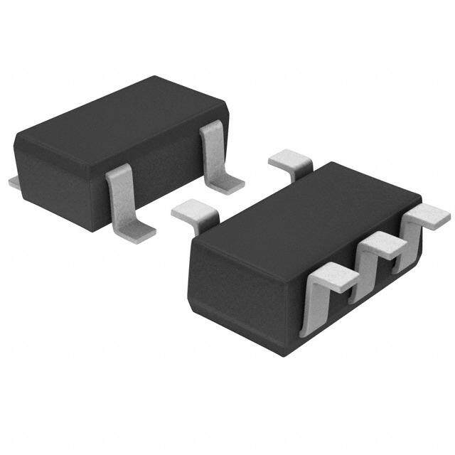
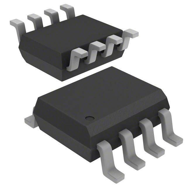
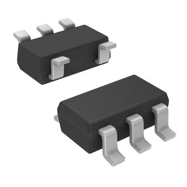
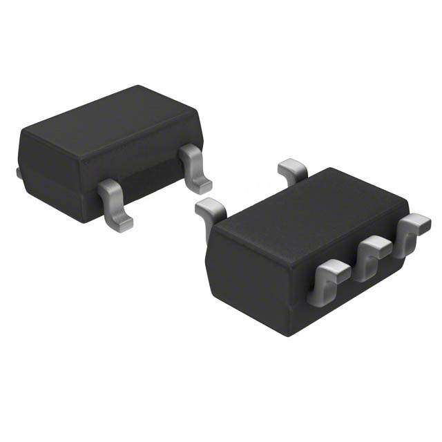
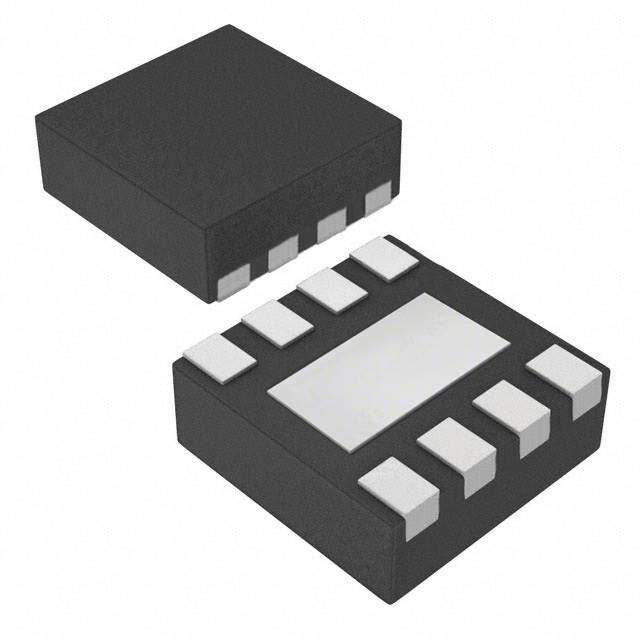
| 产品图片 |
|
| rohs | 符合RoHS无铅 / 符合限制有害物质指令(RoHS)规范要求 |
| 产品系列 | 板上安装温度传感器,Analog Devices AD22105ARZ- |
| 数据手册 | |
| 产品型号 | AD22105ARZ |
| 产品目录页面 | |
| 产品种类 | 板上安装温度传感器 |
| 供应商器件封装 | 8-SOIC |
| 准确性 | 0.5 C |
| 包装 | 管件 |
| 商标 | Analog Devices |
| 安装风格 | SMD/SMT |
| 封装 | Tube |
| 封装/外壳 | 8-SOIC(0.154",3.90mm 宽) |
| 封装/箱体 | SOIC-8 |
| 工厂包装数量 | 98 |
| 感应温度 | -40°C ~ 150°C |
| 数字输出-总线接口 | - |
| 最大工作温度 | + 125 C |
| 最小工作温度 | - 40 C |
| 标准包装 | 98 |
| 电压-电源 | 2.7 V ~ 7 V |
| 电源电压-最大 | 7 V |
| 电源电压-最小 | 2.7 V |
| 电源电流 | 120 uA |
| 精度 | ±0.5°C |
| 系列 | AD22105 |
| 设备功能 | Thermostatic Switch |
| 输出类型 | 开路集电极 |



- 商务部:美国ITC正式对集成电路等产品启动337调查
- 曝三星4nm工艺存在良率问题 高通将骁龙8 Gen1或转产台积电
- 太阳诱电将投资9.5亿元在常州建新厂生产MLCC 预计2023年完工
- 英特尔发布欧洲新工厂建设计划 深化IDM 2.0 战略
- 台积电先进制程称霸业界 有大客户加持明年业绩稳了
- 达到5530亿美元!SIA预计今年全球半导体销售额将创下新高
- 英特尔拟将自动驾驶子公司Mobileye上市 估值或超500亿美元
- 三星加码芯片和SET,合并消费电子和移动部门,撤换高东真等 CEO
- 三星电子宣布重大人事变动 还合并消费电子和移动部门
- 海关总署:前11个月进口集成电路产品价值2.52万亿元 增长14.8%



PDF Datasheet 数据手册内容提取
Low Voltage, Resistor-Programmable, Thermostatic Switch Data Sheet AD22105 FEATURES FUNCTIONAL BLOCK DIAGRAM User-programmable temperature setpoint ±2.0°C maximum ambient setpoint accuracy AD22105 4.1°C typical hysteresis 200kΩ RPULL–UP 1 8 NC Wide supply range: 2.7 V to 7.0 V Wide temperature range: −40°C to +150°C Low power dissipation OUT 2 7 VS SET- APPLICATIONS POINT GND 3 6 RSET Industrial process control TCChoPemUr pmmuaotlne criot tonhrteirnromgl sayl smteamnas gement circuits NC 4 TEMSPEENRSAOTRURE 5 NC 02099-001 Fan control Figure 1. Handheld/portable electronic equipment GENERAL DESCRIPTION The AD22105 is a solid state thermostatic switch. Requiring only one external programming resistor, the AD22105 can be set to switch accurately at any temperature in the −40°C to +150°C wide operating range. Using a novel circuit architecture, the AD22105 asserts an open-collector output when the ambient temperature exceeds the user-programmed setpoint temperature. The AD22105 has approximately 4°C of hysteresis, which prevents rapid thermal on and off cycling. The AD22105 operates on a single power supply voltage from 2.7 V to 7.0 V, facilitating operation in battery-powered applications as well as in industrial control systems. Because of low power dissipation (230 µW at 3.3 V), self heating errors are minimized, and battery life is maximized. An optional internal 200 kΩ pull-up resistor is included to facilitate driving light loads such as complementary metal–oxide semiconductor (CMOS) inputs. Alternatively, a low power light emitting diode (LED) indicator can be driven directly. Rev. A Document Feedback Information furnished by Analog Devices is believed to be accurate and reliable. However, no responsibility is assumed by Analog Devices for its use, nor for any infringements of patents or other One Technology Way, P.O. Box 9106, Norwood, MA 02062-9106, U.S.A. rights of third parties that may result from its use. Specifications subject to change without notice. No license is granted by implication or otherwise under any patent or patent rights of Analog Devices. Tel: 781.329.4700 ©1996–2018 Analog Devices, Inc. All rights reserved. Trademarks and registered trademarks are the property of their respective owners. Technical Support www.analog.com
AD22105 Data Sheet TABLE OF CONTENTS Features .............................................................................................. 1 Effect of Resistor Tolerance and Thermal Drift on Setpoint Applications ....................................................................................... 1 Accuracy .........................................................................................8 General Description ......................................................................... 1 Hysteresis and Self Heating ..........................................................9 Functional Block Diagram .............................................................. 1 Output Section ...............................................................................9 Revision History ............................................................................... 2 Mounting Considerations ............................................................9 Specifications ..................................................................................... 3 Thermal Environment Effects .....................................................9 Absolute Maximum Ratings ............................................................ 4 Using the AD22105 as a Cooling Setpoint Detector ................9 Thermal Resistance ...................................................................... 4 Applications Information .............................................................. 10 ESD Caution .................................................................................. 4 Electromagnetic Interference (EMI) Suppression ................. 10 Pin Configuration and Function Descriptions ............................. 5 Leakage at the RSET Pin ............................................................... 10 Typical Performance Characteristics ............................................. 6 Outline Dimensions ....................................................................... 11 Theory of Operation ........................................................................ 8 Ordering Guide .......................................................................... 11 The Setpoint Resistor ................................................................... 8 REVISION HISTORY 10/2018—Rev. 0 to Rev. A Update Format .................................................................... Universal Changes to Features Section............................................................ 1 Changed Product Description Section to Theory of Operation Section ................................................................................................ 8 Changed Application Hint Section to Applications Information Section .............................................................................................. 10 Updated Outline Dimensions ....................................................... 11 Changes to Ordering Guide .......................................................... 11 1/1996—Revision 0: Initial Version Rev. A | Page 2 of 11
Data Sheet AD22105 SPECIFICATIONS Supply voltage (V) = 3.3 V, T = 25°C, and load resistor (R ) = internal 200 kΩ, unless otherwise noted. S A LOAD Table 1. Parameter Symbol Test Conditions/Comments Min Typ Max Unit TEMPERATURE ACCURACY Ambient Setpoint Accuracy ACC ±0.5 ±2.0 °C Temperature Setpoint Accuracy ACC −40°C ≤ T ≤ +125°C ±3.0 °C T A Power Supply Rejection PSR 2.7 V1 < V < 7.0 V ±0.05 ±0.15 °C/V S HYSTERESIS HYS 4.1 °C OPEN-COLLECTOR OUTPUT Output Low Voltage V Sink current (I ) = 5 mA 250 400 mV OL SINK POWER SUPPLY Supply Voltage Range V 2.7 7.0 V S Supply Current Output Low IS 120 µA ON Output High IS 90 µA OFF INTERNAL PULL-UP RESISTOR R 140 200 260 kΩ PULL-UP TURN-ON SETTLING TIME t 5 µs ON 1 The AD22105 operates at voltages as low as 2.2 V. 39MΩ °C RSET = T S E T ( ° C ) + 2 8 1 . 6 ° C –90.3kΩ 80 75 70 65 60 55 50 kΩ) 45 (ET 40 RS 35 30 25 20 15 10 5 0–50 –25 0SETPO2I5NT TEM5P0ERAT7U5RE (°C1)00 125 150 02099-003 Figure 2. Setpoint Resistor Values Rev. A | Page 3 of 11
AD22105 Data Sheet ABSOLUTE MAXIMUM RATINGS THERMAL RESISTANCE Table 2. Parameter Ratings Thermal performance is directly linked to PCB design and Maximum Supply Voltage 11 V operating environment. Careful attention to PCB thermal Maximum Output Voltage (R ) 11 V design is required. PULL-UP Maximum Output Current (OUT) 10 mA Table 3. Thermal Resistance Operating Temperature Range −40°C to +150°C Package θ (°C/W) τ (sec)1 Dice Junction Temperature 160°C JA SOIC_N (R-8) Storage Temperature Range −65°C to +160°C Moving Air Without Heat Sink2 100 3.5 Lead Temperature (Soldering, 10 sec) 300°C Still Air Without Heat Sink 190 15 Stresses at or above those listed under Absolute Maximum Ratings may cause permanent damage to the product. This is a stress 1 The time constant is defined as the time to reach 63.2% of the final temperature change. rating only; functional operation of the product at these or any 2 1200 cubic feet per minute (CFM) other conditions above those indicated in the operational section of this specification is not implied. Operation beyond the maximum ESD CAUTION operating conditions for extended periods may affect product reliability. Rev. A | Page 4 of 11
Data Sheet AD22105 PIN CONFIGURATION AND FUNCTION DESCRIPTIONS RPULL-UP 1 8 NC OUT 2 AD22105 7 VS GND 3 (NToOt Pto V SIEcaWle) 6 RSET NC 4NC = NO CONNECT5 NC 02099-004 Figure 3. Pin Configuration Table 4. Pin Function Descriptions Pin No. Mnemonic Description 1 R Internal 200 kΩ Pull-Up Resistor (Optional). PULL-UP 2 OUT Device Output. 3 GND Ground. 4, 5, 8 NC No Connect. 6 R Temperature Setpoint Resistor. SET 7 V Supply Voltage. V must be between 2.7 V and 7.0 V. S S Rev. A | Page 5 of 11
AD22105 Data Sheet TYPICAL PERFORMANCE CHARACTERISTICS 4 4.4 3 GUARANTEED LIMIT (+) 4.2 2 C) 4.0 C) 1 S (° OR (° 0 RESI 3.8 R E R T E –1 YS H 3.6 –2 3.4 –3 GUARANTEED LIMIT (–) –4 3.2 –50 –25 0 T2E5MPERA50TURE (7°5C) 100 125 150 02099-005 –50 –25 0 T2E5MPERA50TURE (7°5C) 100 125 150 02099-008 Figure 4. Error vs. Temperature, Setpoint Figure 7. Hysteresis vs. Temperature, Setpoint 2.0 ±0.1 1.5 %) ±0.3 1.0 +125°C C/ C) R (° R (° 0.5 O O NT ERR ±0.5 NT ERR 0 +25°C SETPOI ±0.7 SETPOI –0.5 –40°C –1.0 ±0.9 –1.5 ±1.1–50 –25 0 T2E5MPERA50TURE (7°5C) 100 125 150 02099-006 –2.0 3 4 SUPPLY VO5LTAGE (V) 6 7 02099-009 Figure 5. Setpoint Error vs. Temperature Due to RSET Tolerance Figure 8. Setpoint Error vs. Supply Voltage for Various Temperatures 90 120 VS = 7V 110 80 SUPPLY CURRENT (µA) 7600 VVVSSS === 753VVV SUPPLY CURRENT (µA) 1980000 VS = 5V VS = 3V 50 70 40–50 –25 0 T2E5MPERA50TURE (7°5C) 100 125 150 02099-007 60–50 –25 0 T2E5MPERA50TURE (7°5C) 100 125 150 02099-010 Figure 6. Supply Current (VS) vs. Temperature, Output Voltage (VOUT) = High Figure 9. Supply Current vs. Temperature, VOUT = Low Rev. A | Page 6 of 11
Data Sheet AD22105 0.4 200 W) 0.3 C/ 200 E (° C N V) TA = +125°C TA V (OUT 0.2 TA = +25°C RESIS 150 L A M R 0.1 TA = –40°C HE 100 T 0 50 1µ 10µ IOU1T0 (0Aµ) 1m 10m 02099-011 0 400FLOW RATE (CFM8)00 1200 02099-013 Figure 10. VOUT vs. Output Current (IOUT), VOUT = Low Figure 12. Thermal Resistance (θJA) vs. Flow Rate 16 100 90 14 %) E ( 80 U 12 AL 70 MOVING AIR econds)10 F FINAL V 5600 S(1T2IL0L0c AfmIR) S O ME ( 8 GE 40 TI 6 ENTA 30 C R 20 E 4 P 10 20 400FLOW RATE (CFM8)00 1200 02099-012 00 10 20 TIME (S30econds)40 50 60 02099-014 Figure 11. Time vs. Flow Rate, Thermal Response Figure 13. Percentage of Final Value vs. Time, Thermal Response Time Rev. A | Page 7 of 11
AD22105 Data Sheet THEORY OF OPERATION The AD22105 is a single-supply semiconductor thermostat EFFECT OF RESISTOR TOLERANCE AND THERMAL switch that uses a circuit architecture to realize the combined DRIFT ON SETPOINT ACCURACY functions of a temperature sensor, setpoint comparator, and output Figure 4 shows the typical accuracy error in setpoint stage all in one IC. By using one external resistor, the AD22105 temperature as a function of the programmed setpoint can be programmed to switch at any temperature selected by temperature. This curve assumes an ideal resistor for R . SET the system designer in the −40°C to +150°C range. The internal Figure 5 can be used to calculate additional setpoint error as a comparator is designed to switch accurately as the ambient function of resistor tolerance. Figure 5 shows additional error temperature rises past the setpoint temperature. When the ambient beyond the initial accuracy error of the device and must be temperature falls, the comparator relaxes its output at a somewhat added to the value found in Table 1. For example, consider lower temperature than that at which the comparator originally using the AD22105 programmed to switch at 125°C. Figure 5 switched. The difference between the switch and unswitched indicates that at +125°C, the additional error is approximately temperatures, known as the hysteresis, is nominally 4°C. −0.2°C/% of R . If a 1% resistor (of exactly correct value) is SET THE SETPOINT RESISTOR chosen, the additional error is −0.2°C/% × 1% or −0.2°C. If the closest standard resistor value is 0.6% away from the calculated Determine the setpoint resistor by the following equation: value, the total error is 0.6% for the nominal value and 1% for 39MΩ°C R = − 90.3kΩ (1) the tolerance or 1.006 × 1. 01 or 1.01606 (about 1.6%). The SET TSET(°C) + 281.6°C closest resistor value differing slightly from the calculated value can lead to an additional setpoint error as high as 0.32°C. Connect the setpoint resistor directly between the R pin and SET the GND pin. If a ground plane is used, connect the resistor For additional accuracy considerations, take the thermal drift of directly to this plane at the closest available point. the setpoint resistor into account. For example, consider that the drift of the metal film resistor is 100 ppm/°C. Because this The setpoint resistor, R , can be almost any resistor type. SET drift is usually referred to 25°C, the setpoint resistor can be in However, the resistor initial tolerance and thermal drift affects error by an additional 100 ppm/°C × (125°C − 25°C) or 1%. the accuracy of the programmed switching temperature. For most Using a setpoint temperature of 125°C, this error source adds an applications, a 1% metal film resistor provides the best tradeoff additional −0.2°C (for positive drift) making the overall between cost and accuracy. Calculations for computing an error setpoint error potentially −0.52°C higher than the original budget are found in the Effect of Resistor Tolerance and Thermal accuracy error. Drift on Setpoint Accuracy section. To combine and calculate the initial tolerance and thermal drift After R is calculated, the calculated value does not agree with SET effects of the setpoint resistor use the following equation: readily available standard resistors of the chosen tolerance. To achieve an RSET value as close as possible to the calculated value, RMAX = RNOM × (1 + ε) × (1 + TC × (TSET − 25°C)) a compound resistor can be constructed by connecting two where: resistors in series or in parallel. To conserve cost, one moderately R is the worst case value that the setpoint resistor can be at T . MAX SET precise resistor and one lower precision resistor can be combined. R is the standard resistor with a value closest to the desired R . NOM SET If the moderately precise resistor provides most of the necessary ε is the 25°C tolerance of the chosen resistor (usually 1%, 5%, or resistance, the lower precision resistor can provide a fine 10%). adjustment. Consider an example where the closest standard T is the temperature coefficient of the available resistor. C 1% resistor has only 90% of the value required for R . If a SET T is the desired setpoint temperature. SET 5% series resistor is used for the remainder, the tolerance of After calculation, compare R to the desired R from the resistor only adds 5% of 10% or 0.5% additional error to MAX SET Equation 1. The required value of R at a T of 125°C is the combination. Likewise, the 1% resistor only contributes SET SET 5.566 kΩ. If the nearest standard resistor value is 5.600 kΩ, its worst 90% of 1% or 0.9% error to the combination. These two case maximum value at +125°C is 5.713 kΩ, which is +2.6% contributions are additive, resulting in a total compound higher than R , leading to a total additional error of −0.52°C resistor tolerance of 1.4%. SET beyond that given in Table 1. Rev. A | Page 8 of 11
Data Sheet AD22105 HYSTERESIS AND SELF HEATING THERMAL ENVIRONMENT EFFECTS The actual value of hysteresis generally has a minor dependence on The thermal environment in which the AD22105 is used the programmed setpoint temperature, as shown in Figure 7. determines two performance traits: the effect of self heating on Furthermore, the hysteresis can be affected by self heating if the accuracy and the response time of the sensor to rapid changes in device is driving a heavy load. For example, if the device is driving a temperature. In the first case, a rise in the IC junction temperature load of 5 mA at an output voltage (given by Figure 10) of 250 mV, above the ambient temperature is a function of two variables: the additional power dissipation is approximately 1.25 mW. With a the power consumption of the AD22105 and the thermal θ of 190°C/W in still air, the internal die temperature is 0.24°C resistance between the chip and the ambient environment, θ . JA JA higher than ambient, leading to an increase of 0.24°C in Self heating error can be derived by multiplying the power hysteresis. In the presence of a heat sink or a turbulent dissipation by θ . Because errors of this type can vary widely JA environment, the additional hysteresis is less. for surroundings with different heat sinking capacities, it is OUTPUT SECTION necessary to specify θJA under several conditions. Table 3 shows how the magnitude of self heating error varies The output of the AD22105 is the collector of the negative positive relative to the environment. A typical device dissipates about negative (NPN) transistor. When the ambient temperature of the 230 µW at room temperature with a 3.3 V supply and negligible device exceeds the programmed setpoint temperature, this output loading. In still air, without a heat sink, Table 3 indicates a transistor is activated, causing its collector to become a low θ of 190°C/W, which yields a temperature rise of 0.04°C. impedance. A pull-up resistor, such as the internal 200 kΩ JA Thermal rise of the die is considerably less in an environment of provided, is needed to observe a change in the output voltage. For turbulent or constant moving air or if the device is in direct versatility, the optional pull-up resistor is not permanently physical contact with a solid (or liquid) body. connected to the output pin. Instead, this resistor is undedicated and connects from the V pin to the R pin. To use R , Response of the AD22105 internal die temperature to abrupt S PULL-UP PULL-UP a single connection must be made from the R pin to the changes in ambient temperatures can be modeled by a single time PULL-UP OUT pin. constant exponential function. Figure 12 shows the typical response for moving and still air. The time constant, τ (time to The 200 kΩ pull-up resistor can drive CMOS loads because reach 63.2% of the final value), is dependent on θ and the essentially no static current is required at these inputs. When JA thermal capacities of the chip and the package. driving low power Schottky (LS) and other bipolar family logic inputs, a parallel resistor may be necessary to supply the 20 µA Table 3 lists the effective τ for moving and still air. Copper PCB to 50 µA high level input current (I ) specified for such devices. connections were neglected in the analysis. However, these IH To determine the current required, consult the appropriate connections sink or conduct heat directly through the AD22105 manufacturer data sheet. When the output is switched, indicating solder plated copper leads. When faster response is required, use a an over temperature condition, the output is capable of pulling thermally conductive grease or glue between the AD22105 and down with 10 mA at a voltage of about 375 mV, which allows a the surface temperature being measured. fanout of 2 with standard bipolar logic and 20 with LS family USING THE AD22105 AS A COOLING SETPOINT logic. DETECTOR Low power indicator LEDs (up to 10 mA) can be driven directly The AD22105 detects transitions from higher temperatures to from the output pin of the AD22105. In most cases, a small series lower temperatures by programming the setpoint temperature resistor (usually of several hundred ohms) is required to limit 4°C greater than the desired trip point temperature. The 4°C is the current to the LED and the output transistor of the AD22105. necessary to compensate for the nominal hysteresis value designed MOUNTING CONSIDERATIONS into the device. A more precise value of the hysteresis can be obtained from Figure 7. In this mode, the logic state of the output If the AD22105 is thermally attached and properly protected, it indicates a high for under temperature conditions. The total device can be used in any measuring situation where the maximum error is slightly greater than the specification value due to the range of temperatures encountered is between −40°C and uncertainty in hysteresis. +150°C. Because plastic IC packaging technology is employed, excessive mechanical stress must be avoided when fastening the device with a clamp or screw on the heat tab. Thermally conductive epoxy or glue is recommended for typical mounting conditions. In wet or corrosive environments, use an electrically isolated metal or ceramic well to protect the AD22105. Rev. A | Page 9 of 11
AD22105 Data Sheet APPLICATIONS INFORMATION Figure 14 shows the typical application circuit. LEAKAGE AT THE R PIN SET Leakage currents at the R pin, such as those generated from a SET +2.7V TO +7.0V moist environment or PCB contamination, can have an adverse effect on the programmed setpoint temperature of the AD22105. Depending on the leakage source, leakage current can flow 8 7 6 5 into or out of the RSET pin. Consequently, the actual setpoint temperature may be higher or lower than the intended setpoint temperature by about 1°C for each 75 nA of leakage. With a 5 V AD22105 RSET power supply, an isolation resistance of 100 MΩ creates 50 nA of leakage current, resulting in a setpoint temperature error of about 0.7°C (the R pin is near ground potential). Place a SET 1 2 3 4 guard ring around the RSET node to protect against leakage OUT 02099-002 from the power supply pin (aVsS shown in Figure 15). Figure 14. Typical Application Circuit ELECTROMAGNETIC INTERFERENCE (EMI) SUPPRESSION C1 RSET Noisy environments may couple electromagnetic energy into the R node causing the AD22105 to falsely trip or untrip. SET Noise sources, which typically come from fast rising edges, can be coupled into the device capacitively. Furthermore, if the output signal is close to the R pin, energy can couple from the SET OUT pin to the R pin, potentially causing oscillation. Stray SET capacitance can come from several places such as IC sockets, GND multiconductor cables, and PCB traces. In some cases, cthoinss; tfrourc etxinagm ap Flea, rbayd auys isnhgi eal dsh aireolduendd ctahbel eR wSETit phi nth cea snh cieolrdr ect OUT PIN 1 02099-015 grounded. However, for best performance, avoid cables and Figure 15. Suggested PCB Layout directly solder the AD22105 to a PCB whenever possible. Figure 15 shows a sample PCB layout with low inter pin capacitance and Faraday shielding. If stray capacitance is unavoidable, and interference or oscillation occurs, connect a low impedance capacitor from the R pin to the GND pin. This capacitor SET must be considerably larger than the estimated stray capacitance. Typically, several hundred picofarads corrects the problem. Rev. A | Page 10 of 11
Data Sheet AD22105 OUTLINE DIMENSIONS 5.00(0.1968) 4.80(0.1890) 8 5 4.00(0.1574) 6.20(0.2441) 3.80(0.1497) 1 4 5.80(0.2284) 1.27(0.0500) 0.50(0.0196) BSC 1.75(0.0688) 0.25(0.0099) 45° 0.25(0.0098) 1.35(0.0532) 8° 0.10(0.0040) 0° COPLANARITY 0.51(0.0201) 0.10 SEATING 0.31(0.0122) 0.25(0.0098) 10..2407((00..00510507)) PLANE 0.17(0.0067) COMPLIANTTOJEDECSTANDARDSMS-012-AA (RCINEOFNPEATRRREOENNLCLTEIHNEOGSNDELISYM)AEANNRDSEIAORRNOESUNANORDETEDAIN-POMPFRIFLOLMPIMIRLELIATIMTEEERTFSEO;RIRNECUQHSUEDIVIINMAELDENENSSTIIOGSNNFS.OR 012407-A Figure 16. 8-Lead Standard Small Outline Package [SOIC_N] Narrow Body (R-8) Dimensions shown in millimeters and (inches) ORDERING GUIDE Model1 Temperature Range Package Description Package Option AD22105ARZ −40°C to +150°C 8-Lead Standard Small Outline Package [SOIC_N] R-8 AD22105ARZ-REEL −40°C to +150°C 8-Lead Standard Small Outline Package [SOIC_N] R-8 AD22105ARZ-REEL7 −40°C to +150°C 8-Lead Standard Small Outline Package [SOIC_N] R-8 1 Z = RoHS Compliant Part. ©1996–2018 Analog Devices, Inc. All rights reserved. Trademarks and registered trademarks are the property of their respective owners. D02099-0-10/18(A) Rev. A | Page 11 of 11
Mouser Electronics Authorized Distributor Click to View Pricing, Inventory, Delivery & Lifecycle Information: A nalog Devices Inc.: AD22105AR-REEL AD22105AR-REEL7 AD22105AR AD22105ARZ AD22105ARZ-REEL AD22105ARZ-REEL7
 Datasheet下载


