ICGOO在线商城 > 集成电路(IC) > 线性 - 放大器 - 仪表,运算放大器,缓冲器放大器 > AD202JY
 Datasheet下载
- 型号: AD202JY
- 制造商: Analog
- 库位|库存: xxxx|xxxx
- 要求:
| 数量阶梯 | 香港交货 | 国内含税 |
| +xxxx | $xxxx | ¥xxxx |
查看当月历史价格
查看今年历史价格
AD202JY产品简介:
ICGOO电子元器件商城为您提供AD202JY由Analog设计生产,在icgoo商城现货销售,并且可以通过原厂、代理商等渠道进行代购。 AD202JY价格参考。AnalogAD202JY封装/规格:线性 - 放大器 - 仪表,运算放大器,缓冲器放大器, Isolation Amplifier 2 Circuit 10-SIP。您可以下载AD202JY参考资料、Datasheet数据手册功能说明书,资料中有AD202JY 详细功能的应用电路图电压和使用方法及教程。
| 参数 | 数值 |
| -3db带宽 | - |
| 产品目录 | 集成电路 (IC)半导体 |
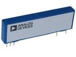
| 描述 | IC OPAMP ISOLATION 2KHZ SIP隔离放大器 IC ISOLATION AMP |
| 产品分类 | Linear - Amplifiers - Instrumentation, OP Amps, Buffer Amps集成电路 - IC |
| 品牌 | Analog Devices |
| 产品手册 | |
| 产品图片 |
|
| rohs | 否不符合限制有害物质指令(RoHS)规范要求 |
| 产品系列 | 放大器 IC,隔离放大器,Analog Devices AD202JY- |
| 数据手册 | |
| 产品型号 | AD202JY |
| PCN设计/规格 | |
| 产品培训模块 | http://www.digikey.cn/PTM/IndividualPTM.page?site=cn&lang=zhs&ptm=30008http://www.digikey.cn/PTM/IndividualPTM.page?site=cn&lang=zhs&ptm=26202 |
| 产品目录页面 | |
| 产品种类 | 隔离放大器 |
| 供应商器件封装 | 10-SIP |
| 共模抑制比—最小值 | 130 dB |
| 包装 | 管件 |
| 压摆率 | - |
| 可用增益调整 | 1 V/V to 100 V/V |
| 商标 | Analog Devices |
| 增益带宽积 | 2kHz |
| 安装类型 | 通孔 |
| 安装风格 | Through Hole |
| 封装 | Tube |
| 封装/外壳 | 38-SIP,10 引线,偏移引线 |
| 封装/箱体 | SIP-10 |
| 工作温度 | 0°C ~ 70°C |
| 工作温度范围 | - 40 C to + 85 C |
| 工作电源电压 | 15 V |
| 工厂包装数量 | 9 |
| 带宽 | 2 kHz |
| 放大器类型 | 隔离 |
| 标准包装 | 1 |
| 电压-电源,单/双 (±) | - |
| 电压-输入失调 | 15mV |
| 电流-电源 | 5mA |
| 电流-输入偏置 | 30pA |
| 电流-输出/通道 | 400µA |
| 电源电流 | 5 mA |
| 电路数 | 2 |
| 系列 | AD202 |
| 绝缘电压 | 750 V |
| 视频文件 | http://www.digikey.cn/classic/video.aspx?PlayerID=1364138032001&width=640&height=505&videoID=2245193153001http://www.digikey.cn/classic/video.aspx?PlayerID=1364138032001&width=640&height=505&videoID=2245193159001 |
| 输入电压范围—最大 | 5 V |
| 输出类型 | - |
| 通道数量 | 4 Channel |


PDF Datasheet 数据手册内容提取
a Low Cost, Miniature Isolation Amplifiers AD202/AD204 FEATURES PRODUCT HIGHLIGHTS Small Size: 4 Channels/lnch The AD202 and AD204 are full-featured isolators offering Low Power: 35 mW (AD204) numerous benefits to the user: High Accuracy: (cid:1)0.025% Max Nonlinearity (K Grade) Small Size: The AD202 and AD204 are available in SIP and High CMR: 130 dB (Gain = 100 V/V) DIP form packages. The SIP package is just 0.25" wide, giving Wide Bandwidth: 5 kHz Full-Power (AD204) the user a channel density of four channels per inch. The isolation High CMV Isolation: (cid:1)2000 V pk Continuous (K Grade) barrier is positioned to maximize input to output spacing. For (Signal and Power) applications requiring a low profile, the DIP package provides a Isolated Power Outputs height of just 0.350". Uncommitted Input Amplifier High Accuracy: With a maximum nonlinearity of ±0.025% APPLICATIONS for the AD202K/AD204K (±0.05% for the AD202J/AD204J) Multichannel Data Acquisition and low drift over temperature, the AD202 and AD204 provide Current Shunt Measurements high isolation without loss of signal integrity. Motor Controls Low Power: Power consumption of 35 mW (AD204) and Process Signal Isolation 75 mW (AD202) over the full signal range makes these isolators High Voltage Instrumentation Amplifier ideal for use in applications with large channel counts or tight GENERAL DESCRIPTION power budgets. The AD202 and AD204 are general purpose, two-port, trans- Wide Bandwidth: The AD204’s full-power bandwidth of 5kHz former-coupled isolation amplifiers that may be used in a broad makes it useful for wideband signals. It is also effective in appli- range of applications where input signals must be measured, cations like control loops, where limited bandwidth could result processed, and/or transmitted without a galvanic connection. in instability. These industry standard isolation amplifiers offer a complete Excellent Common-Mode Performance: The AD202K/ isolation function, with both signal and power isolation provided for in a single compact plastic SIP or DIP style package. The AD204K provide ±2000 V pk continuous common-mode isola- primary distinction between the AD202 and the AD204 is that tion, while the AD202J/AD204J provide ±1000 V pk continuous common-mode isolation. All models have a total common-mode the AD202 is powered directly from a 15 V dc supply while the input capacitance of less than 5 pF inclusive of power isolation. AD204 is powered by an externally supplied clock, such as the This results in CMR ranging from 130 dB at a gain of 100 dB to recommended AD246 Clock Driver. 104 dB (minimum at unity gain) and very low leakage current The AD202 and AD204 provide total galvanic isolation between (2 mA maximum). the input and output stages of the isolation amplifier through the use of internal transformer-coupling. The functionally com- Flexible Input: An uncommitted op amp is provided at the plete AD202 and AD204 eliminate the need for an external, input of all models. This provides buffering and gain as required, user-supplied dc-to-dc converter. This permits the designer and facilitates many alternative input functions including filtering, to minimize the necessary circuit overhead and consequently summing, high voltage ranges, and current (transimpedance) input. reduce the overall design and component costs. Isolated Power: The AD204 can supply isolated power of The design of the AD202 and AD204 emphasizes maximum ±7.5 V at 2 mA. This is sufficient to operate a low-drift input flexibility and ease of use, including the availability of an preamp, provide excitation to a semiconductor strain gage, or uncommitted op amp on the input stage. They feature a bipolar power any of a wide range of user-supplied ancillary circuits. ±5 V output range, an adjustable gain range of from 1V/V to The AD202 can supply ±7.5 V at 0.4 mA, which is sufficient to 100 V/V, ±0.025% max nonlinearity (K grade), 130 dB of operate adjustment networks or low power references and op CMR, and the AD204 consumes a low 35 mW of power. amps, or to provide an open-input alarm. The functional block diagrams can be seen in Figures 1a and 1b. REV.D Information furnished by Analog Devices is believed to be accurate and reliable. However, no responsibility is assumed by Analog Devices for its use, nor for any infringements of patents or other rights of third parties that One Technology Way, P.O. Box 9106, Norwood, MA 02062-9106, U.S.A. may result from its use. No license is granted by implication or otherwise Tel: 781/329-4700 www.analog.com under any patent or patent rights of Analog Devices. Fax: 781/326-8703 © Analog Devices, Inc., 2002
AD202/AD204–SPECIFICATIONS (Typical @ 25(cid:2)C and V = 15 V unless otherwise noted.) S Model AD204J AD204K AD202J AD202K GAIN Range 1 V/V–100 V/V * * * Error ±0.5% typ (±4% max) * * * vs. Temperature ±20 ppm/∞C typ (±45 ppm/∞C max) * * * vs. Time ±50 ppm/1000 Hours * * * vs. Supply Voltage ±0.01%/V ±0.01%/V ±0.01%/V ±0.01%/V Nonlinearity (G = 1 V/V)1 ±0.05% max ±0.025% max ±0.05% max ±0.025% max Nonlinearity vs. Isolated Supply Load ±0.0015%/mA * * * INPUT VOLTAGE RATINGS Input Voltage Range ±5 V * * * Max lsolation Voltage (Input to Output) AC, 60 Hz, Continuous 750 V rms 1500 V rms 750 V rms 1500 V rms Continuous (AC and DC) ±1000 V Peak ±2000 V Peak ±1000 V Peak ±2000 V Peak Isolation-Mode Rejection Ratio (IMRR) @ 60 Hz RS £ 100 W (HI and LO Inputs) G = 1 V/V 110 dB 110 dB 105 dB 105 dB G = 100 V/V 130 dB * * * RS £ l kW (Input HI, LO, or Both) G = 1 V/V 104 dB min 104 dB min 100 dB min 100 dB min G = 100 V/V 110 dB min * * * Leakage Current Input to Output @ 240Vrms,60Hz 2 mA rms max * * * INPUT IMPEDANCE Differential (G = 1 V/V) 1012 W * * * Common-Mode 2 GW(cid:1)4.5 pF * * * INPUT BIAS CURRENT Initial, @ 25∞C ±30 pA * * * vs. Temperature (0∞C to 70∞C) ±10 nA * * * INPUT DIFFERENCE CURRENT Initial, @ 25∞C ±5 pA * * * vs. Temperature (0∞C to 70∞C) ±2 nA * * * INPUT NOISE Voltage, 0.1 Hz to 100 Hz 4 mV p-p * * * f > 200 Hz 50 nV/÷Hz * * * FREQUENCY RESPONSE Bandwidth (VO £ 10 V p-p, G = 1 V–50 V/V) 5 kHz 5 kHz 2 kHz 2 kHz Settling Time, to ±10 mV (10 V Step) 1 ms * * * OFFSET VOLTAGE (RTI) Initial, @ 25∞C Adjustable to Zero (±15 ±15/G)mV max (±5 ± 5/G) mV max (±15 ±15/G) mV max (±5 ±5/G) mV max vs. Temperature (0∞C to 70∞C) ÊÁ±10±1G0ˆ˜mV ∞C * * * Ë ¯ RATED OUTPUT Voltage (Out HI to Out LO) ±5 V * * * Voltage at Out HI or Out LO (Ref. Pin 32) ±6.5 V * * * Output Resistance 3 kW 3 kW 7 kW 7 kW Output Ripple, 100 kHz Bandwidth 10 mV p-p * * * 5 kHz Bandwidth 0.5 mV rms * * * ISOLATED POWER OUTPUT2 Voltage, No Load ±7.5 V * * * Accuracy ±10% * * * Current 2 mA (Either Output)3 2 mA (Either Output)3 400 mA Total 400 mA Total Regulation, No Load to Full Load 5% * * * Ripple 100 mV p-p * * * OSCILLATOR DRIVE INPUT Input Voltage 15 V p-p Nominal 15 V p-p Nominal N/A N/A Input Frequency 25 kHz Nominal 25 kHz Nominal N/A N/A POWER SUPPLY (AD202 Only) Voltage, Rated Performance N/A N/A 15 V ± 5% 15 V ± 5% Voltage, Operating N/A N/A 15 V ± 10% 15 V ± 10% Current, No Load (V = 15 V) N/A N/A 5 mA 5 mA S TEMPERATURE RANGE Rated Performance 0∞C to 70∞C * * * Operating –40∞C to +85∞C * * * Storage –40∞C to +85∞C * * * PACKAGE DIMENSIONS4 SIP Package (Y) 2.08" ¥ 0.250" ¥ 0.625" * * * DlP Package (N) 2.10" ¥ 0.700" ¥ 0.350" * * * NOTES 33 mA with one supply loaded. *Specifications same as AD204J. 4Width is 0.25" typ, 0.26" max. 1Nonlinearity is specified as a % deviation from a best straight line. Specifications subject to change without notice. 21.0mF min decoupling required (see text). –2– REV. D
AD202/AD204 AD246–SPECIFICATIONS PIN DESIGNATIONS (Typical @ 25∞C and VS = 15 V unless otherwise noted.) AD202/AD204 SIP Package Model AD246JY AD246JN Pin Function OUTPUTl 1 +INPUT Frequency 25 kHz Nominal * 2 INPUT/V COMMON ISO Voltage 15 V p-p Nominal * 3 –INPUT Fan-Out 32 Max * 4 INPUT FEEDBACK POWER SUPPLY 5 –V OUTPUT ISO REQUIREMENTS 6 +V OUTPUT Input Voltage 15 V ± 5% * ISO 31 15 V POWER IN (AD202 ONLY) Supply Current Unloaded 35 mA * 32 CLOCK/POWER COMMON Each AD204 Adds 2.2 mA * 33 CLOCK INPUT (AD204 ONLY) Each 1 mA Load on AD204 37 OUTPUT LO +V or –V Adds 0.7 mA * ISO ISO 38 OUTPUT HI NOTES *Specifications the same as the AD246JY. 1The high current drive output will not support a short to ground. AD202/AD204 DIP Package Specifications subject to change without notice. Pin Function AD246 Pin Designations 1 +INPUT Pin (Y) Pin (N) Function 2 INPUT/V COMMON ISO 3 –INPUT 1 12 15 V POWER IN 18 OUTPUT LO 2 1 CLOCK OUTPUT 19 OUTPUT HI 12 14 COMMON 20 15 V POWER IN (AD202 ONLY) 13 24 COMMON 21 CLOCK INPUT (AD204 ONLY) 22 CLOCK/POWER COMMON 36 +V OUTPUT ISO 37 –V OUTPUT ISO 38 INPUT FEEDBACK ORDERING GUIDE Package Max Common-Mode Max Model Option Voltage (Peak) Linearity AD202JY SIP 1000 V ±0.05% AD202KY SIP 2000 V ±0.025% AD202JN DIP 1000 V ±0.05% AD202KN DIP 2000 V ±0.025% AD204JY SIP 1000 V ±0.05% AD204KY SIP 2000 V ±0.025% AD204JN DIP 1000 V ±0.05% AD204KN DIP 2000 V ±0.025% CAUTION ESD (electrostatic discharge) sensitive device. Electrostatic charges as high as 4000 V readily WARNING! accumulate on the human body and test equipment and can discharge without detection. Although the AD202/AD204 features proprietary ESD protection circuitry, permanent damage may occur on devices subjected to high energy electrostatic discharges. Therefore, proper ESD precautions are recommended to avoid performance degradation or loss of functionality. ESD SENSITIVE DEVICE REV. D –3–
AD202/AD204 DIFFERENCES BETWEEN THE AD202 AND AD204 the output leads to get signal inversion. Additionally, in multi- The primary distinction between the AD202 and AD204 is in channel applications, the unbuffered outputs can be multiplexed the method by which they are powered: the AD202 operates with one buffer following the mux. This technique minimizes directly from 15 V dc while the AD204 is powered by a non- offset errors while reducing power consumption and cost. The isolated externally-supplied clock (AD246) that can drive up to output resistance of the isolator is typically 3 kΩ for the AD204 32 AD204s. The main advantages of using the externally- (7 kΩ for AD202) and varies with signal level and temperature, clocked AD204 over the AD202 are reduced cost in multichannel so it should not be loaded (see Figure 2 for the effects of load applications, lower power consumption, and higher bandwidth. upon nonlinearity and gain drift). In many cases, a high imped- In addition, the AD204 can supply substantially more isolated ance load will be present or a following circuit such as an output power than the AD202. filter can serve as a buffer so that a separate buffer function will not often be needed. Of course, in a great many situations, especially where only one or a few isolators are used, the convenience of standalone opera- NON- GAIN GAIN TC tion provided by the AD202 will be more significant than any LINEARITY CHANGE CHANGE (%) (%) (ppm/(cid:3)C) of the AD204’s advantages. There may also be cases where it is 0.25 –10 –500 desirable to accommodate either device interchangeably, so the pinouts of the two products have been designed to make that easy to do. 0.20 –8 –400 FB AD202 0.15 AD202 GAIN AND GAIN TC –6 –300 IN– SIGNAL DEMOD HI AD202 NONLINEARITY VSIG IN+ (cid:1)F5VS MOD F(cid:1)S5V LOVOUT 0.10 AD204 GAIN AND GAIN TC –4 –200 IN COM +VISO OUT +7.5V RECT POWER 0.05 –2 –100 –7.5V AND OSCILLATOR 15V DC –VISO OUT FILTER 25kHz 25kHz AD204 NONLINEARITY POWER 0 0 0 RETURN 0 0.1 0.2 0.3 0.4 0.5 0.6 0.7 0.8 0.9 1.0 OUTPUT LOAD – M(cid:2) Figure 1a.AD202 Functional Block Diagram Figure 2.Effects of Output Loading USING THE AD202 AND AD204 FB AD204 Powering the AD202. The AD202 requires only a single 15 V IN– SIGNAL DEMOD HI power supply connected as shown in Figure 3a. A bypass capaci- IN+ MOD tor is provided in the module. VSIG (cid:1)F5SV F(cid:1)S5V LOVOUT AD202 IN COM –+VVIISSOO OOUUTT +–77..55VV FRAILENTCEDTR 25kHPzOWER25kHz PCOOWNEVR. C1255LVkOH pCz-Kp 15V (cid:1)5% POWER 15V RETURN RETURN Figure 1b.AD204 Functional Block Diagram Figure 3a. (Pin Designations Apply to the DIP-Style Package) Powering the AD204. The AD204 gets its power from an INSIDE THE AD202 AND AD204 externally supplied clock signal (a 15 V p-p square wave with a The AD202 and AD204 use an amplitude modulation technique nominal frequency of 25 kHz) as shown in Figure 3b. to permit transformer coupling of signals down to dc (Figure 1a and 1b). Both models also contain an uncommitted input op AD246 amp and a power transformer that provides isolated power to AD204 AD204 AD204 15V the op amp, the modulator, and any external load. The power transformer primary is driven by a 25 kHz, 15 V p-p square + wave generated internally in the case of the AD202, or supplied externally for the AD204. 15V RETURN Within the signal swing limits of approximately ±5 V, the out- put voltage of the isolator is equal to the output voltage of the Figure 3b. op amp; that is, the isolation barrier has unity gain. The output signal is not internally buffered, so the user is free to interchange (NOTE: Circuit figures shown on this page are for SIP-style packages. Refer to Page 3 for proper DIP package pinout.) –4– REV. D
AD202/AD204 AD246 Clock Driver. The AD246 is a compact, inexpensive AD202 clock driver that can be used to obtain the required clock from a OR single 15 V supply. Alternatively, the circuit shown in Figure 4 100pF RF AD204 (essentially an AD246) can be used. In either case, one clock VO 2k(cid:3) circuit can operate at least 32 AD204s at the rated minimum souppepralyte vdo flotar geea cohf 1440. 2m5V V i nacnrdea osen ein a dsudpitpiolyn vaol litsaoglea tuopr ctoa n1 5b eV. VSIG RG VO = VRSFI G 2(cid:5)0 ( k 1(cid:3) + –RR–GF–) A supply bypass capacitor is included in the AD246, but if many AD204s are operated from a single AD246, an external bypass capacitor should be used with a value of at least 1 mF for every Figure 6.Input Connections for Gain > 1 five isolators used. Place the capacitor as close as possible to the clock driver. The noninverting circuit of Figures 5 and 6 can also be used to your advantage when a signal inversion is needed: just interchange 15V either the input leads or the output leads to get inversion. This 14 6 5 6 approach retains the high input resistance of the noninverting 180pF 1 C TETLSECD4Y2N6E 1N914 circuit, and at unity gain no gain-setting resistors are needed. 3 RC CD Q 10 2 7 COLUKT When the isolator is not powered, a negative input voltage of 49.9k(cid:3)2 R 4047B 4 5 +315(cid:4)VF msigonrael tshoaunr caeb ocuant 2s uVp pwlyil lm caoures et haann i nap fuewt c murAre unnt dtoe rf lsouwc.h Icf otnh-e 1N914 12 9 8 7 4 3 ditions, the 2 kW resistor shown in series with IN+ should be CLK AND used to limit current to a safe value. This is particularly impor- PWR COM tant with the AD202, which may not start if a large input current Figure 4.Clock Driver is present. Input Configurations. The AD202 and AD204 have been Figure 7 shows how to accommodate current inputs or sum designed to be very easy to use in a wide range of applications. currents or voltages. This circuit can also be used when the The basic connection for standard unity gain applications, useful input signal is larger than the ±5 V input range of the isolator; for signals up to ±5 V, is shown in Figure 5; some of the possible for example, a ±50 V input span can be accommodated with variations are described below. When smaller signals must be RF = 20 kW and RS = 200 kW. Once again, a capacitor from FB handled, Figure 6 shows how to achieve gain while preserving a to IN COM is required for gains above five. very high input resistance. The value of feedback resistor R F smhooruel dth bane kfievpet i sa btaokveen 2, 0a k1W0 0f oprF b ceastp arecsituoltrs f.r Womh eFnBe vtoer I Na g CaiOn Mof IS AD202 OR iws irlle qnuoitr aedd.v eArts elloyw aefrf egcati npse rtfhoirsm caanpcaec iitfo ur sise du.nnecessary, but it RS2 RF AD204 V VS2 RS1 FB VS1 IN– OUT 2k(cid:3) HI (SEE TEXT) IN+ ((cid:1)V5SVIG) OUT V(cid:1)O5UVT IN COM LO V = – (VS1 –RR–SF–1 + VS2 –RR–SF–2 + IS RF + ...) 15V OR RF 20k(cid:3) AD202 CLOCK OR Figure 7.Connections for Summing or Current Inputs AD204 Figure 5.Basic Unity-Gain Application (NOTE: Circuit figures shown on this page are for SIP-style packages. Refer to Page 3 for proper DIP package pinout.) REV. D –5–
AD202/AD204 Adjustments. When gain and zero adjustments are needed, the 5k(cid:3) circuit details will depend on whether adjustments are to be made GAIN AD202 OR at the isolator input or output, and (for input adjustments) on RS 47.5k(cid:3) AD204 the input circuit used. Adjustments are usually best done on the input side, because it is better to null the zero ahead of the gain, VS and because gain adjustment is most easily done as part of the 200(cid:3) gain-setting network. Input adjustments are also to be preferred when the pots will be near the input end of the isolator (to mini- 50k(cid:3) +7.5 mize common-mode strays). Adjustments on the output side might be used if pots on the input side would represent a hazard 100k(cid:3) –7.5 ZERO due to the presence of large common-mode voltages during adjustment. Figure 8b.Adjustments for Summing or Current Input Figure 8a shows the input-side adjustment connections for use Figure 9 shows how zero adjustment is done at the output by with the noninverting connection of the input amplifier. The taking advantage of the semi-floating output port. The range of zero adjustment circuit injects a small adjustment voltage in series this adjustment will have to be increased at higher gains; if that with the low side of the signal source. (This will not work if the is done, be sure to use a suitably stable supply voltage for the source has another current path to input common or if current pot circuit. flows in the signal source LO lead). Since the adjustment volt- There is no easy way to adjust gain at the output side of the age is injected ahead of the gain, the values shown will work for isolator itself. If gain adjustment must be done on the output any gain. Keep the resistance in series with input LO below a side, it will have to be in a following circuit such as an output few hundred ohms to avoid CMR degradation. buffer or filter. 5k(cid:3) GAIN AD202 AD202 OR OR 47.5k(cid:3) AD204 AD204 2k(cid:3) VO +15V VS RG 50k(cid:3) 100k(cid:3) ZERO 200(cid:3) 50k(cid:3) +7.5 200(cid:3) 0.1(cid:4)F –15V 100k(cid:3) –7.5 ZERO Figure 9.Output-Side Zero Adjustment Figure 8a. Adjustments for Noninverting Connection of Op Amp Common-Mode Performance. Figures 10a and 10b show how the common-mode rejection of the AD202 and AD204 Also shown in Figure 8a is the preferred means of adjusting the varies with frequency, gain, and source resistance. For these gain-setting network. The circuit shown gives a nominal R of F isolators, the significant resistance will normally be that in the 50 kW, and will work properly for gains of ten or greater. The path from the source of the common-mode signal to IN COM. adjustment becomes less effective at lower gains (its effect is The AD202 and AD204 also perform well in applications re- halved at G = 2) so that the pot will have to be a larger fraction quiring rejection of fast common-mode steps, as described in of the total R at low gain. At G = 1 (follower) the gain cannot F the Applications section. be adjusted downward without compromising input resistance; it is better to adjust gain at the signal source or after the output. 180 Figure 8b shows adjustments for use with inverting input cir- G = 100 G = 1 cuits. The zero adjustment nulls the voltage at the summing 160 node. This method is preferable to current injection because it is RLO = 0(cid:3) less affected by subsequent gain adjustment. Gain adjustment is 140 again done in the feedback; but in this case it will work all the way down to unity gain (and below) without alteration. – dB120 RLO = 500(cid:3) R CM100 RLO = 0(cid:3) 80 RLO = 10k(cid:3) RLO = 10k(cid:3) 60 40 10 20 5060 100 200 500 1k 2k 5k FREQUENCY – Hz Figure 10a.AD204 (NOTE: Circuit figures shown on this page are for SIP-style packages. Refer to Page 3 for proper DIP package pinout.) –6– REV. D
AD202/AD204 180 Except at the highest useful gains, the noise seen at the output G = 100 of the AD202 and AD204 will be almost entirely comprised of G = 1 160 carrier ripple at multiples of 25 kHz. The ripple is typically 2 mV p-p near zero output and increases to about 7 mV p-p for 140 RLO = 0(cid:3) outputs of ±5 V (1 MHz measurement bandwidth). Adding a capacitor across the output will reduce ripple at the expense of – dB120 RLO = 500(cid:3) bandwidth: for example, 0.05 mF at the output of the AD204 CMR 100 RLO = 0(cid:3) wbeil ld roewsunl tt oin 1 1 k.H5 mz.V ripple at ±5 V, but signal bandwidth will RLO = 10k(cid:3) 80 When the full isolator bandwidth is needed, the simple two-pole RLO = 10k(cid:3) active filter shown in Figure 13 can be used. It will reduce ripple 60 to 0.1 mV p-p with no loss of signal bandwidth, and also serves as an output buffer. 40 10 20 5060 100 200 500 1k 2k 5k An output buffer or filter may sometimes show output spikes FREQUENCY – Hz that do not appear at its input. This is usually due to clock noise Figure 10b.AD202 appearing at the op amp’s supply pins (since most op amps have Dynamics and Noise. Frequency response plots for the AD202 little or no supply rejection at high frequencies). Another com- and AD204 are given in Figure 11. Since neither isolator is slew- mon source of carrier-related noise is the sharing of a ground rate limited, the plots apply for both large and small signals. track by both the output circuit and the power input. Figure 13 Capacitive loads of up to 470 pF will not materially affect fre- shows how to avoid these problems: the clock/supply port of the quency response. When large signals beyond a few hundred Hz isolator does not share ground or 15 V tracks with any signal will be present, it is advisable to bypass –V and +V to IN circuits, and the op amp’s supply pins are bypassed to signal ISO ISO COM with 1 mF tantalum capacitors even if the isolated supplies common (note that the grounded filter capacitor goes here as are not loaded. well). Ideally, the output signal LO lead and the supply com- mon meet where the isolator output is actually measured, e.g., At 50 Hz/60 Hz, phase shift through the AD202/AD204 is typically at an A/D converter input. If that point is more than a few feet 0.8∞ (lagging). Typical unit to unit variation is ±0.2∞ (lagging). from the isolator, it may be useful to bypass output LO to sup- 60 ply common at the isolator with a 0.1 mF capacitor. AD204 In applications where more than a few AD204s are driven by a AD202 single clock driver, substantial current spikes will flow in the 40 power return line and in whichever signal out lead returns to a low impedance point (usually output LO). Both of these tracks AMPLITUDE should be made large to minimize inductance and resistance; – dB 20 RESPONSE ideally, output LO should be directly connected to a ground V I plane which serves as measurement common. V/O 0 RESPPOHNASSEE 0 EES Current spikes can be greatly reduced by connecting a small (G = 1) EGR inductance (68 mH–100 mH) in series with the clock pin of each D –20 –50 E AD204. Molded chokes such as the Dale IM-2 series, with dc S HA resistance of about 5 W, are suitable. P –40 –100 10 20 50 100 200 500 1k 2k 5k 10k 20k FREQUENCY – Hz Figure 11.Frequency Response at Several Gains 2200pF AD711 The step response of the AD204 for very fast input signals can 10k(cid:3) 10k(cid:3) be improved by the use of an input filter, as shown in Figure 12. POINT OF The filter limits the bandwidth of the input (to about 5.3 kHz) + + MEASUREMENT 1000pF so that the isolator does not see fast, out-of-band input terms 1.0(cid:4)F 1.0(cid:4)F that can cause small amounts (±0.3%) of internal ringing. The AD204 will then settle to ±0.1% in about 300 ms for a 10 V step. AD202 (IFA DU2S4E6D) OR AD204 AD204 –15V C +15V POWER SUPPLY 3.3k(cid:3) VS 0.01(cid:4)F Figure 13.Output Filter Circuit Showing Proper Grounding Figure 12.Input Filter for Improved Step Response (NOTE: Circuit figures shown on this page are for SIP-style packages. Refer to Page 3 for proper DIP package pinout.) REV. D –7–
AD202/AD204 Using Isolated Power. Both the AD202 and the AD204 provide Operation at Reduced Signal Swing. Although the nominal ±7.5 V power outputs referenced to input common. These may be output signal swing for the AD202 and AD204 is ±5 V, there used to power various accessory circuits that must operate at may be cases where a smaller signal range is desirable. When the input common-mode level; the input zero adjustment pots that is done, the fixed errors (principally offset terms and output described above are an example, and several other possible uses noise) become a larger fraction of the signal, but nonlinearity is are shown in the section titled Application Examples. reduced. This is shown in Figure 15. The isolated power output of the AD202 (400 mA total from 0.025 either or both outputs) is much more limited in current capacity than that of the AD204, but it is sufficient for operating micro- power op amps, low power references (such as the AD589), 0.020 adjustment circuits, and the like. n a p The AD204 gets its power from an external clock driver, and % s can handle loads on its isolated supply outputs of 2 mA for each Y – 0.015 T supply terminal (+7.5 V and –7.5 V) or 3 mA for a single loaded RI A output. Whenever the external load on either supply is more NE0.010 than about 200 mA, a 1 mF tantalum capacitor should be used to NLI O bypass each loaded supply pin to input common. N 0.005 Up to 32 AD204s can be driven from a single AD246 (or equi- valent) clock driver when the isolated power outputs of the AD204s are loaded with less than 200mA each, at a worst-case 0 0 1 2 3 4 5 supply voltage of 14.25 V at the clock driver. The number of OUTPUT SIGNAL SWING – (cid:1)V AD204s that can be driven by one clock driver is reduced by Figure 15.Nonlinearity vs. Signal Swing one AD204 per 3.5 mA of isolated power load current at 7.5 V, distributed in any way over the AD204s being supplied by that PCB Layout for Multichannel Applications. The pinout of clock driver. Thus a load of 1.75 mA from +V to –V would the AD204Y has been designed to make very dense packing ISO ISO also count as one isolator because it spans 15 V. possible in multichannel applications. Figure 16a shows the recommended printed circuit board (PCB) layout for the simple It is possible to increase clock fanout by increasing supply volt- voltage-follower connection. When gain-setting resistors are age above the 14.25 V minimum required for 32 loads. One present, 0.25" channel centers can still be achieved, as shown in additional isolator (or 3.5 mA unit load) can be driven for each Figure 16b. 40 mV of increase in supply voltage up to 15 V. Therefore if the minimum supply voltage can be held to 15 V – 1%, it is possible CHANNEL INPUTS to operate 32 AD204s and 52 mA of 7.5 V loads. Figure 14 shows the allowable combinations of load current and channel 0 1 2 count for various supply voltages. 50 IISO = 0mA TOTAL 40 R OF AD204s DRIVEN 3200 IISIIOS O= =3 57m0mAA T OTOTATALL IISO =T O80TmALA G0R.1ID” E B M CLK COM U N 10 OPERATION IN THIS REGION EXCEEDS CLK 4mA LOAD LIMIT PER AD204 0 OUT COM 14.25 14.50 14.75 15.0 MINIMUM SUPPLY VOLTAGE Figure 14.AD246 Fanout Rules CHANNEL OUTPUTS TO MUX Figure 16a. (NOTE: Circuit figures shown on this page are for SIP-style packages. Refer to Page 3 for proper DIP package pinout.) –8– REV. D
AD202/AD204 CHANNEL 0 CHANNEL 1 Figure 17. A three-pole active filter is included in the design to get normal-mode rejection of frequencies above a few Hz and to HI LO HI LO provide enhanced common-mode rejection at 60 Hz. If offset adjustment is needed, it is best done at the trim pins of the OP07 itself; gain adjustment can be done at the feedback resistor. Note that the isolated supply current is large enough to mandate the use of 1 mF supply bypass capacitors. This circuit can be RF RG RF RG used with an AD202 if a low power op amp is used instead of the OP07. 0.1” GRID Process Current Input with Offset. Figure 18 shows an isolator receiver that translates a 4-20 mA process current 100pF 100pF signal into a 0 V to 10 V output. A 1 V to 5 V signal appears at the isolator’s output, and a –1 V reference applied to output LO provides the necessary level shift (in multichannel applications, 1 1 the reference can be shared by all channels). This technique is 2 2 3 3 often useful for getting offset with a follower-type output buffer. 4 4 5 5 6 6 AD202 OR AD204 +15V + 1V + 4–20mA 250(cid:3) T5OV – 15k(cid:3) 0V –15V TO Figure 16b. 10V –1V TO 1k(cid:3) 10k(cid:3) Synchronization. Since AD204s operate from a common ADDITIONAL – CHANNELS clock, synchronization is inherent. AD202s will normally not 237(cid:3) AD589 interact to produce beat frequencies even when mounted on 0.25-inch centers. Interaction may occur in rare situations where 6.8k(cid:3) a large number of long, unshielded input cables are bundled –15V together and channel gains are high. In such cases, shielded Figure 18. Process Current Input Isolator with Offset cable may be required or AD204s can be used. The circuit as shown requires a source compliance of at least APPLICATIONS EXAMPLES 5 V, but if necessary that can be reduced by using a lower value Low Level Sensor Inputs. In applications where the output of of current-sampling resistor and configuring the input amplifier low level sensors such as thermocouples must be isolated, a low for a small gain. drift input amplifier can be used with an AD204, as shown in 0.15(cid:4)F AD204 39k(cid:3) HI 470k(cid:3) 470k(cid:3) + + 1(cid:4)F AD OP-07 49.9k(cid:3) 0.038(cid:4)F VO = VI (cid:5) ( 1 + 5 0R kG (cid:3) ) – RG LO + 1(cid:4)F 1(cid:4)F CLK 220M(cid:3) + +7.5V OPTIONAL ODPEETNE CINTPIOUNT –7.5V CLK RET Figure 17.Input Amplifier and Filter for Sensor Signals (NOTE: Circuit figures shown on this page are for SIP-style packages. Refer to Page 3 for proper DIP package pinout.) REV. D –9–
AD202/AD204 High Compliance Current Source. In Figure 19, an isolator Floating Current Source/Ohmmeter. When a small floating is used to sense the voltage across current-sensing resistor RS to current is needed with a compliance range of up to ±1000 V dc, allow direct feedback control of a high voltage transistor or FET the AD204 can be used to both create and regulate the current. used as a high compliance current source. Since the isolator has This can save considerable power, since the controlled current virtually no response to dc common-mode voltage, the closed- does not have to return to ground. In Figure 21, an AD589 loop current source has a static output resistance greater than reference is used to force a small fixed voltage across R. That 1014 W even for output currents of several mA. The output sets the current that the input op amp will have to return current capability of the circuit is limited only by power dissipa- through the load to zero its input. Note that the isolator’s out- tion in the source transistor. put isn’t needed at all in this application; the whole job is done by the input section. However, the signal at the output could be –10V TO +250V useful as it’s the voltage across the load, referenced to ground. AD202 Since the load current is known, the output voltage is propor- IL = VRCS LOAD ADO2R04 tional to load resistance. 7.5V AD204 RS 1k(cid:3) 30k(cid:3) LOAD + 470pF 100k(cid:3) 1(cid:4)F + +15V MPS 10k(cid:3) +5V REF AD589 R VO = V R R (cid:5) RL U10 20k(cid:3) – 1k(cid:3) + VC – –15V ILOAD = 1 . 2 R 3 V (2mA MAX) Figure 19. High Compliance Current Source VLOAD 4V Motor Control Isolator. The AD202 and AD204 perform Figure 21.Floating Current Source very well in applications where rejection of fast common-mode Photodiode Amplifier. Figure 22 shows a transresistance steps is important but bandwidth must not be compromised. connection used to isolate and amplify the output of a photo- Current sensing in a fill-wave bridge motor driver (Figure 20) is diode. The photodiode operates at zero bias, and its output one example of this class of application. For 200 V common-mode current is scaled by R to give a 5 V full-scale output. steps (1 ms rise time) and a gain of 50 as shown, the typical F response at the isolator output will be spikes of ±5 mV ampli- tude, decaying to zero in less than 100 ms. Spike height can be AD202 reduced by a factor of four with output filtering just beyond the OR isolator’s bandwidth. 10(cid:4)FAS 500k(cid:3) AD204 PHOTO DIODE 5m(cid:3) (cid:1)20A 0V TO 5V M + + 200V dc – AD204 (cid:1)5V Figure 22.Photodiode Amplifier (cid:1)100mV – Figure 20.Motor Control Current Sensing (NOTE: Circuit figures shown on this page are for SIP-style packages. Refer to Page 3 for proper DIP package pinout.) –10– REV. D
AD202/AD204 OUTLINE DIMENSIONS Dimensions shown in inches and (millimeters) AD202/AD204 SIP Package AD202/AD204 DIP Package 0.250 (6.3) TYP 0.260 (6.6) MAX 2.08 (52.8) MAX 2.100 (53.3) MAX 0.350 (8.9) ADF2R0O2N/TA VIDEW204 (0M1.65A2.9X5) VSIIEDWE (0M2..1I5N0) 0.018 (0.46) 0.015 (0.3M8)AX SQUARE 0.010 (cid:1) 0.020 0.20 (5.1) (0.25 (cid:1) 0.51) 0.15 (3.81) TYP 1 2 3 1819 CL 123456 BOTTOM VIEW 3132 333837 0.1T0Y (P2.5) BOVTIETWOM 0(M1.A770.X80) 383736 222120 0.05 (1.3)TYP 1.30 (33.0) 0.12 0.143 (3.05) 1.60 (40.6) (3.63) NOTE: PIN 31 IS PRESENT ONLY ON AD202 NOTE: PIN 20 IS PRESENT ONLY ON AD202 PIN 33 IS PRESENT ONLY ON AD204 PIN 21 IS PRESENT ONLY ON AD204 C(RINOE FNPETARRREOENLNCLTEIHN EOGSN DELISYM) E AANNRSDEI O ARNROSEU ANNRDOEET D IAN-PO IPNFRFC OHMPEILRSL;IA IMMTIEELT LFEIOMRRE E TUQESUREI VD INAIM LDEEENNSSTIIGSO NFNOSR C(RINOE FNPETARRREOENLNCLTEIHN EOGSN DELISYM) E AANNRSDEI O ARNROSEU ANNRDOEET D IAN-PO IPNFRFC OHMPEILRSL;IA IMMTIEELT LFEIOMRRE E TUQESUREI VD INAIM LDEEENNSSTIIGSO NFNOSR AC1058 Mating Socket AC1060 Mating Socket 0.30 (7.62) 2.60 (66.0) MAX 2.65 (7.30) 2.35 (59.7) 2.50 (63.50) 0.10 (2.50) TYP 0.075 (1.90) TYP 0.24 (6.10) 0.50 0.70 (12.7) (17.8) 0.10 (2.5) DIA AC1058 CAN BE USED AS A SOCKET BOTH ENDS FOR AD202,AD204 AND AD246 0.30 (7.62) MAX NOTE: AMP ZP SOCKET (PIN 2 – 382006 – 3) MAY BE USED IN PLACE OF THE AC1058 0.10 (2.5) DIA 0.125 (3.1) BOTH ENDS TYP CONTROLLING DIMENSIONS ARE IN INCHES; MILLIMETER DIMENSIONS (IN PARENTHESES) ARE ROUNDED-OFF MILLIMETER EQUIVALENTS FOR CONTROLLING DIMENSIONS ARE IN INCHES; MILLIMETER DIMENSIONS REFERENCE ONLY AND ARE NOT APPROPRIATE FOR USE IN DESIGN (IN PARENTHESES) ARE ROUNDED-OFF MILLIMETER EQUIVALENTS FOR REFERENCE ONLY AND ARE NOT APPROPRIATE FOR USE IN DESIGN AD246JY Package AD246JN Package 0.330 (8.4) MAX 1.445 (36.7) MAX 0.995 (25.3) MAX AD246JN 0.35 (8.9) AD246JY 0.625 SIDE FRONT VIEW MAX FRONT VIEW (15.9) VIEW 0.100 (2.5) MAX MIN 0.020 (0.51) 0.020 (0.51) 0.010 (0.25) 0.015 (0.38) 0.015 (0.38) 0.10 0.145 (3.7) 0.010 (0.25) (2.5) 0.05 (1.30) 1.10 (27.9) MIN NOM 0.115 (2.9) 0.10 (2.5) NOM 0.55 (14.0) 1 12 0.197 (5.0) 0.015 (0.38) 0.010 (0.25) 0. 50 0.70 0.115 (12.7) BOTTOM VIEW (17.8) (2.9) 1 13 CL BOVTIETWOM 0(2.1.50) 24 14 2 12 1.00 (25.4) CONTROLLING DIMENSIONS ARE IN INCHES; MILLIMETER DIMENSIONS CONTROLLING DIMENSIONS ARE IN INCHES; MILLIMETER DIMENSIONS (IN PARENTHESES) ARE ROUNDED-OFF MILLIMETER EQUIVALENTS FOR (IN PARENTHESES) ARE ROUNDED-OFF MILLIMETER EQUIVALENTS FOR REFERENCE ONLY AND ARE NOT APPROPRIATE FOR USE IN DESIGN REFERENCE ONLY AND ARE NOT APPROPRIATE FOR USE IN DESIGN REV. D –11–
AD202/AD204 Revision History Location Page 10/02—Data Sheet changed from REV. C to REV. D. Deleted FUNCTIONAL BLOCK DIAGRAM . . . . . . . . . . . . . . . . . . . . . . . . . . . . . . . . . . . . . . . . . . . . . . . . . . . . . . . . . . . . . . . . . 1 Text added to GENERAL DESCRIPTION . . . . . . . . . . . . . . . . . . . . . . . . . . . . . . . . . . . . . . . . . . . . . . . . . . . . . . . . . . . . . . . . . . .1 D) Edits to SPECIFICATIONS TABLE . . . . . . . . . . . . . . . . . . . . . . . . . . . . . . . . . . . . . . . . . . . . . . . . . . . . . . . . . . . . . . . . . . . . . . . .2 2( 0 Edits to Figure 4 . . . . . . . . . . . . . . . . . . . . . . . . . . . . . . . . . . . . . . . . . . . . . . . . . . . . . . . . . . . . . . . . . . . . . . . . . . . . . . . . . . . . . . . .5 10/ – 0 Edits to Input Configurations section . . . . . . . . . . . . . . . . . . . . . . . . . . . . . . . . . . . . . . . . . . . . . . . . . . . . . . . . . . . . . . . . . . . . . . . .5 3– 8 4 Edit to High Compliance Current Source section . . . . . . . . . . . . . . . . . . . . . . . . . . . . . . . . . . . . . . . . . . . . . . . . . . . . . . . . . . . . . . 10 0 0 C Updated OUTLINE DIMENSIONS . . . . . . . . . . . . . . . . . . . . . . . . . . . . . . . . . . . . . . . . . . . . . . . . . . . . . . . . . . . . . . . . . . . . . . . 11 4/01—Data Sheet changed from REV. B to REV. C. Change to SIP Package . . . . . . . . . . . . . . . . . . . . . . . . . . . . . . . . . . . . . . . . . . . . . . . . . . . . . . . . . . . . . . . . . . . . . . . . . . . . . . . . . . 11 A. S. U. N D I E T N RI P –12– REV. D
Mouser Electronics Authorized Distributor Click to View Pricing, Inventory, Delivery & Lifecycle Information: A nalog Devices Inc.: AD202JN AD202JY AD202KN AD202KY AD204JN AD204JY AD204KN AD204KY