ICGOO在线商城 > 隔离器 > 光隔离器 - 逻辑输出 > ACPL-K64L-500E
 Datasheet下载
- 型号: ACPL-K64L-500E
- 制造商: Avago Technologies
- 库位|库存: xxxx|xxxx
- 要求:
| 数量阶梯 | 香港交货 | 国内含税 |
| +xxxx | $xxxx | ¥xxxx |
查看当月历史价格
查看今年历史价格
ACPL-K64L-500E产品简介:
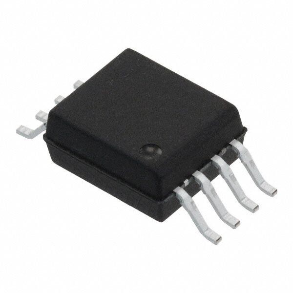
ICGOO电子元器件商城为您提供ACPL-K64L-500E由Avago Technologies设计生产,在icgoo商城现货销售,并且可以通过原厂、代理商等渠道进行代购。 ACPL-K64L-500E价格参考¥20.35-¥20.35。Avago TechnologiesACPL-K64L-500E封装/规格:光隔离器 - 逻辑输出, Logic Output Optoisolator 10MBd 推挽式/图腾柱 5000Vrms 2 Channel 20kV/µs CMTI 8-SO 伸展式。您可以下载ACPL-K64L-500E参考资料、Datasheet数据手册功能说明书,资料中有ACPL-K64L-500E 详细功能的应用电路图电压和使用方法及教程。
| 参数 | 数值 |
| 产品目录 | |
| 描述 | OPTOCOUPLER DGTL 10MBD 8SOIC高速光耦合器 10MBd Optocoupler |
| 产品分类 | |
| 品牌 | Avago Technologies |
| 产品手册 | http://www.avagotech.com/pages/en/optocouplers_plastic/plastic_digital_optocoupler/10_mbd_logic_gate/acpl-k64l-000e/ |
| 产品图片 |
|
| rohs | 符合RoHS无铅 / 符合限制有害物质指令(RoHS)规范要求 |
| 产品系列 | 光耦合器/光电耦合器,高速光耦合器,Avago Technologies ACPL-K64L-500E- |
| 数据手册 | http://www.avagotech.com/docs/AV02-2150EN点击此处下载产品Datasheet |
| 产品型号 | ACPL-K64L-500E |
| PCN封装 | |
| 上升/下降时间(典型值) | 12ns, 12ns |
| 上升时间 | 12 ns |
| 下降时间 | 12 ns |
| 产品种类 | 高速光耦合器 |
| 传播延迟tpLH/tpHL(最大值) | 80ns, 80ns |
| 供应商器件封装 | 8-SO 伸展式 |
| 共模瞬态抗扰度(最小值) | 20kV/µs |
| 其它名称 | 516-3113-6 |
| 包装 | Digi-Reel® |
| 商标 | Avago Technologies |
| 安装类型 | 表面贴装 |
| 封装 | Reel |
| 封装/外壳 | 8-SOIC(0.268",6.81mm 宽) |
| 封装/箱体 | SO-8 |
| 工作温度 | -40°C ~ 105°C |
| 工厂包装数量 | 1000 |
| 数据速率 | 10 MBd |
| 最大功率耗散 | 20 mW |
| 最大反向二极管电压 | 5 V |
| 最大工作温度 | + 105 C |
| 最大正向二极管电压 | 1.7 V |
| 最大正向二极管电流 | 8 mA |
| 最大连续输出电流 | 10 mA |
| 最小工作温度 | - 40 C |
| 最小正向二极管电压 | 0.95 V |
| 标准包装 | 1 |
| 每芯片的通道数量 | 2 Channels |
| 电压-正向(Vf)(典型值) | 1.3V |
| 电压-电源 | 2.7 V ~ 5.5 V |
| 电压-隔离 | 5000Vrms |
| 电流-DC正向(If) | 8mA |
| 电流-输出/通道 | 10mA |
| 绝缘电压 | 3750 Vrms |
| 输入-输入侧1/输入侧2 | 2/0 |
| 输入类型 | DC |
| 输出类型 | 推挽式/图腾柱 |
| 输出设备 | Photo IC |
| 通道数 | 2 |


- 商务部:美国ITC正式对集成电路等产品启动337调查
- 曝三星4nm工艺存在良率问题 高通将骁龙8 Gen1或转产台积电
- 太阳诱电将投资9.5亿元在常州建新厂生产MLCC 预计2023年完工
- 英特尔发布欧洲新工厂建设计划 深化IDM 2.0 战略
- 台积电先进制程称霸业界 有大客户加持明年业绩稳了
- 达到5530亿美元!SIA预计今年全球半导体销售额将创下新高
- 英特尔拟将自动驾驶子公司Mobileye上市 估值或超500亿美元
- 三星加码芯片和SET,合并消费电子和移动部门,撤换高东真等 CEO
- 三星电子宣布重大人事变动 还合并消费电子和移动部门
- 海关总署:前11个月进口集成电路产品价值2.52万亿元 增长14.8%


PDF Datasheet 数据手册内容提取
ACPL-064L, ACPL-M61L, ACPL-W61L, ACPL-K64L Low-Power 10-MBd Digital CMOS Optocouplers Data Sheet Description Features The Broadcom® low-power ACPL-x6xL digital optocouplers Low IDD current: 1.3 mA/channel maximum combine an AlGaAs light emitting diode (LED) and an Low input current: 1.6 mA integrated high gain photodetector. The optocoupler Built-in slew-rate controlled outputs consumes low power, at maximum 1.3 mA I current per DD 20 kV/μs minimum Common-Mode Rejection (CMR) at channel across temperature. With a forward LED current as low V =1000V as 1.6 mA, most microprocessors can directly drive the LED. CM High speed: 10 MBd minimum An internal Faraday shield provides a guaranteed Guaranteed AC and DC performance over wide common-mode transient immunity specification of 20 kV/μs. temperature: –40°C to +105°C Maximum AC and DC circuit isolation is achieved while Wide package selection: SO-5, SO-8, stretched SO-6, and maintaining TTL/CMOS compatibility. stretched SO-8 The optocouplers' CMOS outputs are slew-rate controlled and Safety approval designed to allow the rise and fall time to be controlled over a — UL 1577 recognized: 3750V for 1 minute for rms wide load-capacitance range. ACPL-064L/M61L and 5000V for 1 minute for rms The ACPL-x6xL series operates from both 3.3V and 5V supply ACPL-W61L/K64L voltages with guaranteed AC and DC performance from –40°C — CSA approval to +105°C. — IEC/EN/DIN EN 60747-5-5 approval for Reinforced Insulation These low-power optocouplers are suitable for high speed logic interface applications. RoHS-compliant Functional Diagrams Applications ACPL-M61L ACPL-064L/K64L Communication interfaces: RS485, CANBus, and I2C Microprocessor system interfaces 6 VDD Anode1 1 8 VDD Anode 1 Digital isolation for A/D and D/A converters 5 Vo Cathode1 2 7 Vo1 Cathode3 Cathode2 3 6 Vo2 4 GND Anode2 GND 4 5 SHIELD CAUTION It is advised that normal static precautions be ACPL-W61L taken in handling and assembly of this Anode 1 6 VDD TRUTH TABLE component to prevent damage and/or LED OUTPUT degradation which may be induced by ESD. The NC* 2 5 Vo ON L components featured in this data sheet are not OFF H to be used in military or aerospace applications Cathode 3 4 GND or environments. SHIELD A 0.1 μF bypass capacitor must be connected as close as possible between pins VDD and GND. Broadcom - 1 -
ACPL-064L, ACPL-M61L, ACPL-W61L, ACPL-K64L Data Sheet Ordering Information The ACPL-064L and ACPL-M61L are UL recognized with an isolation voltage of 3750V for 1 minute per UL1577. The ACPL-W61L rms and ACPL-K64L are UL recognized with an isolation voltage of 5000V for 1 minute per UL1577. All devices are RoHS-compliant. rms UL1577 5000 Option IEC/EN/DIN EN Part Number Package Surface Mount Tape and Reel Vrms /1 Minute Quantity RoHS-Compliant 60747-5-5 Rating ACPL-M61L -000E SO-5 X 100 per tube -060E X X 100 per tube -500E X X 1500 per reel -560E X X X 1500 per reel ACPL-064L -000E SO-8 X 100 per tube -060E X X 100 per tube -500E X X 1500 per reel -560E X X X 1500 per reel ACPL-W61L -000E Stretched X X 100 per tube -060E S06 X X X 100 per tube -500E X X X 1000 per reel -560E X X X X 1000 per reel ACPL-K64L -000E Stretched X X 80 per tube -060E S08 X X X 80 per tube -500E X X X 1000 per reel -560E X X X X 1000 per reel To form an ordering part number, choose a part number from the part number column and combine it with the desired option from the RoHS option column. Example: Part number ACPL-M61L-560E describes an optocoupler with a surface mount SO-5 package; delivered in Tape and Reel with 1500 parts-per-reel; with IEC/EN/DIN EN 60747-5-5 Safety Approval; and full RoHS compliance. Option data sheets are available. Contact your Broadcom sales representative or authorized distributor for information. Broadcom - 2 -
ACPL-064L, ACPL-M61L, ACPL-W61L, ACPL-K64L Data Sheet Package Outline Drawings ACPL-064L SO-8 Package Land Pattern Recommendation 1.91 0.64 (0.075) (0.025) 3.937 ±0.127 (0.155 ±0.005) 8 7 6 5 Device Part NNNNV For Option x6xE • Number 3.95 7.49 Lead-Free YYWW Date Code (0.156) (0.295) EEE Lot ID PIN 1 5.994 ±0.203 1 2 3 4 (0.236 ±0.008) 0.406 ±0.076 1.270BSC 1.27 (0.016 ±0.003) (0.050) (0.5) *5.080 ± 0.127 7° 45° X 0.432 (0.200 ± 0.005) (0.017) 3.175 ± 0.127 (0.125 ± 0.005) 0 ~ 7° 0.228 ±0.025 1.524 (0.009 ±0.001) (0.060) * Total package length (inclusive of mold flash) 0.203 ±0.102 5.207 ±0.254 (0.205 ±0.010) 0.305Min.(0.008 ±0.004) Dimensions in Millimeters (Inches). (0.012) Note: Floating lead protrusion is 0.15 mm (6 mils) max. Lead coplanarity = 0.10 mm (0.004 inches) max. Option number 500 not marked. ACPL-M61L SO-5 Package Land Pattern Recommendation 0.33 0.64 DeNvuimceb Pearrt (0.013) 1.27 (0.025) (0.05) For Option x6xE NNNN V • 7.0 ±0.2 4.4 ±0.1 YYWW (0.276 ±0.008) (0.173 ±0.004) 4.39 8.26 EEE Date Code (0.17) (0.325) Lead Free Lot ID Pin 1 Dot 0.4 ±0.05 1.80 (0.016 ±0.002) (0.071) 3.6 ±0.1* 2.54 (0.142 ±0.004) (0.10) 0.102 ±0.102 0.15 ±0.025 2.5 ±0.1 (0.004 ±0.004) (0.098 ±0.004) (0.006 ±0.001) 1.27 BSC 0.71 Min. 7° Max. (0.050) (0.028) Dimensions in millimeters (inches). Max. Lead Coplanarity Note: Foating Lead Protrusion is 0.15 mm (6 mils) max. = 0.102 (0.004) * Maximum Mold flash on each side is 0.15 mm (0.006). Broadcom - 3 -
ACPL-064L, ACPL-M61L, ACPL-W61L, ACPL-K64L Data Sheet ACPL-W61L Stretched SO-6 Package *4.580 ±0.254 (0.180 ±0.010) Land Pattern Recommendation 1.27 (0.050) BSG 12.65 (0.498) 6 5 4 Part Number 0.76 (0.030) RoHS-Compliance For Option x6xE Indicator NNNN V YYWW Date Code EEE Lot ID 1.91 (0.075) 1 2 3 +0.127 6.807 0 (00..308115 ±±00..102075) (0. 268+–00..000050 ) 1.590±0.127 (0.063±0.005) 7° 0.45 (0.018) 7° 45° 3.180±0.127 0.20±0.10 (0.125±0.005) (0.008±0.004) *Total package width (inclusive of mold flash) 0.750±0.250 4.834 ±0.254 mm (0.0295±0.010) Dimensions in millimeters (inches). 11.50±0.250 Lead coplanarity = 0.1 mm (0.004 inches). (0.453±0.010) ACPL-K64L Stretched SO-8 Package *5.850±0.254 (0.230±0.010) Land Pattern Recommendation 8 7 6 5 For Option x6xE Part Number Date Code RoHS-Compliance Indicator NNNN V Lot ID YYWW 6.807±0.127 EEE (0.268±0.005) 1.905 (0.1) 12.650 (0.5) 1 2 3 4 1.590±0.127 (0.063±0.005) 7° 0.450 7° 45° (0.018) 3.180±0.127 0.254±0.100 (0.125±0.005) (0.010±0.004) 0.381±0.13 1.270 (0.050) BSG 0.750±0.250 (0.015±0.005) (0.0295±0.010) * Total package width (inclusive of mold flash) 11.5±0.250 6.100 ±0.254 mm Dimensions in millimeters (inches). (0.453±0.010) Lead coplanarity = 0.1 mm (0.004 inches). Broadcom - 4 -
ACPL-064L, ACPL-M61L, ACPL-W61L, ACPL-K64L Data Sheet Reflow Soldering Profile The recommended reflow soldering conditions are per JEDEC Standard J-STD-020 (latest revision). Non-halide flux should be used. Regulatory Information The ACPL-064L, ACPL-M61L, ACPL-W61L, and ACPL-K64L are approved by the following organizations: IEC/EN/DIN EN 60747-5-5 (Option 060 only) UL — Approval under UL 1577 component recognition program up to VISO = 3750Vrms for the ACPL-M61L/064L and V =5000V for the ACPL-W61L/K64L File E55361. ISO rms CSA — Approval under CSA Component Acceptance Notice #5, File CA 88324. Insulation and Safety Related Specifications ACPL-W61L Parameter Symbol ACPL-064L ACPL-M61L Unit Conditions ACPL-K64L Minimum External Air Gap L(101) 4.9 5 8 mm Measured from input terminals to output (External Clearance) terminals, shortest distance through air. Minimum External Tracking L(102) 4.8 5 8 mm Measured from input terminals to output (External Creepage) terminals, shortest distance path along body. Minimum Internal Plastic Gap 0.08 0.08 0.08 mm Through insulation distance conductor to (Internal Clearance) conductor, usually the straight line distance thickness between the emitter and detector. Tracking Resistance CTI 175 175 175 V VDE 0303-11/DIN EN 60112 (2010-05) (Comparative Tracking Index) Isolation Group IIIa IIIa IIIa Material Group (DIN VDE 0110, 1/89, Table 1) Broadcom - 5 -
ACPL-064L, ACPL-M61L, ACPL-W61L, ACPL-K64L Data Sheet a IEC/EN/DIN EN 60747-5-5 Insulation Characteristics (Option 060) Characteristic Description Symbol Unit ACPL-064L/ ACPL-W61L/ ACPL-M61L ACPL-K64L Installation classification per DIN VDE 0110/39, Table 1 for rated mains voltage ≤ 150V I – IV I – IV rms for rated mains voltage ≤ 300V I – IV I – IV rms I – III I – IV for rated mains voltage ≤ 600V rms I – III for rated mains voltage ≤ 1000V rms Climatic Classification 55/105/21 55/105/21 Pollution Degree (DIN VDE 0110/39) 2 2 Maximum Working Insulation Voltage V 567 1140 V IORM peak Input to Output Test Voltage, Method ba VPR 1063 2137 Vpeak V x 1.875 = V , 100% Production Test with t = 1s, IORM PR m Partial discharge < 5 pC Input to Output Test Voltage, Method aa VPR 907 1824 Vpeak V x 1.6 = V , Type and Sample Test, t = 10s, IORM PR m Partial discharge < 5 pC Highest Allowable Overvoltage (Transient Overvoltage t = 60s) V 6000 8000 V ini IOTM peak Safety-Limiting Values – maximum values allowed in the event of a failure Case Temperature T 150 175 °C S Input Currentb IS, INPUT 150 230 mA Output Powerb PS, OUTPUT 600 600 mW Insulation Resistance at TS, VIO = 500V RS >109 >109 Ω a. Refer to the optocoupler section of the Isolation and Control Components Designer’s Catalog, under Product Safety Regulations section, (IEC/EN/DIN EN 60747-5-5) for a detailed description of Method a and Method b partial discharge test profiles. b. Refer to the following figures for dependence of P and I on ambient temperature: S S Surface Mount SO-8 Product Surface Mount SSO-6/SSO-8 Product 1000 700 PS (mW) PS (mW) POWER OUTPUT – P, INPUT CURRENT – ISS246800000000 IS (mA) POWER OUTPUT – P, INPUT CURRENT – ISS 462135000000000000 IS (mA) 0 0 0 25 50 75 100 125 150 175 0 25 50 75 100 125 150 175 200 TS – CASE TEMPERATURE (°C) TS – CASE TEMPERATURE (°C) NOTE These optocouplers are suitable for safe electrical isolation only within the safety limit data. Maintenance of the safety data shall be ensured by means of protective circuits. Broadcom - 6 -
ACPL-064L, ACPL-M61L, ACPL-W61L, ACPL-K64L Data Sheet Absolute Maximum Ratings Parameter Symbol Min. Max. Unit Condition Storage Temperature T –55 +125 °C S Operating Temperature T –40 +105 °C A Reverse Input Voltage V — 5 V R Supply Voltage V — 6.5 V DD Average Forward Input Current I — 8 mA F Peak Forward Input Current I — 1 A ≤ 1-μs Pulse Width, <300 pulses/second F(TRAN) (IF at 1-μs pulse width, <10% duty cycle) 80 mA ≤ 1-μs Pulse Width, <10% Duty Cycle Output Current I — 10 mA O Output Voltage V –0.5 V + 0.5 V O DD Input Power Dissipation P — 14 mW I Output Power Dissipation P — 20 mW O Lead Solder Temperature T — 260°C for 10s., 1.6 mm below seating plane LS Solder Reflow Temperature Profile See Package Outline Drawings. Recommended Operating Conditions Parameter Symbol Min. Max. Unit Operating Temperature T –40 +105 °C A Input Current, Low Level I 0 250 μA FL Input Current, High Level I 1.6 6.0 mA FH Power Supply Voltage V 2.7 5.5 V DD Forward Input Voltage V — 0.8 V F (OFF) Broadcom - 7 -
ACPL-064L, ACPL-M61L, ACPL-W61L, ACPL-K64L Data Sheet Electrical Specifications (DC) Over the recommended temperature (T = –40°C to +105°C) and supply voltage (2.7V ≤ V ≤ 5.5V). All typical specifications are at A DD V = 5V and T = 25°C. DD A Parameter Symbol Channel Min. Typ. Max. Unit Test Conditions Input Forward Voltage V 0.95 1.3 1.7 V I = 2 mA; Figure1 and Figure2 F F Input Reverse Breakdown Voltage BV 3 5 — V I = 10 μA R R Logic High Output Voltage V V – 0.1 V — V I = 0 mA, V = 0V (R = 1.68 k) OH DD DD F I T or (R = 870), I = –20 μA T O V – 1.0 V — V I = 0 mA, V = 0V (R = 1.68 k) DD DD F I T or (R = 870), I = –3.2 mA T O Logic Low Output Voltage V — 0.03 0.1 V I = 2 mA, V = 5V (R = 1.68 k) OL F I T or V = 3.3V (R = 870), I = 20 μA I T O — 0.18 0.4 V I = 2 mA, V = 5V (R = 1.68 k) F I T or V = 3.3V (R = 870), I = 3.2 mA I T O Input Threshold Current I — 0.7 1.3 mA Figure3 TH Logic Low Output Supply Current I Single — 0.8 1.3 mA Figure4 DDL Dual — 1.6 2.6 Logic High Output Supply Current I Single — 0.8 1.3 mA Figure5 DDH Dual — 1.6 2.6 Input Capacitance C — 60 — pF f = 1 MHz, V = 0V IN F Input Diode Temperature ΔV /ΔT — –1.6 — mV/°C I = 2 mA F A F Coefficient Broadcom - 8 -
ACPL-064L, ACPL-M61L, ACPL-W61L, ACPL-K64L Data Sheet Switching Specifications (AC) Over the recommended temperature (T = –40°C to +105°C) and supply voltage (2.7V ≤ V ≤ 5.5V). All typical specifications are at A DD V = 5V and T = 25°C. DD A Parameter Symbol Min. Typ. Max. Unit Test Conditions Propagation Delay Time to Logic Low Outputa tPHL — 46 80 ns IF = 2 mA, VI = 5V, RT = 1.68 k, C = 15 pF, CMOS Signal Levels. Propagation Delay Time to Logic High Outputa tPLH — 40 80 ns L I = 2 mA, V = 3.3V, R = 870, F I T Pulse Width t 100 — — ns PW C = 15 pF, CMOS Signal Levels. L Pulse Width Distortionb PWD — 6 30 ns Figure6 and Figure7 Propagation Delay Skewc tPSK — 30 ns Output Rise Time (10% to 90%) t — 12 — ns I = 2 mA, V = 5V, R = 1.68 k, R F I T C = 15 pF, CMOS Signal Levels. L — 10 — ns I = 2 mA, V = 3.3V, R = 870, F I T C = 15 pF, CMOS Signal Levels. L Output Fall Time (90% to 10%) t — 12 — ns I = 2 mA, V = 5V, R = 1.68 k, F F I T C = 15 pF, CMOS Signal Levels. L — 10 — ns I = 2 mA, V = 3.3V, R = 870, F I T C = 15 pF, CMOS Signal Levels. L Static Common-Mode Transient Immunity at | CM | 20 35 — kV/μs V = 1000V, T = 25°C, I = 0 mA, H CM A F Logic High Outputd V = 0V (R =1.68 k) or (R = 870), I T T C = 15 pF, CMOS Signal Levels. L Figure8 Static Common-Mode Transient Immunity at | CM | 20 35 — kV/μs V = 1000V, T = 25°C, V = 5 V L CM A I Logic Low Outpute (RT = 1.68 k) or VI = 3.3V (R = 870), I = 2 mA, C = 15 pF, T F L CMOS Signal Levels. Figure8 Dynamic Common-Mode Transient Immunityf CMRD — 35 — kV/μs VCM = 1000 V, TA = 25°C, IF = 2 mA, V = 5V (R = 1.68 k) or V = 3.3 V I T I (R = 870), 10 MBd datarate, T the absolute increase of PWD < 10 ns Figure8 a. t propagation delay is measured from the 50% (V or I ) on the rising edge of the input pulse to the 50% V of the falling edge of the V signal. t PHL in F DD O PLH propagation delay is measured from the 50% (V or I ) on the falling edge of the input pulse to the 50% level of the rising edge of the V signal. in F O b. PWD is defined as |t – t |. PHL PLH c. t is equal to the magnitude of the worst-case difference in t and/or t that is seen between units at any given temperature within the recommended PSK PHL PLH operating conditions. d. CM is the maximum tolerable rate of rise of the common-mode voltage to assure that the output remains in a high logic state. H e. CM is the maximum tolerable rate of fall of the common-mode voltage to assure that the output remains in a low logic state. L f. CM is the maximum tolerable rate of the common-mode voltage during data transmission to assure that the absolute increase of the PWD is less than 10 ns. D Broadcom - 9 -
ACPL-064L, ACPL-M61L, ACPL-W61L, ACPL-K64L Data Sheet Package Characteristics All typicals are at T = 25°C. A Parameter Symbol Part Number Min. Typ. Max. Unit Test Conditions Input-Output Insulation V ACPL-064L 3750 — — V RH < 50% for 1 min. ISO rms ACPL-M61L T = 25°C A ACPL-W61L 5000 — — ACPL-K64L Input-Output Resistance RI-O — 1012 — Ω VI-O = 500V Input-Output Capacitance C — 0.6 — pF f = 1 MHz, T = 25°C I-O A Broadcom - 10 -
ACPL-064L, ACPL-M61L, ACPL-W61L, ACPL-K64L Data Sheet Figure1 Typical Input Diode Forward Current Characteristic Figure2 Typical V versus Temperature F 10 1.50 1.45 A) URRENT (m 1 TA = 25°C OLTAGE (V) 111...334050 WARD C 0.1 IF WARD V 11..2205 I - FORF VF V - FORF11..1105 1.05 0.01 1.00 1.1 1.2 1.3 1.4 1.5 -40 -20 0 20 40 60 80 100 VF - FORWARD VOLTAGE (V) TA - TEMPERATURE (°C) Figure3 Typical Input Threshold Current versus Temperature Figure4 Typical Logic Low Output Supply Current (Per Channel) versus Temperature 1 1 A) m 0.9 NT ( 0.8 PPLY 0.8 E U D CURR 0.6 TPUT SmA) 00..67 SHOL W OUENT ( 0.5 RE 0.4 LORR 0.4 I - INPUT THth 0.2 35.V3V I - LOGIC DDLCU 000...123 35.V3V 0 0 -40 -20 0 20 40 60 80 100 120 -40 0 40 80 120 TA - TEMPERATURE (°C) TA - TEMPERATURE (°C) Figure5 Typical Logic High Output Supply Current (Per Channel) versus Temperature 1 Y 0.9 L P P 0.8 U S T 0.7 TPUmA) 0.6 H OUNT ( 0.5 HIGRRE 0.4 GIC CU 0.3 O - LH 0.2 3.3V DD 0.1 5V I 0 -40 0 40 80 120 TA - TEMPERATURE (°C) Broadcom - 11 -
ACPL-064L, ACPL-M61L, ACPL-W61L, ACPL-K64L Data Sheet Figure6 Typical Switching Speed versus Pulse Input with a 5V Figure7 Typical Switching Speed versus Pulse Input Current with Supply Voltage a 3.3V Supply Voltage 60 60 t - PROPAGATION DELAY;pD-PULSE WIDTH DISTORTION (ns) 12345000000 TTPPPWHLHDL___555...000VVV t - PROPAGATION DELAY;pD-PULSE WIDTH DISTORTION (ns) 12345000000 TTPPPWHLHDL___333...333VVV W W P P -10 -10 1.5 2 2.5 3 3.5 4 4.5 5 5.5 6 1.5 2 2.5 3 3.5 4 4.5 5 5.5 6 IF - PULSE INPUT CURRENT (mA) IF - PULSE INPUT CURRENT (mA) Broadcom - 12 -
ACPL-064L, ACPL-M61L, ACPL-W61L, ACPL-K64L Data Sheet Supply Bypassing, LED Bias Resistors, and PC Board Layout The ACPL-x6xL optocouplers are extremely easy to use and feature high-speed, push-pull CMOS outputs. Pull-up resistors are not required. The external components required for proper operation are the input limiting resistors and the output bypass capacitor. Capacitor values should be 0.1 μF and should be placed as close as possible to the power-supply pins of the optocoupler. For ACPL-M61L/W61L: For ACPL-064L/K64L: V = 3.3V: R = 510 ± 1%, R = 360 ± 1% V = 3.3V: R = 430 ± 1%, R = 430± 1% I 1 2 I 1 2 V = 5.0V: R = 1000 ± 1%, R = 680 ± 1% V = 5.0V: R = 845 ± 1%, R = 845 ± 1% I 1 2 I 1 2 R = R + R R /R = 1.5 R = R + R R /R = 1 T 1 2 1 2 T 1 2 1 2 Figure8 Recommended PCB Layout and Input Current-Limiting Resistor Selection R1 IF R1 IF VI 1 6 VDD VI 1 6 VDD C = 0.1 μF C = 0.1 μF 5 Vo 2 5 Vo R2 R2 GND1 3 4 GND2 GND1 3 4 GND2 ACPL-M61L ACPL-W61L VI R1 IF 1 8 VDD R2 C = 0.1 μF GND1 2 7 Vo1 R2 GND2 3 6 Vo2 R1 IF VI 4 5 GND2 ACPL-064L/K64L 3.3V/5V VDD IF C = 0.1 μF VCM(PEAK) VCM A B Anode Vo 0 V SWITCH AT A: I = 0 mA V VDD F CMH Output O Monitoring V O (min.) SWITCH AT B: I = 2 mA node F Cathode Shield GND V V O (max.) O GND CML VCM Pulse Gen + (cid:16) Broadcom - 13 -
ACPL-064L, ACPL-M61L, ACPL-W61L, ACPL-K64L Data Sheet Propagation Delay, Pulse-Width under the same conditions (i.e., the same supply voltage, Distortion, and Propagation Delay Skew output load, and operating temperature). As shown in Figure10, if the inputs of a group of optocouplers are switched Propagation delay is a figure of merit that describes how either ON or OFF at the same time, t is the difference PSK quickly a logic signal propagates through a system. The between the shortest propagation delay, either t or t , PLH PHL propagation delay from low-to-high (t ) is the amount of and the longest propagation delay, either t or t . As PLH PLH PHL time required for an input signal to propagate to the output, mentioned earlier, t can determine the maximum parallel PSK causing the output to change from low to high. data transmission rate. Similarly, the propagation delay from high-to-low (t ) is the Figure10 is the timing diagram of a typical parallel data PHL amount of time required for the input signal to propagate to application with both the clock and the data lines being sent the output, causing the output to change from high-to-low through optocouplers. The figure shows data and clock signals (see Figure9). at the inputs and outputs of the optocouplers. To obtain the maximum data transmission rate, both edges of the clock Pulse-width distortion (PWD) results when t and t differ PLH PHL signal are being used to clock the data; if only one edge were in value. PWD is defined as the difference between t and PLH used, the clock signal would need to be twice as fast. t . PWD determines the maximum data rate of a transmission PHL system. PWD can be expressed in percent by dividing the PWD Propagation delay skew represents the uncertainty of where an (in ns) by the minimum pulse width (in ns) being transmitted. edge might be after being sent through an optocoupler. Typically, a PWD of 20% to 30% of the minimum pulse width is Figure10 shows that there will be uncertainty in both the data tolerable; the exact figure depends on the particular and the clock lines. It is important that these two areas of application (RS232, RS422, T-1, etc.). uncertainty not overlap. Otherwise the clock signal might Propagation delay skew, t , is an important parameter to arrive before all of the data outputs have settled, or some of the PSK consider in parallel data applications where synchronization of data outputs might start to change before the clock signal has signals on parallel data lines is a concern. arrived. If the parallel data is being sent through a group of From these considerations, the absolute minimum pulse width optocouplers, differences in propagation delays cause the data that can be sent through optocouplers in a parallel application to arrive at the outputs of the optocouplers at different times. If is twice t . A cautious design should use a slightly longer PSK this difference in propagation delays is large enough, it pulse width to ensure that any additional uncertainty in the determines the maximum rate at which parallel data can be rest of the circuit does not cause a problem. sent through the optocouplers. The t specified optocouplers offer the advantages of PSK Propagation delay skew is defined as the difference between guaranteed specifications for propagation delays, pulse-width the minimum and maximum propagation delays, either t or distortion, and propagation delay skew over the PLH t , for any given group of optocouplers which are operating recommended temperature and power supply ranges. PHL Figure9 Propagation Delay Skew Waveform Figure10 Parallel Data Transmission Example VI 50% DATA INPUTS 2.5V, VO CMOS CLOCK tPSK VI 50% DATA OUTPUTS tPSK CLOCK 2.5V, VO CMOS tPSK Broadcom - 14 -
ACPL-064L, ACPL-M61L, ACPL-W61L, ACPL-K64L Data Sheet Optocoupler CMR Performance indicates the typical achievable CMR performance as the input is toggled on or off during a CMR transient. The principal protection against common-mode noise comes The logic output of the ACPL-x6xL optocouplers is mainly from the fundamental isolation properties of the optocoupler, controlled by LED current level, and since the LED current and this in turn is directly related to the Input-Output leakage features very fast rise and fall times, dynamic noise immunity is capacitance of the optocoupler. essentially the same as static noise immunity. To provide maximum protection to circuitry connected to the Despite their immunity to input latch-up and the excellent input or output of the optocoupler, the leakage capacitance is dynamic CMR immunity, ACPL-x6xL optocoupler devices are minimized by having large separation distances at all points in still potentially vulnerable to misoperation caused by turning the optocoupler construction, including the LED/photodiode the LED either on or off during a CMR disturbance. If the LED interface. status could be ensured by design, the overall application level In addition to the optocouplers' basic physical construction, CMR performance would be that of the photodetector. To additional circuit design steps mitigate the effects of benefit from the inherently high CMR capabilities of the common-mode noise. The most important of these is the ACPL-x6xL family, take the following precautions when Faraday shield on the photodetector stage. operating the LED at the application level. A Faraday shield is effective in optocouplers because the In particular, ensure that the LED stays either on or off during a internal modulation frequency (light) is many orders of CMR transient. Some common design techniques to magnitude higher than the common-mode noise frequency. accomplish this include the following: Keep the LED On: Improving CMR Performance at the 1. Overdrive the LED with a higher-than-required forward Application Level current. In an end application, it is desirable that the optocouplers' Keep the LED Off: common-mode isolation be as close as possible to that indicated in the data sheet specifications. The first step in 1. Reverse bias the LED during the off state. meeting this goal is to ensure maximum separation between 2. Minimize the off-state impedance across the anode and PCB interconnects on either side of the optocoupler is cathode of the LED during the off state. maintained and that PCB tracks beneath the optocoupler are All of these methods allow the full CMR capability of the avoided. ACPL-x6xL family to be achieved, but they do have practical It is inevitable that a certain amount of CMR noise will be implementation issues or require a compromise on power coupled into the inputs and this can potentially result in consumption. false-triggering of the input. This problem is frequently There is, however, an effective method to meet the goal of observed in devices with high input impedance. In some cases, maintaining the LED status during a CMR event with no other this can cause momentary missing pulses and can even cause design compromises other than a single added resistor. input circuitry to latch-up in some alternate technologies. This CMR optimization takes advantage of the differential The ACPL-x6xL optocoupler family does not have an input connection to the LED. By ensuring the common-mode latch-up issue. Even at very high CMR levels, such as those impedances at both the cathode and anode of the LED are experienced in end equipment level tests (for example equal, the CMR transient on the LED is effectively canceled. As IEC61000-4-4), the ACPL-x6xL series is immune to latch-up shown in Figure11, this is easily achieved by using two, instead because of the simple diode structure of the LED. of one, input bias resistors. In some cases, achieving the rated data sheet CMR performance level is not possible in an application. This is often because of the practical requirement to actually connect the isolator input to the output of a dynamically changing signal rather than statically tying the input to V or GND. DD To address achievable end application performance on data sheets, the ACPL-x6xL optocouplers include an additional typical performance specification for dynamic CMR in the electrical parameter table. The dynamic CMR specification Broadcom - 15 -
ACPL-064L, ACPL-M61L, ACPL-W61L, ACPL-K64L Data Sheet Split LED Bias Resistor for Optimum CMR For conditions where I is close to the switching threshold (I ), F TH CM also depends on the extent to which I and I balance L LP LN Figure11 shows the recommended drive circuit for the each other. In other words, any condition where a ACPL-x6xL that gives optimum common-mode rejection. The common-mode transient causes a momentary decrease in I F two current-setting resistors balance the common-mode (meaning when dV /dt > 0 and |I | > |I |, referring to CM FP FN impedances at the LED’s anode and cathode. Common-mode Table1) also causes a common-mode failure for transients that transients can capacitively couple from the LED anode (or are fast enough. cathode) to the output-side ground causing current to be Likewise, for a common-mode transient that occurs when the shunted away from the LED (which is not wanted when the LED LED is off (meaning CM , since the output is at high state), if an should be on) or conversely causing current to be injected into H imbalance between I and I results in a transient I equal to the LED (which is not wanted when the LED should be off). LP LN F or greater than the switching threshold of the optocoupler, the Figure12 shows the parasitic capacitances (CLA and CLC) transient signal can cause the output to spike below 2V, which between the LED’s anode and cathode, and output ground. constitutes a CM failure. H Also shown in Figure12 on the input side is an AC-equivalent The resistors recommended in Figure11 include both the circuit. output impedance of the logic driver circuit and the external Table1 shows that the directions of ILP and ILN depend on the limiting resistor. The balanced ILED-setting resistors help polarity of the common-mode transient. For transients equalize the common-mode voltage change at the anode and occurring when the LED is on, common-mode rejection (CML, cathode. This reduces ILED changes caused by transient since the output is at low state) depends on LED current (IF). coupling through the parasitic capacitors CLA and CLC shown in Figure12. For ACPL-M61L/W61L: For ACPL-064L/K64L: V = 3.3V: R = 510 ± 1%, R = 360 ± 1% V = 3.3V: R = 430 ± 1%, R = 430 ± 1% DD 1 2 DD 1 2 V = 5.0V: R = 1000 ± 1%, R = 680 ± 1% V = 5.0V: R = 845 ± 1%, R = 845 ± 1% DD 1 2 DD 1 2 R = R + R R /R = 1.5 R = R + R R /R = 1 T 1 2 1 2 T 1 2 1 2 Figure11 Recommended High-CMR Drive Circuit for the ACPL-x6xL R1 VDD2 VDD VO 0.1(cid:3)μF R2 74LS04 or any totem-pole output logic gate GND2 Shield GND1 Broadcom - 16 -
ACPL-064L, ACPL-M61L, ACPL-W61L, ACPL-K64L Data Sheet For ACPL-M61L/W61L: For ACPL-064L/K64L: V = 3.3V: R = 510 ± 1%, R = 360 ± 1% V = 3.3V: R = 430 ± 1%, R = 430± 1% DD 1 2 DD 1 2 V = 5.0V: R = 1000 ± 1%, R = 680 ± 1% V = 5.0V: R = 845 ± 1%, R = 845± 1% DD 1 2 DD 1 2 R = R + R R /R = 1.5 R = R + R R /R = 1 T 1 2 1 2 T 1 2 1 2 Figure12 AC Equivalent Circuit of ACPL-x6xL R1 VDD2 ILP VO CLA 0.1(cid:3)μF R2 ILN CLC Shield GND2 Table1 Common-Mode Pulse Polarity and LED Current Transient Resultant I Flow Resultant I Flow If |I | < |I |, LED current I If |I | > |I |, LED current I dV /dt Value LP LN LP LN F LP LN F CM Direction Direction is momentarily: is momentarily: Positive (> 0) Away from the LED Away from the LED Increased Decreased anode through C cathode through C LA LC Negative (< 0) Toward the LED Toward the LED Decreased Increased anode through C cathode through C LA LC Broadcom - 17 -
ACPL-064L, ACPL-M61L, ACPL-W61L, ACPL-K64L Data Sheet Slew-Rate Controlled Outputs Feature Figure13 Rise and Fall Time of ACPL-x6xL across Wide-Load Capacitance Typically, the output slew rate (rise and fall time) varies with the output load, as more time is required to charge up the higher Rise Time (VDD = 5.0V) 30 load. The propagation delay and the PWD both increase with the load capacitance. This will be an issue especially in parallel 25 communication because different communication lines will have different load capacitances. However, optocoupler nS) 20 e ( ACPL-x6xL has a built-in slew-rate controlled feature to ensure m 15 Ti that the output slew rate remains stable across wide load e Ris 10 capacitance. Figure13 shows the rise time and fall time for ACPL-x6xL at 3.3V and 5V. 5 10 pF 15 pF 22 pF 33 pF 47 pF 100 pF 0 –40 –20 0 20 40 60 80 100 Temperature (°C) Fall Time (VDD = 5.0V) 25 20 S) n 15 e ( m all Ti 10 F 5 10 pF 15 pF 22 pF 33 pF 47 pF 100 pF 0 –40 –20 0 20 40 60 80 100 Temperature (°C) Rise Time (VDD = 3.3V) 25 20 nS) 15 e ( m Ti 10 e Ris 5 10 pF 15 pF 22 pF 33 pF 47 pF 100 pF 0 –40 –20 0 20 40 60 80 100 Temperature (°C) Fall Time (VDD = 3.3V) 25 20 nS) 15 e ( m e Ti 10 Ris 5 10 pF 15 pF 22 pF 33 pF 47 pF 100 pF 0 –40 –20 0 20 40 60 80 100 Temperature (°C) Broadcom - 18 -
ACPL-064L, ACPL-M61L, ACPL-W61L, ACPL-K64L Data Sheet Speed Improvement Figure15 Improvement of t and PWD with an Added 100-pF p Peaking Capacitor in Parallel of Input Limiting Resistor A peaking capacitor can be placed across the input current-limit resistor (Figure14) to achieve enhanced speed a. V = 5V, C = 47 pF, R = 845 DD peak 1 performance. The value of the peaking capacitor is dependent on the rise and fall time of the input signal, supply voltages, VDD2 = 5V, IF = 2 mA and LED input driving current (I ). Figure15 shows significant 60 F improvement of propagation delay and pulse with distortion 50 TPHL TPLH with an added peak capacitor at a driving current of 2 mA and 3.3V/5V power supply. 40 D (ns) TPHL TPLH W 30 Fthigeu Irnep1u4t L Cimonitniencgt iRoens iosft oPre a(Rk1in) tgo C Iampparcoitvoer S (Cppeeeadk )P ienr Pfoarrmalalenl cweith or PP 20 PWD NWoit Phe Paekainkging t Cpeak 10 0 VDD2 –40 –20 0 20 40 60 80 100 + Temp (°C) R1 V0 Vin 0.1 μF − b. V = 3.3V, C = 47 pF, R = 430 DD peak 1 R2 VDD2 = 3.3V, IF = 2 mA GND1 SHIELD GND2 60 50 TPHL TPLH 40 ns) D ( 30 TPLH No Peaking PW TPHL With Peaking or P 20 t 10 PWD 0 –40 –20 0 20 40 60 80 100 Temp (°C) Broadcom - 19 -
For product information and a complete list of distributors, please go to our web site: www.broadcom.com. Broadcom, the pulse logo, Connecting everything, Avago Technologies, Avago, and the A logo are among the trademarks of Broadcom in the United States, certain other countries and/or the EU. Lead (Pb) Free RoHS 6 fully compliant Copyright © 2016-2018 Broadcom. All Rights Reserved. RoHS 6 fully compliant options available; The term "Broadcom" refers to Broadcom Inc. and/or its subsidiaries. For more -xxxE denotes a lead-free product information, please visit www.broadcom.com. Broadcom reserves the right to make changes without further notice to any products or data herein to improve reliability, function, or design. Information furnished by Broadcom is believed to be accurate and reliable. However, Broadcom does not assume any liability arising out of the application or use of this information, nor the application or use of any product or circuit described herein, neither does it convey any license under its patent rights nor the rights of others. AV02-2150EN – June 6, 2018
Mouser Electronics Authorized Distributor Click to View Pricing, Inventory, Delivery & Lifecycle Information: B roadcom Limited: ACPL-064L-000E ACPL-M61L-000E ACPL-M61L-060E ACPL-M61L-500E ACPL-M61L-560E ACPL-064L-060E ACPL-064L-500E ACPL-064L-560E ACPL-K64L-000E ACPL-K64L-060E ACPL-K64L-500E ACPL-K64L-560E ACPL-W61L-000E ACPL-W61L-060E ACPL-W61L-500E ACPL-W61L-560E