ICGOO在线商城 > 光电元件 > 光纤 - 收发器模块 > ABCU-5740RZ
- 型号: ABCU-5740RZ
- 制造商: Avago Technologies
- 库位|库存: xxxx|xxxx
- 要求:
| 数量阶梯 | 香港交货 | 国内含税 |
| +xxxx | $xxxx | ¥xxxx |
查看当月历史价格
查看今年历史价格
ABCU-5740RZ产品简介:
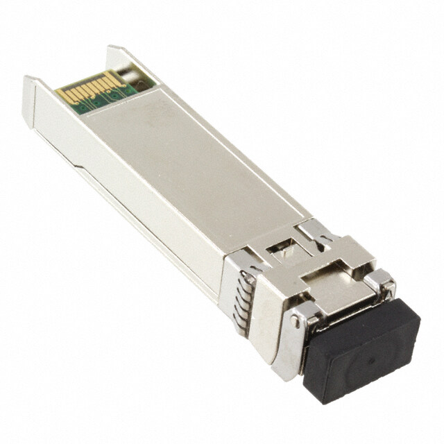
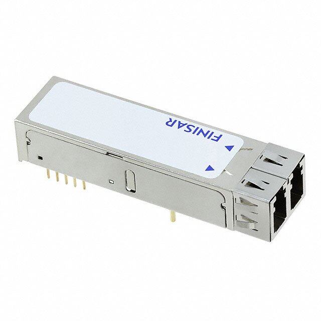
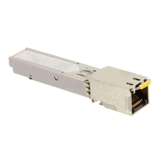
ICGOO电子元器件商城为您提供ABCU-5740RZ由Avago Technologies设计生产,在icgoo商城现货销售,并且可以通过原厂、代理商等渠道进行代购。 ABCU-5740RZ价格参考。Avago TechnologiesABCU-5740RZ封装/规格:光纤 - 收发器模块, Fiber Optic Transceiver Module 以太网 1.25Gbd 3.3V RJ45 可插入式,SFP。您可以下载ABCU-5740RZ参考资料、Datasheet数据手册功能说明书,资料中有ABCU-5740RZ 详细功能的应用电路图电压和使用方法及教程。
| 参数 | 数值 |
| 产品目录 | |
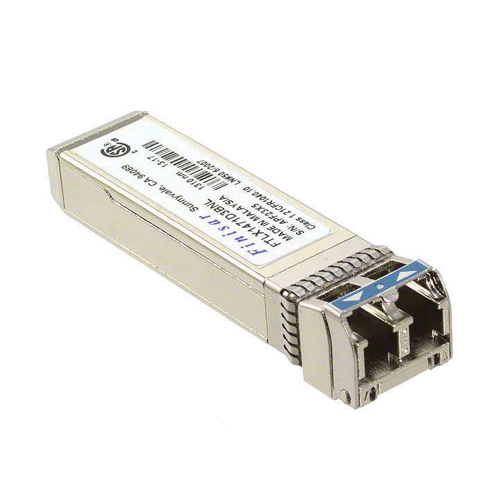
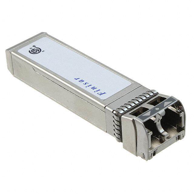
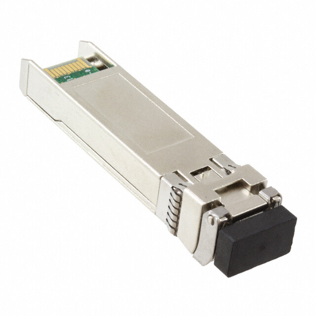
| 描述 | TXRX RJ-45 SFP 1.25GBD光纤发射器、接收器、收发器 SGMII |
| 产品分类 | 光纤 - 收发器光纤 |
| 品牌 | Avago Technologies US Inc. |
| 产品手册 | http://www.avagotech.com/docs/AV02-3410EN |
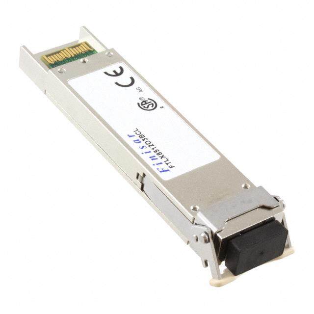
| 产品图片 |
|
| rohs | 符合RoHS无铅 / 符合限制有害物质指令(RoHS)规范要求 |
| 产品系列 | 光纤发射器、接收器、收发器,Avago Technologies ABCU-5740RZ- |
| mouser_ship_limit | 该产品可能需要其他文件才能进口到中国。 |
| 数据手册 | http://www.avagotech.com/docs/AV02-3410EN |
| 产品型号 | ABCU-5740RZ |
| 产品 | Transceivers |
| 产品种类 | 光纤发射器、接收器、收发器 |
| 其它名称 | 516-2879 |
| 商标 | Avago Technologies |
| 外观尺寸或封装类型 | SFP |
| 安装类型 | * |
| 安装风格 | Panel |
| 封装 | Bulk |
| 封装/箱体 | SFP-20 |
| 工作电源电压 | 3.3 V |
| 工厂包装数量 | 10 |
| 应用 | 以太网 |
| 数据速率 | 1.25Gbd |
| 最大工作温度 | + 85 C |
| 最大输出电流 | 5 mA |
| 最小工作温度 | - 40 C |
| 标准包装 | 10 |
| 波长 | - |
| 特色产品 | http://www.digikey.cn/product-highlights/cn/zh/avago-altera-optical-networking-solutions/3959 |
| 电压-电源 | 3.3V |
| 连接器类型 | RJ45 |




- 商务部:美国ITC正式对集成电路等产品启动337调查
- 曝三星4nm工艺存在良率问题 高通将骁龙8 Gen1或转产台积电
- 太阳诱电将投资9.5亿元在常州建新厂生产MLCC 预计2023年完工
- 英特尔发布欧洲新工厂建设计划 深化IDM 2.0 战略
- 台积电先进制程称霸业界 有大客户加持明年业绩稳了
- 达到5530亿美元!SIA预计今年全球半导体销售额将创下新高
- 英特尔拟将自动驾驶子公司Mobileye上市 估值或超500亿美元
- 三星加码芯片和SET,合并消费电子和移动部门,撤换高东真等 CEO
- 三星电子宣布重大人事变动 还合并消费电子和移动部门
- 海关总署:前11个月进口集成电路产品价值2.52万亿元 增长14.8%



PDF Datasheet 数据手册内容提取
ABCU-57xxxxZ Family 10/100/1000BASE-T 1.25 GBd Small Form Pluggable Low Voltage (3.3 V) Electrical Transceiver over Category 5 Cable Data Sheet Description Features The ABCU-57xxxxZ family of electrical transceivers from RoHS-6 Compliant (see Table 1) Avago Technologies off er full-duplex throughput of 1000 Designed for Industry-Standard, Small Form Factor Mbps by transporting data over shielded and unshielded Pluggable (SFP) Ports twisted pair category 5 cable with 5-level PAM (Pulse Compliance with IEEE 802.3:2005 Amplitude Modulation) signals. Custom RJ-45 connector with integrated magnetics The Avago Technologies 1000BASE-T module takes sig- Link lengths at 1.25 Gbd: up to 100 m per IEEE802.3 nals from both the twisted pair category 5 cable and the SerDes interface. Pin count overhead between the MAC Low power, high performance 1.25 Gbd SerDes inte- grated in module and the PHY is minimized, and Gigabit Ethernet opera- tion is achieved with maximum space savings. Single +3.3 V power supply operation Auto-negotiation per IEEE 802.3:2005 Clause 28 Product Ordering Information (Twisted Pair) and Clause 37 (1000BASE-X) ABCU-5730RZ -5~70 RX_LOS enabled Compatible to both shielded and unshielded twisted pair category 5 cable ABCU-5740RZ -5~70 RX_LOS disabled ABCU-5730GZ -5~70 RX_LOS enabled & Isolated Available in Commercial Temperature (-5~70 °C) and ground Industrial Temperature (-40~85 °C) ABCU-5730ARZ -40~85 RX_LOS enabled 10/100/1000BASE-T operation available with SGMII host systems. ABCU-5740ARZ -40~85 RX_LOS disabled ABCU- 5740AGZ -40~85 RX_LOS disabled Applications & Isolated ground Switch to switch interface ABCU-5731ARZ -40~85 SGMII RX_LOS enabled Switched backplane applications ABCU-5741ARZ -40~85 SGMII RX_LOS disabled File server interface ABCU-5741AGZ -40~85 SGMII RX_LOS disabled & Isolated ground Module Diagrams ABCU-5731RZ -5~70 SGMII RX_LOS enabled Figure 1 illustrates the major functional components ABCU-5741RZ -5~70 SGMII RX_LOS disabled of the ABCU-57xxxxZ family of transceivers. The 20-pin connection diagram of module printed circuit board of Related Products the module is shown in Figure 2. Figure 3 depicts the pin assignment of the MDI (RJ45 jack). AFBR-5710Z Family of 850nm +3.3V SFP optical Figure 6 depicts the external confi guration and dimen- transceivers for Gigabit Ethernet sions of the module. AFCT-5710Z Family of 1310nm +3.3V SFP optical transceivers for Gigabit Ethernet
Installation Serial Identifi cation (EEPROM) The ABCU-57xxxxZ family can be installed in or removed The ABCU-57xxxxZ family complies with an industry stan- from any MultiSource Agreement (MSA) compliant Small dard MultiSource Agreement that defi nes the serial identi- Form Pluggable port whether the host equipment is fi cation protocol. This protocol uses the 2-wire serial CMOS operating or not. The module is simply inserted, small EEPROM protocol of the ATMEL AT24C01A or equivalent. end fi rst, under fi nger-pressure. Controlled hot-plugging The contents of the ABCU-57xxxxZ family serial ID memory is ensured by design and by 3-stage pin sequencing at are defi ned in Table 10 as specifi ed in the SFP MSA. the electrical interface to the host board. The module Controller and Data I/O housing makes initial contact with the host board EMI shield, mitigating potential damage due to ElectroStatic Data I/Os are designed to accept industry standard dif- Discharge (ESD). The module pins sequentially contact ferential signals. In order to reduce the number of passive the (1) Ground, (2) Power, and (3) Signal pins of the host components required on the customer’s board, Avago board surface mount connector. This printed circuit board Technologies has included the functionality of the trans- card-edge connector is depicted in Figure 2. mitter bias resistors and coupling capacitors within the module. The transceiver is compatible with an “ac-coupled” TX_DISABLE confi guration and is internally terminated. Figure 1 depicts TX_DATA the functional diagram of the ABCU-57xxxxZ family of RX_DATA transceivers. 100-ohm resistor shown at RX_LOS in Figure 1 refers to ABCU-573xxxZ confi guration. RX_LOS 100 SerDes/ Magnetics RJ45 DSP Adapter Caution should be taken into account for the proper inter- MOD_DEF2 connection between the supporting Physical Layer integrat- MOD_DEF1 ed circuits and the ABCU-57xxxxZ family of transceivers. MOD_DEF0 100 Figure 4 illustrates the recommended interface circuit. Several control data signals and timing diagrams are imple- mented in the module and are depicted in Figure 6. EEPROM Figure 1. Transceiver Functional Diagram PIN 1 PIN 8 20 V T 1 V T EE EE 19 TD- 2 TX_FAULT 18 TD+ 3 TX_DISABLE 17 V T 4 MOD-DEF(2) EE 16 V T 5 MOD-DEF(1) CC 15 V R 6 MOD-DEF(0) CC 14 V R 7 Rate Select EE 13 RD+ 8 LOS 12 RD- 9 V R EE 11 V R 10 V R EE EE Figure 3. MDI ( RJ 45 Jack) Pin Assignment Bottom of Board Top of Board (as viewed thru top of board) Note: LOS is only applicable for ABCU-573xxxZ models Figure 2. 20-pin Connection Diagram of Module Printed Circuit Board 2
V_SUPPLY VCC_T ABCU-57xxxxZ 1 uH 10 uF 0.1 uF 0.1 uF VCC_R 1 uH 10 uF 0.1 uF 4.7 K TX_DISABLE TX_FAULT PHY 100 IC TD+ TX[0:9] 0.01 uF 100 TD- SerDes 0.01 uF RJ45 JACK & CAT5 PROTOCOL IC RD+ MAGNETICS CABLE RX[0:9] 100 0.01 uF 100 RD- 0.01 uF RX_LOS *100 MOD_DEF 1 MOD_DEF 2 MOD_DEF 0 EEPROM 100 REF CLK 4.7 K 4.7 K 4.7 K 4.7 K * All models that have LOS disabled, will ground the LOS pin through a 100 ohm internal resistor. V_SUPPLY Figure 4. Typical Application Confi guration for ABCU-57xxxxZ 1 μH V T CC 0.1 μF 1 μH V R 3.3 V CC 0.1 μF 10 μF 0.1 μF 10 μF SFP MODULE HOST BOARD Note: Inductors must have less than 1ohm series resistance per MSA Figure 5. MSA Recommended Power Supply Filter 3
Application Support Electrostatic Discharge (ESD) Evaluation Kit There are two conditions in which immunity to ESD dam- age is important. Table 1 documents our immunity to To help you in your preliminary transceiver evaluation, both of these conditions. The fi rst condition is during han- Avago Technologies off ers a 1.25 GBd Gigabit Ethernet dling of the transceiver prior to insertion into the trans- evaluation board. This board will allow testing of the ceiver port. To protect the transceiver, it is important to electrical parameters of transceiver. Please contact your use normal ESD handling precautions. These precautions local Field Sales representative for availability and order- include using grounded wrist straps, work benches, and ing details. fl oor mats in ESD controlled areas. The ESD sensitivity of the ABCU-57xxxxZ is compatible with typical industry Regulatory Compliance production environments. See Table 1 for transceiver Regulatory Compliance perfor- The second condition is static discharges to the exterior mance. The overall equipment design will determine the of the host equipment chassis after installation. To the certifi cation level. The transceiver performance is off ered extent that the RJ45 connector interface is exposed to the as a fi gure of merit to assist the designer. outside of the host equipment chassis, it may be subject to system-level ESD requirements. The ESD performance Immunity of the ABCU-57xxxxZ exceeds typical industry standards. Equipment hosting the ABCU-57xxxxZ modules will be subjected to radio-frequency electromagnetic fi elds in some environments. The transceivers have excellent im- munity to such fi elds due to their shielded design. Table 1. Regulatory Compliance Feature Test Method Performance Electrostatic Discharge MIL-STD-883C Method 3015.4 Class 2 (2000 Volts) (ESD) to the Electrical JEDEC/EIA JES022-A114-A Pins Electrostatic Discharge Variation of IEC 61000-4-2 Typically withstand 15 KV ( Air Discharge), 8 KV (ESD) to the RJ 45 (Contact) without damage when the RJ 45 connector Connector Receptacle receptacle is contacted by a Human Body Model probe. Electromagnetic FCC Part 15 Class B System margins are dependent on customer board and Interference (EMI) CENELEC EN55022 Class B chassis design. (CISPR 22A)VCCI Class 1 Radiated Immunity Variation of IEC 61000-4-3 Typically shows a negligible eff ect from a 10 V/m fi eld swept from 80 to 1000 MHz applied to the transceiver without a chassis enclosure. Component Underwriters Laboratories and Canadian UL File # E173874 Recognition Standards Association Joint Component Recognition for Information Technology Equipment Including Electrical Business Equipment Grounding DC short between signal and chassis - Meets all regulatory requirements as listed above. Confi guration grounds - Compliant with system boards using multi-point grounding scheme ROHS Compliance Chemical composition analysis Less than 0.1% lead, mercury, hexavalent chromium, polybrominated biphenyls, and polybrominated biphenyl ethers by weight of homogeneous material. Exemption for lead in high melting temperature solder applied to module connector. Less than 0.01% cadmium by weight of homogeneous material. 4
Electromagnetic Interference (EMI) Caution Most equipment designs utilizing these high-speed trans- There are no user serviceable parts nor any maintenance ceivers from Avago Technologies will be required to meet required for the ABCU-57xxxxZ. Tampering with or the requirements of FCC in the United States, CENELEC modifying the performance will result in voided product EN55022 (CISPR 22A) in Europe and VCCI in Japan. warranty. It may also result in improper operation of the ABCU-57xxxxZ circuitry, and possible overstress of the The metal housing and shielded design minimize the RJ 45 connector. Device degradation or product failure EMI challenge facing the host equipment designer. These may result. Connecting the module to a non-approved transceivers provide superior EMI performance. This 1000BaseT module, operating above the recommended greatly assists the designer in the management of the absolute maximum conditions or operating the ABCU- overall system EMI performance. 57xxxxZ in a manner inconsistent with its design and Flammability function may result in hazardous radiation exposure and may be considered an act of modifying or manufacturing The ABCU-57xxxxZ electrical transceiver housing is an electrical module product. made of metal and high strength, heat resistant, chemi- cally resistant, and UL 94V-0 fl ame retardant plastic. Ordering Information Please contact your local fi eld sales engineer or one of Avago Technologies franchised distributors for ordering information. For technical information, please visit Avago Technologies web page at www.avagotech.com or con- tact Avago Technologies Customer Response Center. For information related to the MSA visit www.schelto.com/ SFP/index.html Customer Manufacturing Processes This module is pluggable and is not designed for aqueous wash, IR refl ow or wave soldering processes. 5
Table 2. 20-pin Connection Diagram Description Pin Name Function/Description MSA Notes 1 VEET Transmitter Ground 2 TX Fault Transmitter Fault Indication - High Indicates a Fault Note 1 3 TX Disable Transmitter Disable - Module disables on high or open Note 2 4 MOD-DEF2 Module Defi nition 2 - Two wire serial ID interface Note 3 5 MOD-DEF1 Module Defi nition 1 - Two wire serial ID interface Note 3 6 MOD-DEF0 Module Defi nition 0 - Grounded in module Note 3 7 Rate Select Not Connected 8 LOS Loss of Signal - High Indicates Loss of Signal Note 4 9 VEER Receiver Ground 10 VEER Receiver Ground 11 VEER Receiver Ground 12 RD- Inverse Received Data Out Note 5 13 RD+ Received Data Out Note 5 14 VEER Receiver Ground 15 VCCR Receiver Power - 3.3 V +/- 5% Note 6 16 VCCT Transmitter Power - 3.3 V +/- 5% Note 6 17 VEET Transmitter Ground 18 TD+ Transmitter Data In Note 7 19 TD- Inverse Transmitter Data In Note 7 20 VEET Transmitter Ground Notes: 1. TX Fault is not used and is always tied to ground through a 100 ohm resistor. 2. TX Disable as described in the MSA is not applicable to the 1000BASE-T module, but is used for convenience as an input to reset the internal ASIC. This pin is pulled up within the module with a 4.7 K resistor. Low (0 – 0.8 V): Transceiver on Between (0.8 V and 2.0 V): Undefi ned High (2.0 – 3.465 V): Transceiver in reset state Open: Transceiver in reset state 3. Mod-Def 0,1,2. These are the module defi nition pins. They should be pulled up with a 4.7-10 K resistor on the host board to a supply less than VCCT + 0.3 V or VCCR + 0.3 V. Mod Def 0 is tied to ground through a 100 ohm resistor to indicate that the module is present. Mod-Def 1 is clock line of two wire serial interface for optional serial ID Mod-Def 2 is data line of two wire serial interface for optional serial ID 4. LOS (Loss of Signal) operation on the 1000BaseT SFP is diff erent than for optical SFP applications. For models with RX_LOS enabled, RX_LOS signal is a 1000BASE-T linkup/link-down indicator and not a peak (AC) or voltage (DC) detector. For models where RX_LOS is disabled, RX_LOS is not used and is always tied to ground via 100-ohm resistor. 5. RD-/+: These are the diff erential receiver outputs. They are ac coupled 100 diff erential lines which should be terminated with 100 diff erential at the user SerDes. The ac coupling is done inside the module and is thus not required on the host board. The voltage swing on these lines will be between 370 and 2000 mV diff erential (185 – 1000 mV single ended) when properly terminated. These levels are compatible with CML and LVPECL voltage swings. 6. VCCR and VCCT are the receiver and transmitter power supplies. They are defi ned as 3.3 V ± 5% at the SFP connector pin. The maximum supply current is 317 mA and the associated in-rush current will typically be no more than 30 mA above steady state after 500 nanoseconds. 7. TD-/+: These are the diff erential transmitter inputs. They are ac coupled diff erential lines with 100 diff erential termination inside the module. The ac coupling is done inside the module and is thus not required on the host board. The inputs will accept diff erential swings of 500 – 2400 mV (250 – 1200 mV single ended), though it is recommended that values between 500 and 1200 mV diff erential (250 – 600 mV single ended) be used for best EMI performance. These levels are compatible with CML and LVPECL voltage swings. 6
Absolute Maximum Ratings Parameter Symbol Minimum Typical Maximum Unit Notes Storage Temperature TS -40 +85 °C Note 1 Case Temperature TC -40 +85 °C Note 1 ,2 Relative Humidity RH 5 95 % Note 1 Module Supply Voltage VCCT,R -0.5 3.6 V Note 1, 2 Data/Control Input Voltage VI -0.5 VCC V Note 1 Sense Output Current - MOD-DEF2 5.0 mA Recommended Operating Conditions Parameter Symbol Minimum Typical Maximum Unit Notes Case Temperature TC -5 70 °C Note 3 -40 85 °C Module Supply Voltage VCCT,R 3.135 3.3 3.465 V Note 3 Data Rate 1.25 Gb/s Note 3 Transceiver Electrical Characteristics (T = -5 °C to +70 °C, V T,R = 3.3 V ± 5%) (Tc = -40 °C to +85°C, VccT,R = 3.3 V +/- 5%) C CC Parameter Symbol Minimum Typical Maximum Unit Notes AC Electrical Characteristics Power Supply Noise Rejection PSNR 100 mV Note 4 (peak-peak) DC Electrical Characteristics Module supply current (TC = -5 °C to +70 °C, VCCT,R = 3.3 V ± 5%) ICC 350 mA (Tc = -40 °C to +85°C, VccT,R = 3.3 V +/- 5%) 370 Power Dissipation (TC = -5 °C to +70 °C, VCCT,R = 3.3 V ± 5%) PDISS 1100 mW (Tc = -40 °C to +85°C, VccT,R = 3.3 V +/- 5%) 1150 Sense Outputs: VOH 2.0 VCCT, R+ 0.3 V Note 5 MOD-DEF2 RX_LOS VOL 0 0.4 Control Inputs: VIH 2.0 VCC V Note 5 Transmitter Disable(TX_DISABLE), MOD-DEF1, 2 VIL 0 0.8 V Notes: 1. Absolute Maximum Ratings are those values beyond which damage to the device may occur if these limits are exceeded for other than a short period of time. See Reliability Data Sheet for specifi c reliability performance. 2. Between Absolute Maximum Ratings and the Recommended Operating Conditions functional performance is not intended, device reliability is not implied, and damage to the device may occur over an extended period of time. 3. Operating conditions will vary, depending on model. Recommended Operating Conditions are those values outside of which functional perfor- mance is not intended, device reliability is not implied, and damage to the device may occur over an extended period of time. See Reliability Data Sheet for specifi c reliability performance later when it is ready. 4. MSA-specifi ed fi lter is required on the host board to achieve PSNR performance over the frequency range 10 Hz to 2 MHz. 5. LVTTL, external 4.7-10 K pull-Up resistor required for MOD-DEF 1 and MOD-DEF 2. 7
Transmitter and Receiver Electrical Characteristics (T = -5 °C to +70 °C, V T,R = 3.3 V ± 5%) (Tc = -40 °C to +85°C, VccT,R = 3.3 V +/- 5%) C CC Parameter Symbol Minimum Typical Maximum Unit Notes Data Input: Transmitter Diff erential VI 330 2400 mV Note 1 Input Voltage (TD +/-) Data Output: Receiver Diff erential VO 370 735 2000 mV Note 2 Output Voltage (RD +/-) Receive Data Rise & Fall Times Trf 100 250 ps Note 3 (Receiver) Transceiver Timing Characteristics (T = -5 °C to +70 °C, V T,R = 3.3 V ± 5%) (Tc = -40 °C to +85°C, VccT,R = 3.3 V +/- 5%) C CC Parameter Symbol Minimum Typical Maximum Unit Notes Tx Disable Assert Time t_off NA Note 4 Tx Disable Negate Time t_on NA Note 4 Module Reset Assert Time t_off _rst 10 s Note 5 Module Reset Negate Time t_on_rst 300 ms Note 6 Time to initialize t_init 300 ms Tx Fault Assert Time t_fault NA Note 7 Tx Disable to Reset t_reset NA Note 7 LOS Assert Time t_loss_on NA Note 7 LOS De-assert Time t_loss_off NA Note 7 Rate Select Change Time t_ratesel NA Note 7 Serial ID Clock Rate F_serial_clock 100 kHz Notes: 1. Internally ac coupled and terminated (100 Ohm diff erential). These levels are compatible with CML and LVPECL voltage swings. 2. Internally ac coupled with an external 100 ohm diff erential load termination. 3. 20%-80% rise and fall times measured with a 500 MHz signal utilizing a 1010 pattern. 4. Tx Disable function as described in the SFP MSA is not used in the 1000BASE-T module. 5. Time from rising edge of Tx Disable until link comes down. 6. Time from falling edge of Tx Disable until auto-negotiation starts. 7. Not used in the 1000BASE-T module 8
VCC > 3.15 V POWER SAVING (TX_DISABLE) TRANSMITTED SIGNAL (AUTO-NEGOTIATION BEGINS) t_init t-init: MODULE HOT-PLUGGED OR VOLTAGE APPLIED AFTER INSERTION, WHEN TX_DISABLE IS NEGATED VCC > 3.15 V TX_DISABLE t_on_rst TRANSMITTED SIGNAL (AUTO-NEGOTIATION BEGINS) t_init t-init: VOLTAGE APPLIED WHEN TX_DISABLE IS ASSERTED Tx_DISABLE TRANSMITTED SIGNAL (AUTO-NEGOTIATION BEGINS ON RISING EDGE) t_off_rst t_on_rst t_off_rst & t_on_rst: TX_DISABLE (RESET) ASSERTED THEN DE-ASSERTED Figure 6. Transceiver Timing Diagrams (Module Installed Except Where Noted) 9
Table 3. EEPROM Serial ID Memory Contents at address A0 Addr Hex ASCII Addr Hex ASCII Addr Hex ASCII Addr Hex ASCII 0 03 40 41 A 68 Note 3 96 Note 5 1 04 41 42 B 69 Note 3 97 Note 5 2 00 42 43 C 70 Note 3 98 Note 5 3 00 43 55 U 71 Note 3 99 Note 5 4 00 44 2D - 72 Note 3 100 Note 5 5 00 45 35 5 73 Note 3 101 Note 5 6 08 46 37 7 74 Note 3 102 Note 5 7 00 47 Note 1 75 Note 3 103 Note 5 8 00 48 Note 1 76 Note 3 104 Note 5 9 00 49 Note 1 77 Note 3 105 Note 5 10 00 50 Note 1 78 Note 3 106 Note 5 11 01 51 Note 1 79 Note 3 107 Note 5 12 0D 52 20 80 Note 3 108 Note 5 13 00 53 20 81 Note 3 109 Note 5 14 00 54 20 82 Note 3 110 Note 5 15 00 55 20 83 Note 3 111 Note 5 16 00 56 20 84 Note 4 112 Note 5 17 00 57 20 85 Note 4 113 Note 5 18 64 58 20 86 Note 4 114 Note 5 19 00 59 20 87 Note 4 115 Note 5 20 41 A 60 00 88 Note 4 116 Note 5 21 56 V 61 00 89 Note 4 117 Note 5 22 41 A 62 00 90 Note 4 118 Note 5 23 47 G 63 Note 2 91 Note 4 119 Note 5 24 4F O 64 00 92 00 120 Note 5 25 20 65 Note 1 93 00 121 Note 5 26 20 66 00 94 00 122 Note 5 27 20 67 00 95 Note 2 123 Note 5 28 20 124 Note 5 29 20 125 Note 5 30 20 126 Note 5 31 20 127 Note 5 32 20 33 20 34 20 35 20 36 01 37 00 38 17 39 6A Notes: 1. The contents of these registers will change dependent on model number. 2. Addresses 63 and 95 are check sums. Address 63 is the check sum for bytes 0-62 and address 95 is the check sum for bytes 64-94. 3. Address 68-83 specify a unique identifi er. 4. Address 84-91 specify the date code. 5. These fi elds are reserved for optional use by Avago Technologies. 10
Internal ASIC Registers The registers are accessible through the 2-wire se- rial CMOS EEPROM protocol of the ATMEL AT24C01A The ASIC (or “PHY”, for Physical Layer IC) in the trans- or equivalent. The address of the PHY is 1010110x, ceiver module contains 32 registers. Each register where x is the R/W bit. Each register’s address is contains 16 bits. The registers are summarized in 000yyyyy, where yyyyy is the binary equivalent of the table 11 and detailed in table 12 through 28. Each bit register number. Write and read operations must send is either Read Only (RO) or Read/Write (R/W). Some or receive 16 bits of data, so the “multi-page” access bits are also described as Latch High (LH) or Latch protocol must be used. Low (LL) and/or Self Clearing (SC). Table 4. Summary of Internal IC Registers Register Description 0 Control 1 Status 2-3 N/A for SFP Module 4 Auto-Negotiation Advertisement 5 Auto-Negotiation Link Partner Ability 6 Auto-Negotiation Expansion 7 Auto-Negotiation Next Page Transmit 8 Auto-Negotiation Link Partner Received Next Page 9 MASTER-SLAVE Control Register 10 MASTER-SLAVE Status Register 11-15 N/A for SFP Module 16 Extended Control 1 17 Extended Status 1 18-19 N/A for SFP Module 20 Extended Control 2 21 Receive Error Counter 22 Cable Diagnostic 1 23-25 N/A for SFP Module 26 Extended Control 3 27 Extended Status 2 28 Cable Diagnostic 2 29-31 N/A for SFP Module 11
Table 5. Register 0 (Control) Hardware Software Bit Name Description Reset Reset Details 0.15R/W Reset 1 = PHY reset 0 self-clearing Performs software reset 0 = Normal Operation 0.14R/W Loopback 1 = Enable 0 0 Serial data in on RD+/- is deserial- 0 = Disable ized, then reserialized and sent out on TD+/- 0.13R/W Speed Selection 0 = 1000 Mb/s 0 Update Paired with bit 0.6. Module may (LSB) function at speeds other than 1000 MB/s depending on model This bit is only meaningful if bit 0.12 is 0. 0.12R/W Auto-Negotiation 1 = Enable 1 Update Changes to this bit take eff ect Enable 0 = Disable after software reset. 0.11R/W Power Down 1 = Power Down 0 0 0 = Normal Operation 0.10R/W Isolate 1 = Isolate 0 0 0 = Normal Operation 0.9R/W/SC Restart Auto- 1 = Restart Auto-Nego- 0 Self-clearing Negotiation tiation Process 0 = normal operation 0.8R/W Duplex Mode 1 = Full Duplex 1 Update This bit is only meaningful if 0.12 0 = Half Duplex is 0. 0.7R/W Collision Test 1 = enable COL signal 0 0 test 0 = disable COL signal test 0.6R/W Speed Selection 1 = 1000 Mb/s 1 Update Paired with bit 0.13. Module may (MSB) function at speeds other than 1000 MB/s depending on model This bit is only meaningful if bit 0.12 is 0. 0.5:0R/W N/A to SFP Module 000000 000000 12
Table 6. Register 1 (Status) Hardware Software Bit Name Description Reset Reset Details 1.15:9 N/A to SFP Module 0000000 0000000 RO 1.8 Extended Status 1 = Extended status information in register 15 1 1 Always 1 RO 1.7 N/A to SFP Module 0 0 RO 1.6 MF Preamble 1 = PHY will accept management frames with 1 1 Always 1 RO Suppression preamble suppressed. 1.5 Auto-Negotiation 1 = Auto-Negotiation Process Completed 0 0 RO Complete 0 = Auto-Negotiation Process Not Completed 1.4 Remote Fault 1 = remote fault condition detected 0 0 RO/LH 0 - no remote fault condition detected 1.3 Auto-Negotiation 1 = module is able to perform Auto-Negoti- 1 1 RO Ability ation 0 = module is unable to perform Auto-Nego- tiation 1.2 Link Status 1 = link is up 0 0 RO/LL 0 = link is down 1.1 Jabber Detect 1 = jabber condition detected 0 0 RO/LH 0 = no jabber condition detected 1.0 Extended Capability 1 = extended register capabilities 1 1 Always 1 RO 13
Table 7. Register 4 (Auto-Negotiation Advertisement) Hardware Software Bit Name Description Reset Reset Details 4.15:14 N/A to SFP Module 10 10 When writing to register 4, be R/W sure to preserve the values of these bits. Changes to these values can interrupt the normal operation of the SFP module. 4.13 Remote Fault 1 = Remote fault bit is set 0 Retain This bit takes eff ect after auto- R/W 0 = No remote fault negotiation is restarted, either via bit 0.9 or because the link goes down. 4.12 N/A to SFP Module 0 Retain R/W 4.11:10 PAUSE Encoding 11 = Both Asymmetric 00 Retain This bit takes eff ect after auto- R/W PAUSE and Symmetric negotiation is restarted, either PAUSE toward local device via bit 0.9 or because the link 10 = Asymmetric PAUSE goes down. toward link partner 01 = Symmetric PAUSE 00 = No PAUSE 4.9 N/A to SFP Module 0 0 R/W 4.8 100BASE-TX Full 1 = Advertise PHY is 1 (for ABCU- Retain This bit takes eff ect auto-negoti- R/W Duplex 100BASE-TX full duplex 57x1-XXX) ation is restarted via bit 0.9 capable 0 (for ABCU- 0 = Advertise PHY is not 57x0-XXX) 100BASE-TX full duplex capable 4.7 100BASE-TX Half 1 = Advertise PHY is 1 (for ABCU- Retain This bit takes eff ect auto-negoti- R/W Duplex 100BASE-TX half duplex 57x1-XXX) ation is restarted via bit 0.9 capable 0 (for ABCU- 0 = Advertise PHY is not 57x0-XXX) 100BASE-TX half duplex capable 4.6 10BASE-T Full- 1 = Advertise PHY is 1 (for ABCU- Retain This bit takes eff ect auto-negoti- R/W Duplex 10BASE-T full duplex 57x1-XXX) ation is restarted via bit 0.9 capable 0 (for ABCU- 0 = Advertise PHY is not 57x0-XXX) 10BASE-T full duplex capable 4.5 10BASE-T Half- 1 = Advertise PHY is 1 (for ABCU- Retain This bit takes eff ect auto-negoti- R/W Duplex 10BASE-T half duplex 57x1-XXX) ation is restarted via bit 0.9 capable 0 (for ABCU- 0 = Advertise PHY is not 57x0-XXX) 10BASE-T half duplex capable 4.4:0 IEEE 802.3 Selector 00001 00001 Set per IEEE standard. RO Field 14
Table 8. Register 5 (Auto-Negotiation Link Partner Ability) Hardware Software Bit Name Description Reset Reset Details 5.15 Next Page 1 = Link partner advertises next page 0 0 RO ability 0 = Link partner does not advertise next page ability 5.14 Acknowledge 1 = Link partner acknowledges receiv- 0 0 RO ing link code word from module 0 = Link partner does not acknowledge receiving link code word from module 5.13 Remote Fault 1 = Link partner has a remote fault 0 0 RO 0 = Link partner does not have a remote fault 5.12 N/A to SFP Module 0 0 RO 5.11:10 PAUSE Encoding 11 = Asymmetric PAUSE and Symmetric 00 00 RO PAUSE toward local device 10 = Asymmetric PAUSE toward link partner 01 = Symmetric PAUSE 00 = No PAUSE 5.9:5 N/A to SFP Module 00000 00000 RO 5.4:0 IEEE 802.3 Selector Field 00000 00000 Set per RO IEEE standard. Table 9. Register 6 (Auto-Negotiation Expansion) Hardware Software Bit Name Description Reset Reset Details 6.15:5 N/A to SFP Module 00000000000 00000000000 RO 6.4 Parallel Detection 1 = A fault has been detected via 0 0 This register is not RO Fault the Parallel Detection function valid until auto- 0 = A fault has not been detected negotiation is com- via the Parallel Detection function plete, as indicated by bit 1.5. 6.3 Link Partner Next 1 = Link partner is next page able 0 0 See note in bit 6.4. RO Page Able 0 = Link partner is not next page able 6.2 Next Page Able 1 = Local device is next page able 1 1 See note in bit 6.4. RO 0 = Local device is not next page able 6.1 Page Received 1 = A new page has been received 0 0 See note in bit 6.4. RO/LH 0 = A new page has not been received 6.0 Link Partner Auto- 1 = Link partner is auto-negotia- 0 0 See note in bit 6.4. RO Negotiation Able tion able 0 = Link partner is not auto-nego- tiation able 15
Table 10. Register 7 (Auto-Negotiation Next Page Transmit Register) Hardware Software Bit Name Description Reset Reset Details 7.15 Next Page 1 = Additional next pages 0 0 R/W to follow 0 = Last page 7.14 N/A to SFP Module 0 0 RO 7.13 Message Page 1 = Message page 1 1 R/W 0 = Unformatted page 7.12 Acknowledge 2 1 = Will comply with 0 0 R/W message 0 = Will not comply with message 7.11 Toggle 1 = previous value of the 0 0 RO toggle bit was0 0 = previous value of the toggle bit was 1 7.10:0 Message/Unformatted 00000000001 00000000001 R/W Code Field Table 11. Register 8 (Auto-Negotiation Link Partner Received Next Page) Hardware Software Bit Name Description Reset Reset Details 8.15 Next Page 1 = Additional next pages 0 0 RO to follow 0 = Last page 8.14 Acknowledge 0 0 RO 8.13 Message Page 1 = Message page 0 0 RO 0 = Unformatted page 8.12 Acknowledge 2 1 = Will comply with mes- 0 0 RO sage 0 = Will not comply with message 8.11 Toggle 1 = previous value of the 0 0 RO toggle bit was 0 0 = previous value of the toggle bit was 1 8.10:0 Message/Unformatted 00000000000 00000000000 RO Code Field 16
Table 12. Register 9 (MASTER-SLAVE Control) Software Bit Name Description Hardware Reset Reset Details 9.15:13 Transmitter Test 000 = Normal Operation 000 000 The module enters test modes R/W Mode 001 = Transmit Waveform Test when MDI crossover is fi rst 010 = Transmit Jitter Test in disabled via bits 16.6:5. MASTER Mode 011 = Transmit Jitter Test in SLAVE Mode 9.12 MASTER-SLAVE 1 = Enable MASTER-SLAVE 0 Retain This bit takes eff ect after auto- R/W Manual Confi g Manual confi guration value in negotiation is restarted via Enable register 9.11 bit 0.9. 0 = Disable MASTER-SLAVE Manual confi guration value in register 9.11 9.11 MASTER-SLAVE 1 = Confi gure PHY as MAS- 1 Retain This bit takes eff ect after auto- R/W Confi g Value TER during MASTER-SLAVE negotiation is restarted via bit negotiation 0.9. This bit is ignored unless 0 = Confi gure PHY as SLAVE bit 9.12 is 1. during MASTER-SLAVE nego- tiation 9.10 Port Type 1 = Prefer PHY as MASTER 1 Retain This bit takes eff ect after auto- R/W (multiport) negotiation is restarted via bit 0 = Prefer PHY as SLAVE (single 0.9. This bit is ignored unless port) bit 9.12 is 0. 9.9 1000BASE-T Full 1 = Advertise PHY is 1000BA- 1 Retain This bit takes eff ect after auto- R/W Duplex SET-T full duplex capable negotiation is restarted via 0 = Advertise PHY is not bit 0.9. 1000BASE-T full duplex capable 9.8 1000BASE-T Half 1 = Advertise PHY is 100BASE- 1 (for ABCU- Retain This bit takes eff ect auto- R/W Duplex TX full duplex capable 57x1-XXX) negotiation is restarted via 0 = Advertise PHY is not 0 (for ABCU- bit 0.9 100BASE-TX full duplex 57x0-XXX)0 capable 9.7:0RO N/A to SFP 00000000 00000000 Module 17
Table 13. Register 10 (MASTER-SLAVE Status) Hardware Software Bit Name Description Reset Reset Details 10.15 MASTER-SLAVE 1 = MASTER-SLAVE con- 0 0 This bit is cleared each time that RO/LH/SC Confi guration Fault fi guration fault detected this register is read. This bit clears 0 = No MASTER-SLAVE on Auto-Negotiation enable confi guration fault de- or Auto-Negotiation complete. tected This bit is set if the number of failed MASTER-SLAVE resolutions reaches 7. This bit is set if both PHYs are forced to MASTER or SLAVE at the same time using bits 9.12 and 9.11. 10.14 MASTER-SLAVE 1 = Local PHY 0 0 RO Confi guration confi guration Resolution resolved to MASTER 0 = Local PHY confi guration resolved to SLAVE 10.13 Local Receiver 1 = Local Receiver OK 0 0 RO Status 0 = Local Receiver not OK 10.12 Remote Receiver 1 = Remote Receiver OK 0 0 RO Status 0 = Remote Receiver not OK 10.11 Link Partner Full 1 = Link Partner is capable 0 0 This bit is valid only when the RO Duplex of 1000BASE-T full duplex Page Received bit (6.1) is set to 1. 0 = Link Parnter is not capable of 1000BASE-T full duplex 10.10 Link Partner Half 1 = Link Partner is capable 0 0 This bit is valid only when the RO Duplex of 1000BASE-T half duplex Page Received bit (6.1) is set to 1. 0 = Link Parnter is not capable of 1000BASE-T half duplex 10.9:8 N/A to SFP Module 00 00 10.7:0 Idle Error Count Counts errors when 00000000 00000000 These bits do not roll over RO/SC receiving idle patterns. when they are all ones. 18
Table 14. Register 16 (Extended Control 1) Hardware Software Bit Name Description Reset Reset Details 16.15:7 N/A to SFP Module 000000000 Retain (15:10, 7) When writing to register 16, R/W or Update (9:8) be sure to preserve the values of these bits. Changes to these values can interrupt the normal operation of the SFP module. 16.6:5 MDI Crossover Mode 00 = Manual MDI 11 Update Changes to this bit take eff ect R/W confi guration after software reset. 01 = Manual MDIX confi guration 10 = N/A to SFP module 11 = Enable automatic crossover 16.4:0 N/A to SFP Module 11000 Retain (2:0) or When writing to register 16, R/W Update (4:3) be sure to preserve the values of these bits. Changes to these values can interrupt the normal operation of the SFP module. 19
Table 15. Register 17 (Extended Status 1) Hardware Software Bit Name Description Reset Reset Details 17.15:14 Speed 10 = 1000 Mbps 0 Retain This bit is only valid after bit 17.11 RO 01 = 100 Mbps is set. 00 = 10 Mbps 17.13 Duplex 1 = Full duplex 0 Retain This bit is only valid after bit 17.11 RO 0 = Half duplex is set. 17.12 Page Received 1 = Page received 0 0 RO/LH 0 = Page not received 17.11 Speed and 1 = Resolved 0 0 This bit is set when auto-nego- RO Duplex Resolved 0 = Speed not resolved tiation is either completed or disabled. 17.10 Link 1 = Link up 0 0 RO 0 = Link down 17.9:7 Cable Length 000 = < 50 m 000 000 RO 001 = 50 - 80 m 010 = 80 - 110 m 011 = 110 - 140 m 100 = > 140 m 17.6 MDI Crossover 1 = Crossover 0 0 Crossover means that pairs A+/- RO Status 0 = No crossover (pins 1 & 2 on the RJ45 jack) and B+/- (pins 3 & 6) are interchanged and C+/- (pins 4 &5) and D+/- (pins 7 & 8) are interchanged. This bit is only valid after bit 17.11 is set. 17.5:4 N/A to SFP Module 00 00 RO 17.3 MAC Transmit 1 = Transmit pause 0 0 This bit refl ects the capability of the RO Pause Enabled enabled MAC to which the module is con- 0 = Transmit pause nected on the serial side. This bit is disabled only valid after bit 17.11 is set. 17.2 MAC Receive 1 = Receive pause 0 0 This bit refl ects the capability of the RO Pause Enabled enabled MAC to which the module is con- 0 = Receive pause nected on the serial side. This bit is disabled only valid after bit 17.11 is set. 17.1 Polarity 1 = Polarity reversed 0 0 This bit is set if any of the four RO 0 = Polarity not reversed twisted pairs have the + and - wires reversed. 17.0 Jabber 1 = Jabber detected 0 RO 0 = No jabber detected 20
Table 16. Register 20 (Extended Control 2) Hardware Software Bit Name Description Reset Reset Details 20.15 Link down on no idles 1 = Link lock lost 0 0 If idle patterns are not seen RO 0 = Link lock intact within 1 ms, link lock is lost and link is brought down. 20.14:4 N/A to SFP Module 00011000110 0001100110 When writing to register 20, be R/W sure to preserve the values of these bits. Changes to these values can interrupt the normal operation of the SFP module. 20.3 Reserved N/A to SFP This bit must be read and left module R/W unchanged when per- forming a write. 20.2:0R/W N/A to SFP Module 000 000 When writing to register 20, be sure to preserve the values of these bits. Changes to these values can interrupt the normal operation of the SFP module. Table 17. Register 21 (Receive Error Counter) Hardware Software Bit Name Description Reset Reset Details 21.15:0 Receive errors Counts errors received 0 0 These bits do not RO/SC on the 1000BASE-T side roll over when they are all ones. Table 18. Register 22 (Cable Diagnostic 1) Hardware Software Bit Name Description Reset Reset Details 22.15:2 N/A to SFP Module RO 22.1:0 MDI Pair Select 00 = Pins 1 & 2 (Channel A) For VCT results, choose the R/W 01 = Pins 3 & 6 (Channel B) twisted pair on which regis- 10 = Pins 4 & 5 (Channel C) ter 28 will dsiplay. 11 = Pins 7 & 8 (Channel D) 21
Table 19. Register 26 (Extended Control 3) Hardware Software Bit Name Description Reset Reset Details 26.15:8 N/A to SFP 00000000 Retain RO Module 26.7:3 N/A to SFP 00001 Update When writing to register 26, be R/W Module sure to preserve the values of these bits. Changes to these values can interrupt the normal operation of the SFP module. 26.2:0 RD+/- Output 000=0.50V 010 Retain All voltages measured peak-to- R/W Amplitude 001=0.60V peak into a 100-ohm load. 010=0.70V 011=0.80V 100=0.90V 101=1.00V 110=1.10V 111=1.20V Table 20. Register 27 (Extended Status 2) Software Bit Name Description Hardware Reset Reset Details 27.15:13 N/A to SFP 100 Update When writing to register RO/SC Module (27.15), 27, be sure to preserve the Retain values of these bits. Changes (27.14:13) to these values can interrupt the normal operation of the SFP module. 27.12 1000BASE-X 1 = Enabled 1 Update If enabled, BASE-X link will R/W Auto-negotiation 0 = Disabled come up after 200 ms even Bypass Enable if BASE-X auto-negotiation fails. When writing to register 27, be sure to preserve the values of this bit. Changes to this value can interrupt the normal operation of the SFP module. 27.11 1000BASE-X 1 = BASE-X auto-negotia- 0 Retain See bit 27.12. RO Auto-negotiation tion failed and BASE-X link Bypass Status came up becase bypass mode timer expired 0 = BASE-X link came up because regular BASE-X auto-negotiation was completed 27.10:0 N/A to SFP 0000001000 Update When writing to register R/W Module (ABCU-57x0xxZ) 27, be sure to preserve the 0000000100 values of these bits. Changes (ABCU-57x1xxZ) to these values can interrupt the normal operation of the SFP module. 22
Table 21. Register 28 (Cable Diagnostic 2) Hardware Software Bit Name Description Reset Reset Details 28.15 Enable Cable 1 = Enable test 0 0 The test can only be performed when the R/W Diagnostic Test 0 = disable test link is down. If the link partner is trying to auto-negotiate or if the link partner is sending out idle link pulses, the test will proceed. 28.14:13 Status 11 = Test fail 00 00 The twisted pair under test is specifi ed in RO 10 = Open detected register 22. in twisted pair 01 = Short detected in twisted pair 00 = No short or open detected in twisted pair 28.12:8 Refl ected 11111 = 1 V 00000 00000 The twisted pair under test is specifi ed in RO Magnitude 10000 = 0 V register 22. 00000= -1 V 28.7:0 Distance Distance to the 00000000 00000000 The distance is given in meters by 13/16 RO short or open * (decimal equivalent of 28.7:0) + 32 .The twisted pair under test is specifi ed in register 22. If no short or open is detected, these bits are 0s. 23
67.9±0.2 13.6±0.1 13.4±0.1 47.50±0.15 1±0.10 13.95 MAX. 8.5±0.1 2.25±0.10 34.6±0.2 9.2±0.1 41.8±0.15 Figure 7. Module Drawing TEMPERATURE MEASUREMENT POINT CL 25.2 ±0.5 41.5 ±0.5 22.3 ±0.5 NOTES: 1. IT IS ACCEPTABLE TO MEASURE THE TEMPERATURE OF THE HOUSING THROUGH THE LABEL. THE LABEL IS THIN AND MAKES LITTLE DIFFERENCE TO THE TEMPERATURE MEASURED. Figure 8. Temperature Measurement Point 24
Figure 9. SFP Host Board Mechanical Layout For product information and a complete list of distributors, please go to our web site: www.avagotech.com Avago Technologies and the A logo are trademarks of Avago Technologies in the United States and other countries. Data subject to change. Copyright © 2015 Avago Technologies. All rights reserved. pub-005386 - December 11, 2015

 Datasheet下载
