ICGOO在线商城 > AAT3190ITP-T1
- 型号: AAT3190ITP-T1
- 制造商: SKYWORKS
- 库位|库存: xxxx|xxxx
- 要求:
| 数量阶梯 | 香港交货 | 国内含税 |
| +xxxx | $xxxx | ¥xxxx |
查看当月历史价格
查看今年历史价格
AAT3190ITP-T1产品简介:
ICGOO电子元器件商城为您提供AAT3190ITP-T1由SKYWORKS设计生产,在icgoo商城现货销售,并且可以通过原厂、代理商等渠道进行代购。 提供AAT3190ITP-T1价格参考¥询价-¥询价以及SKYWORKSAAT3190ITP-T1封装/规格参数等产品信息。 你可以下载AAT3190ITP-T1参考资料、Datasheet数据手册功能说明书, 资料中有AAT3190ITP-T1详细功能的应用电路图电压和使用方法及教程。
| 参数 | 数值 |
| 产品目录 | 集成电路 (IC) |
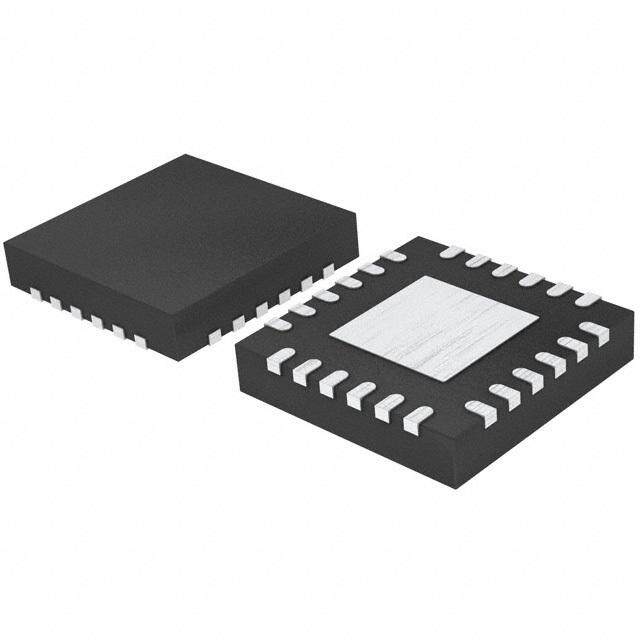
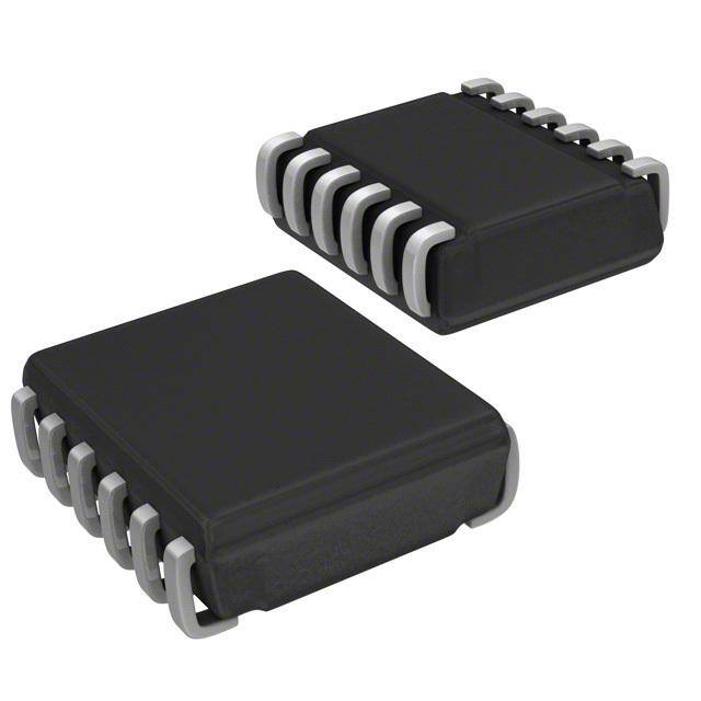
| 描述 | ADJ POS/NEG CHPUMP, 12TSOPJW |
| 产品分类 | |
| 品牌 | Skyworks Solutions Inc |
| 数据手册 | |
| 产品图片 | |
| 产品型号 | AAT3190ITP-T1 |
| rohs | 无铅 / 符合限制有害物质指令(RoHS)规范要求 |
| 产品系列 | - |
| 供应商器件封装 | 12-TSOPJW |
| 其它名称 | 863-1478-6 |
| 内部驱动器 | 是 |
| 包装 | 带卷 (TR) |
| 安装类型 | 表面贴装 |
| 封装/外壳 | 12-TFSOJ (0.094", 2.40mm 宽) |
| 工作温度 | -40°C ~ 85°C |
| 恒压 | - |
| 恒流 | - |
| 拓扑 | 切换式电容器(充电泵) |
| 标准包装 | 3,000 |
| 电压-电源 | 2.7 V ~ 5.5 V |
| 电压-输出 | 可调至 ±25V |
| 类型-初级 | 背光 |
| 类型-次级 | - |
| 输出数 | 2 |
| 频率 | 1MHz |





- 商务部:美国ITC正式对集成电路等产品启动337调查
- 曝三星4nm工艺存在良率问题 高通将骁龙8 Gen1或转产台积电
- 太阳诱电将投资9.5亿元在常州建新厂生产MLCC 预计2023年完工
- 英特尔发布欧洲新工厂建设计划 深化IDM 2.0 战略
- 台积电先进制程称霸业界 有大客户加持明年业绩稳了
- 达到5530亿美元!SIA预计今年全球半导体销售额将创下新高
- 英特尔拟将自动驾驶子公司Mobileye上市 估值或超500亿美元
- 三星加码芯片和SET,合并消费电子和移动部门,撤换高东真等 CEO
- 三星电子宣布重大人事变动 还合并消费电子和移动部门
- 海关总署:前11个月进口集成电路产品价值2.52万亿元 增长14.8%


PDF Datasheet 数据手册内容提取
DATA SHEET AAT3190 Positive/Negative Charge Pump for Voltage Bias General Description Features The AAT3190 charge pump controller provides the regu- • V Range: 2.7V to 5.5V IN lated positive and negative voltage biases required by • Adjustable ± Dual Charge Pump active matrix thin-film transistor (TFT) liquid-crystal dis- • Positive Supply Output Up to +25V plays (LCDs), charge-coupled device (CCD) sensors, and • Negative Supply Output Down to -25V organic light emitting diodes (OLEDs). Two low-power • Up to 30mA Output Current charge pumps convert input supply voltages ranging from • 1.0MHz Switching Frequency 2.7V to 5.5V into two independent output voltages. • <1.0μA Shutdown Current • Internal Power MOSFETs The dual low-power charge pumps independently regu- • Internally Controlled Soft Start late a positive (V ) and negative (V ) output voltage. POS NEG • Fast Transient Response These outputs use external diode and capacitor multi- • Ultra-Thin Solution (No Inductors) plier stages (as many stages as required) to regulate • -40°C to +85°C Temperature Range output voltages up to ±25V. Built-in soft-start circuitry • Available in 8-Pin MSOP or 12-Pin TSOPJW Package prevents excessive in-rush current during start-up. A high switching frequency enables the use of small exter- nal capacitors. The device’s shutdown feature discon- Applications nects the load from V and reduces quiescent current to IN • CCD Sensor Voltage Bias less than 1.0μA. • OLEDs The AAT3190 is available in a Pb-free MSOP-8 or • Passive-Matrix Displays TSOPJW-12 package and is specified over the -40°C to • Personal Digital Assistants (PDAs) +85°C operating temperature range. • TFT Active-Matrix LCDs Typical Application INPUT IN EN EN DRVN AAT3190 DRVP NEGATIVE FBN OUTPUT REF POSTIVE FBP OUTPUT GND Skyworks Solutions, Inc. • Phone [781] 376-3000 • Fax [781] 376-3100 • sales@skyworksinc.com • www.skyworksinc.com 1 202082A • Skyworks Proprietary Information • Products and Product Information are Subject to Change Without Notice. • June 21, 2012
DATA SHEET AAT3190 Positive/Negative Charge Pump for Voltage Bias Pin Description Pin # MSOP-8 TSOPJW-12 Symbol Function Positive charge pump feedback input. Regulates to 1.2V nominal. Connect feedback resis- 1 5 FBP tive divider to analog ground (GND). Enable input. When EN is pulled low, the device shuts off and draws only 1.0μA. When 2 4 EN high, it is in normal operation. Drive EN through an external resistor. Internal reference bypass terminal. Connect a 0.1μF capacitor from this terminal to ana- 3 3 REF log ground (GND). External load capability to 50μA. REF is disabled in shutdown. Negative charge pump regulator feedback input. Regulates to 0V nominal. Connect feed- 4 2 FBN back resistive divider to the reference (REF). 5 12 DRVP P ositive charge pump driver output. Output high level is V and low level is PGND. IN 6 8, 9, 10, 11 GND Ground. 7 7 DRVN Negative charge pump driver output. Output high level is V and low level is PGND. IN 8 1 VIN Input voltage: 2.7V to 5.5V. Pin Configuration MSOP-8 TSOPJW-12 (Top View) (Top View) FEBNP 12 1 2 87 DVIRNVN FRVBEINNF 123 111210 DGGRNNVDDP REF GND EN 4 9 GND 3 6 FBP 5 8 GND FBN 4 5 DRVP N/C 6 7 DRVN Skyworks Solutions, Inc. • Phone [781] 376-3000 • Fax [781] 376-3100 • sales@skyworksinc.com • www.skyworksinc.com 2 202082A • Skyworks Proprietary Information • Products and Product Information are Subject to Change Without Notice. • June 21, 2012
DATA SHEET AAT3190 Positive/Negative Charge Pump for Voltage Bias Absolute Maximum Ratings1 Symbol Description Value Units V Input Voltage -0.3 to 6 V IN V EN to GND -0.3 to 6 V EN V DRVN to GND -0.3V to (V + 0.3V) V N_CH IN V DRVP to GND -0.3V to (V + 0.3V) V P_CH IN Other Inputs REF, FBN, FBP to GND -0.3V to (V + 0.3V) V IN I Continuous Current Into DRVN, DRVP ±200 mA MAX All Other Pins ±10 T Operating Junction Temperature Range -40 to 150 °C J T Maximum Soldering Temperature (at leads, 10 sec.) 300 °C LEAD Thermal Information2 Symbol Description Value Units MSOP-8 150 Thermal Resistance °C/W JA TSOPJW-12 160 MSOP-83 667 P Maximum Power Dissipation (T = 25°C) mW D A TSOPJW-124 625 1. Stresses above those listed in Absolute Maximum Ratings may cause permanent damage to the device. Functional operation at conditions other than the operating conditions specified is not implied. Only one Absolute Maximum Rating should be applied at any one time. 2. Mounted on an FR4 board. 3. Derate 6.7mW/°C above 25°C. 4. Derate 6.25mW/°C above 25°C. Skyworks Solutions, Inc. • Phone [781] 376-3000 • Fax [781] 376-3100 • sales@skyworksinc.com • www.skyworksinc.com 3 202082A • Skyworks Proprietary Information • Products and Product Information are Subject to Change Without Notice. • June 21, 2012
DATA SHEET AAT3190 Positive/Negative Charge Pump for Voltage Bias Electrical Characteristics V = 5.0V, C = 0.1μF, T = -40°C to +85°C. Unless otherwise noted, typical values are T = 25°C. IN REF A A Symbol Description Conditions Min Typ Max Units V Input Supply Range 2.7 5.5 V IN V Rising 1.8 UVLO Input Under-Voltage Threshold IN V V Falling, 40mV Hysteresis (typ) 1.6 IN I Input Quiescent Supply Current V = 1.5V, V = -0.2V, No Load on DRVN and DRVP 400 800 μA IN FBP FBN I Shutdown Supply Current V = 0V 0.1 1.0 μA SD EN F Operating Frequency 0.8 1.0 1.2 MHz OSC Negative Low-Power Charge Pump V FBN Regulation Voltage -100 0 +100 mV FBN I FBN Input Bias Current V = -50mV -100 +100 nA FBN FBN R DRVN NCH On-Resistance 1.5 5.0 DSNCHN R MIN DRVN PCH On-Resistance V = 100mV, V = 4V 1.0 5.0 DSPCHMIN FBN IN R MAX DRVN PCH On-Resistance V = -100mV, V = 4V 20 k DSPCHMAX FBN IN Positive Low-Power Charge Pump V FBP Regulation Voltage 1.15 1.2 1.25 V FBP I FBP Input Bias Current V = 1.5V -60 +100 nA FBP FBP R DRVP PCH On-Resistance 1.0 5.0 DSPCHP R MIN DRVP NCH On-Resistance V = 1.15V, V = 4V 3 15 DSNCHMIN FBP IN R MAX DRVP NCH On-Resistance V = 1.25V, V = 4V 20 k DSNCHMIN FBP IN Reference Reference Voltage -2.0μA < I < 50μA 1.18 1.2 1.22 V REF Reference Under-Voltage V V Rising 0.8 V REF Threshold REF Logic Signals V Input Low Voltage 0.5 V IL V Input High Voltage 1.5 V IH I Enable Input Low Current V = 5.0V, F = 1.5V, F = -0.2V 1 μA IL IN BP BN I Enable Input High Current V = 5.0V, F = 1.5V, F = -0.2V 1 μA IH IN BP BN Thermal Limit Over-Temperature Shutdown T 140 °C SD Threshold Over-Temperature Shutdown T 15 °C HYST Hysteresis Skyworks Solutions, Inc. • Phone [781] 376-3000 • Fax [781] 376-3100 • sales@skyworksinc.com • www.skyworksinc.com 4 202082A • Skyworks Proprietary Information • Products and Product Information are Subject to Change Without Notice. • June 21, 2012
DATA SHEET AAT3190 Positive/Negative Charge Pump for Voltage Bias Typical Characteristics Quiescent Current vs. Temperature Switching Frequency vs. Temperature 350 1000 V = 1.5V FBP μnt (A) 330 VFBN = -0.2V Hz) 950 urre 310 cy (k 900 C n nt 290 ue e q c e 850 es 270 Fr ui Q 250 800 -40 -15 10 35 60 85 -40 -15 10 35 60 85 Temperature (°C) Temperature (°°C) Reference Voltage vs. Temperature Maximum V vs. V OUT IN (I = 5mA and 15mA) OUT 1.22 15 V) 12.5 I = 5mA e ( 1.21 V) 10 OP oltag age ( 27..555 IOP = 15mA e V 1.2 olt 0 enc ut V -2.-55 ION = 15mA Refer 1.19 Outp --71.05 I = 5mA -12.5 ON 1.18 -15 -40 -15 10 35 60 85 2.5 3 3.5 4 4.5 5 5.5 Temperature (°C) Input Voltage (V) Positive Output Voltage vs. Load Current Negative Output Voltage vs. Load Current (T = 85°°C) (T = 85°°C) 12.4 -6.5 V = 5.0V V = 5.0V IN IN 12.2 -6.75 -7 12 V) V) (OS 11.8 (EG -7.25 VP VN -7.5 11.6 -7.75 11.4 -8 0 10 20 30 40 0 10 20 30 40 I (mA) I (mA) POS NEG Skyworks Solutions, Inc. • Phone [781] 376-3000 • Fax [781] 376-3100 • sales@skyworksinc.com • www.skyworksinc.com 5 202082A • Skyworks Proprietary Information • Products and Product Information are Subject to Change Without Notice. • June 21, 2012
DATA SHEET AAT3190 Positive/Negative Charge Pump for Voltage Bias Typical Characteristics Positive Output Efficiency vs. Load Current Negative Output Efficiency vs. Load Current (VIN = 5.0V) (VIN = 5.0V) 80 80 V = 12.3V 25°C 85°C POS 70 70 85°C 25°C %) 60 %) 60 y ( y ( nc 50 nc 50 e e ci ci Effi 40 Effi 40 30 30 V = -7.3V NEG 20 20 0 10 20 30 40 0 10 20 30 40 I (mA) I (mA) POS NEG V Load Transient V Load Transient POS NEG 250 20 250 20 200 10 200 10 e) 150 0 e) 150 0 (bottom tracS(50mV/div) 105000 ---321000 (10mA/div)POSI (top trace (bottom tracG(50mV/div) 105000 ---321000 (10mA/div)NEGI (top trace O -50 -40 ) E -50 -40 ) P N V V -100 -50 -100 -50 -150 -60 -150 -60 Time (50µs/div) Time (50µs/div) AAT3190 Power-Up Sequence AAT3190-1 Power-Up Sequence 20 4 20 4 Enable Enable 16 2 16 2 V) 12 0 V) 12 0 V and V POSNEGbottom traces, -4048 VVPNOESG ----8642 (top trace, V)Enable V and V POSNEGbottom traces, -4048 VVPNOESG ----8642 (top trace, V)Enable ( ( -8 -10 -8 -10 -12 -12 -12 -12 Time (500µs/div) Time (500µs/div) Skyworks Solutions, Inc. • Phone [781] 376-3000 • Fax [781] 376-3100 • sales@skyworksinc.com • www.skyworksinc.com 6 202082A • Skyworks Proprietary Information • Products and Product Information are Subject to Change Without Notice. • June 21, 2012
DATA SHEET AAT3190 Positive/Negative Charge Pump for Voltage Bias Typical Characteristics Output Ripple Positive Output Voltage vs. Load Current (V = 12.3V; I = 5mA; V = 7.2V; I = 10mA) (T = 25°°C) POS POS NEG NEG A 12.4 V = 5.0V IN V 12.2 POS (10mV/div) V) 12 (S O VP 11.8 11.6 V NEG 11.4 (10mV/div) 0 5 10 15 20 25 30 35 40 Time (500ns/div) IPOS (mA) Negative Output Voltage vs. Load Current AAT3190 Reference Under-Voltage Threshold (T = 25°°C) A (120µF capacitor placed across REF to limit rate of rise of REF for test purposes only) -6.5 V = 5.0V IN SHDN -6.75 (2V/div) -7 V) (EG -7.25 R(0E.2FV /div) N 0.5V V -7.5 DRVN -7.75 (2V/div) -8 0 10 20 30 40 INEG (mA) Time (500ns/div) Skyworks Solutions, Inc. • Phone [781] 376-3000 • Fax [781] 376-3100 • sales@skyworksinc.com • www.skyworksinc.com 7 202082A • Skyworks Proprietary Information • Products and Product Information are Subject to Change Without Notice. • June 21, 2012
DATA SHEET AAT3190 Positive/Negative Charge Pump for Voltage Bias Functional Block Diagram IN DRVP UVLO EN Control DRVN Reference + FBP Oscillator - Over- Band Temperature Gap REF Protection Ref. - FBN GND + Functional Description Positive Charge Pump During the first half-cycle, the N-channel MOSFET turns Dual Charge Pump Regulators on and charges the flying capacitor C4 (Figure 2). During the second half-cycle, the N-channel MOSFET turns off The AAT3190 provides low-power regulated output volt- and the P-channel MOSFET turns on, level shifting C4 by ages from two individual charge pumps. Using a single the input voltage. This connects C4 in parallel with the stage, the first charge pump inverts the supply voltage reservoir capacitor C5. If the voltage across C5 plus a (V ) and provides a regulated negative output voltage. IN diode drop is less than the level shifted flying capacitor The second charge pump doubles V and provides a IN (C4 + V ), charge is transferred from C4 to C5 until the regulated positive output voltage. These outputs use IN diode turns off. external Schottky diodes and capacitor multiplier stages (as many as required) to regulate up to ±25V. A con- Voltage Reference stant switching frequency of 1MHz minimizes the output ripple and capacitor size. The voltage reference is a simple band gap with an out- put voltage equal to V + K*V. The band gap reference BE T Negative Charge Pump amplifier has an additional compensation capacitor from the negative input to the output. This capacitor serves to During the first half-cycle, the P-channel MOSFET turns slow down the circuit during startup and soft starts the on and the flying capacitor C7 charges to V minus a IN voltage reference and the regulator output from over- diode drop (Figure 1). During the second half-cycle, the shoot. The reference circuit amplifier also increases the P-channel MOSFET turns off and the N-channel MOSFET overall PSRR of the device. An 80k resistor serves to turns on, level shifting C7. This connects C7 in parallel isolate and buffer the amplifier from a small internal filter with the output reservoir capacitor C10. If the voltage capacitor and an optional large external filter capacitor. across C10 minus a diode drop is less than the voltage across C7, current flows from C7 to C10 until the diode turns off. Skyworks Solutions, Inc. • Phone [781] 376-3000 • Fax [781] 376-3100 • sales@skyworksinc.com • www.skyworksinc.com 8 202082A • Skyworks Proprietary Information • Products and Product Information are Subject to Change Without Notice. • June 21, 2012
DATA SHEET AAT3190 Positive/Negative Charge Pump for Voltage Bias IN C7 1/2 A4 OSC DRVN CTL BAT54SDW FBN R1 VON = -(R1/R2) x VREF VON R2 C10 VREF AAT3190 1.2V C2 GND Figure 1: Negative Charge Pump Block Diagram. IN VIN 1/2 A3 C4 OSC CTL DRVP BAT54SDW FBP R3 VOP VOP = (1+R3/R4) x VREF VREF R4 C5 1.2V AAT3190 GND Figure 2: Positive Charge Pump Block Diagram. Enable and Start-up AAT3190 start-up sequence ramps up the V output OP 200μs after the V output is present. The AAT3190-1 ON The AAT3190 is disabled by pulling the EN pin low. The ramps up the positive supply before the negative supply. threshold levels lie between 0.5V and 1.5V. Even though the quiescent current of the IC during shutdown is less Over-Temperature Protection than 1μA, the positive output voltage (V ) and any load OP current associated with it does not disappear without the A logic control circuit will shut down both charge pumps complete removal of the input voltage. This is due to the in the case of an over-temperature condition. fact that with no switching of the DRVP pin, the input voltage simply forward biases the Schottky diodes asso- Under-Voltage Lockout ciated with the V charge pump, providing a path for OP load current to be drawn from the input voltage. A UVLO circuit disables the AAT3190 when the input volt- age supply is lower than 1.8V nominal. Depending on the application, the supplies must be sequenced properly to avoid damage or latch-up. The Skyworks Solutions, Inc. • Phone [781] 376-3000 • Fax [781] 376-3100 • sales@skyworksinc.com • www.skyworksinc.com 9 202082A • Skyworks Proprietary Information • Products and Product Information are Subject to Change Without Notice. • June 21, 2012
DATA SHEET AAT3190 Positive/Negative Charge Pump for Voltage Bias Design Procedure V OP and Component Selection The positive output voltage is set by way of a resistive divider from the output (V ) to the FBP and ground pin. Output Voltage OP Limiting the size of R4 reduces the effect of the FBP bias The number of charge pump stages required for a given current. For less than 0.1% error, limit R4 to less than output varies with the input voltage applied. The number 12k. of stages required can be estimated by: V 1.2V I = REF = = 100μA V - V PGM R4 12kΩ n = OP IN p V - 2V IN F I 0.1μA FBP = = 0.1% I 100μA for the positive output and PGM V n = ON Once R4 has been determined, solve for R3: n 2V - V F IN ⎛ V ⎞ R3 = R4 · O - 1 for the negative output. ⎝V ⎠ REF When solving for n and n , round up the solution to the p n next highest integer to determine the number of stages Flying and Output Capacitor required. The flying capacitor minimum value is limited by the output power requirement, while the maximum value is V ON set by the bandwidth of the power supply. If C is too FLY The negative output voltage is adjusted by a resistive small, the output may not be able to deliver the power divider from the output (V ) to the FBN and REF pin. demanded, while too large of a capacitor may limit the ON bandwidth and time required to recover from load and The maximum reference voltage current is 50μA; there- line transients. A 0.1μF X7R or X5R ceramic capacitor is fore, the minimum allowable value for R2 of Figure 1 is typically used. The voltage rating of the flying and res- 24k. It is best to select the smallest value possible for ervoir output capacitors varies with the number of R2, as this will keep R1 to a minimum. This limits errors charge pump stages. The reservoir output capacitor due to the FBN input bias current. The FBN input has a should be roughly 10 times the flying capacitor. Use maximum input bias current of 100nA. Using the full larger capacitors for reduced output ripple. 50μA reference current for programming V : ON V 1.2 Positive Output Capacitor I = REF = = 50μA PGM R2 24.1k Voltage Ratings The absolute steady-state maximum output voltage will limit the error due to the input bias current at FBN (neglecting the internal R drop of the internal to less than 0.2%: DS(ON) MOSFETs) for the nth stage is: I 0.1μA FBN = = 0.2% V = (n + 1) · V - 2 · n · V I 50μA BULK(n) IN FWD PGM where V is the estimated forward drop of the Schottky With R2 selected, R1 can be determined: FWD diode. This is also the voltage rating required for the nth V · R2 bulk capacitor in the positive output charge pump. R1 = NEG -V REF The voltage rating for the nth flying capacitor in the positive stage is: V = V - V FLY(n) BULK(n + 1) FWD where V is the input voltage (see Table 1). BULK(0) Skyworks Solutions, Inc. • Phone [781] 376-3000 • Fax [781] 376-3100 • sales@skyworksinc.com • www.skyworksinc.com 10 202082A • Skyworks Proprietary Information • Products and Product Information are Subject to Change Without Notice. • June 21, 2012
DATA SHEET AAT3190 Positive/Negative Charge Pump for Voltage Bias Input Capacitors V = 5.0V, V = 0.3V IN FWD Stages (n) V V BULK(n) FLY(n) Input Capacitor 1 9.4V 4.7V 2 13.8V 9.1V The primary function of the input capacitor is to provide a 3 18.2V 13.5V low impedance loop for the edges of pulsed current drawn 4 22.6V 17.9V by the IC. A low ESL X7R or X5R type ceramic capacitor 5 27.0V 22.3V is ideal for this function. The size required will vary 6 31.4V 26.7V depending on the load, output voltage, and input voltage Table 1: Positive Output Capacitor Voltages. characteristics. Typically, the input capacitor should be 5 to 10 times the flying capacitor. If the source impedance of the input supply is high, a larger capacitor may be Negative Output Capacitor required. To minimize stray inductance, the capacitor Voltage Ratings should be placed as closely as possible to the IC. This keeps the high frequency content of the input current The absolute steady-state maximum output voltage localized, minimizing radiated and conducted EMI. (neglecting the internal R drop of the internal DS(ON) MOSFETs) for the nth stage is: Rectifier Diodes V = -n · V + 2 · n · V For the rectifiers, use Schottky diodes with a voltage rat- BULK(n) IN FWD ing of 1.5 times the input voltage. The maximum steady- state voltage seen by the rectifier diodes for both the This is also the voltage rating required for the nth bulk positive and negative charge pumps (regardless of the capacitor in the negative output charge pump. number of stages) is: The voltage rating for the nth flying capacitor in the negative stage (see Table 2) is: V = V - V REVERSE IN F V = V - V FLY(n) FWD BULK(n) The BAT54S dual Schottky is offered in a SOT23 package that provides a convenient pin-out for the voltage dou- VIN = 5.0V, VFWD = 0.3V bler configuration. The BAT54SDW quad Schottky in a Stages (n) V V SOT363 (2x2mm) package is a good choice for multiple- BULK(n) FLY(n) stage charge pump configuration (see Figure 3, Evaluation 1 -4.4V 4.7V 2 -8.8V 9.1V Board Schematic). 3 -13.2V 13.5V 4 -17.6V 17.9V PC Board Layout 5 -22.0V 22.3V 6 -26.4V 26.7V The input and reference capacitor should be placed as close to the IC as possible. Place the programming resis- Table 2: Negative Output Capacitor Voltages. tors (R1-R4) close to the IC, minimizing trace length to FBN and FBP. Figures 4 and 5 display the evaluation board layout with the TSOPJW-12 package. Single Output Operation If only one of the two channels is needed, it is possible to disable either output. Connect the respective FB pin to V to disable the output (e.g., connect FBN to V in IN IN order to disable the negative output). Skyworks Solutions, Inc. • Phone [781] 376-3000 • Fax [781] 376-3100 • sales@skyworksinc.com • www.skyworksinc.com 11 202082A • Skyworks Proprietary Information • Products and Product Information are Subject to Change Without Notice. • June 21, 2012
DATA SHEET AAT3190 Positive/Negative Charge Pump for Voltage Bias V IN A4 A3 BAT54SDW C8 BAT54SDW 0.1μF C9 0.1μF R5 R3 205K U1 C21 56.2k 1 VIN DRVP 12 C7 1μF 2 FBN GND 11 0.1μF C1μ2F0 C10 0.1μF 3 REF GND 10 2R42.1k 4 EN GND 9 VOP 5 FBP GND 8 C1 C19 VON 6 N/C DRVN 7 4.7μF 1μF C2 C22 1R319k 0.1μF R6.402k AAT3190ITP 1μF GND GND C19, C20, C21, C22 Murata GRM39X5R105K16 1μF 16V X5R 0603 EN C7, C8, C9, C10 Taiyo Yuden EMK107BJ104MA 0.1μF 16V X7R 0603 C1 Taiyo Yuden JMK212BJ475MG 4.7μF 6.3V X5R 0805 Figure 3: AAT3190 Evaluation Board Schematic (shown with two stages) V = 12V, V = -7V. OP ON Figure 4: AAT3190 Evaluation Board Top Side. Figure 5: AAT3190 Evaluation Board Bottom Side. Skyworks Solutions, Inc. • Phone [781] 376-3000 • Fax [781] 376-3100 • sales@skyworksinc.com • www.skyworksinc.com 12 202082A • Skyworks Proprietary Information • Products and Product Information are Subject to Change Without Notice. • June 21, 2012
DATA SHEET AAT3190 Positive/Negative Charge Pump for Voltage Bias Ordering Information Package Power-Up Sequence Marking1 Part Number (Tape and Reel)2 MSOP-8 -, + JDXYY AAT3190IKS-T1 TSOPJW-12 -, + JDXYY AAT3190ITP-T1 TSOPJW-12 +, - LKXYY AAT3190ITP-1-T1 Skyworks Green™ products are compliant with all applicable legislation and are halogen-free. For additional information, refer to Skyworks Definition of Green™, document number SQ04-0074. Package Information MSOP-8 4° ± 4° 1.95 BSC ±3.00 0.10 ±4.90 0.10 0.60 ± 0.20 F PIN 1 RE 0.254 BSC 0.95 E 0.155 ± 0.075 N A 3.00 ± 0.10 PL E 10° ± 5° UG A G ±0.95 0.15 ±0.85 0.10 0.075 ± 0.075 0.65 BSC 0.30 ± 0.08 All dimensions in millimeters. 1. XYY = assembly and date code. 2. Sample stock is generally held on part numbers listed in BOLD. Skyworks Solutions, Inc. • Phone [781] 376-3000 • Fax [781] 376-3100 • sales@skyworksinc.com • www.skyworksinc.com 13 202082A • Skyworks Proprietary Information • Products and Product Information are Subject to Change Without Notice. • June 21, 2012
DATA SHEET AAT3190 Positive/Negative Charge Pump for Voltage Bias TSOPJW-12 0.20 + 0.10 - 0.05 0 0 1 2 0. 0. ± ± 0 5 4 8 2. 2. 0.50 BSC0.50 BSC0.50 BSC0.50 BSC0.50 BSC 7° NOM 0.04 REF 3.00 ± 0.10 5 0 ±0.9625 0.0375 + 0.10 1.00 - 0.065 ±0.15 0. 0.055 ± 0.045 0.010 4° ± 4° 0.45 ± 0.15 2.75 ± 0.25 All dimensions in millimeters. Copyright © 2012 Skyworks Solutions, Inc. All Rights Reserved. Information in this document is provided in connection with Skyworks Solutions, Inc. (“Skyworks”) products or services. These materials, including the information contained herein, are provided by Skyworks as a service to its customers and may be used for informational purposes only by the customer. Skyworks assumes no responsibility for errors or omissions in these materials or the information contained herein. Sky- works may change its documentation, products, services, specifi cations or product descriptions at any time, without notice. Skyworks makes no commitment to update the materials or information and shall have no responsibility whatsoever for confl icts, incompatibilities, or other diffi culties arising from any future changes. No license, whether express, implied, by estoppel or otherwise, is granted to any intellectual property rights by this document. Skyworks assumes no liability for any materials, products or information provided here- under, including the sale, distribution, reproduction or use of Skyworks products, information or materials, except as may be provided in Skyworks Terms and Conditions of Sale. THE MATERIALS, PRODUCTS AND INFORMATION ARE PROVIDED “AS IS” WITHOUT WARRANTY OF ANY KIND, WHETHER EXPRESS, IMPLIED, STATUTORY, OR OTHERWISE, INCLUDING FITNESS FOR A PARTICULAR PURPOSE OR USE, MERCHANTABILITY, PERFORMANCE, QUALITY OR NON-INFRINGEMENT OF ANY INTELLECTUAL PROPERTY RIGHT; ALL SUCH WARRANTIES ARE HEREBY EXPRESSLY DISCLAIMED. SKYWORKS DOES NOT WARRANT THE ACCURACY OR COMPLETENESS OF THE INFORMATION, TEXT, GRAPHICS OR OTHER ITEMS CONTAINED WITHIN THESE MATERIALS. SKYWORKS SHALL NOT BE LIABLE FOR ANY DAMAGES, IN- CLUDING BUT NOT LIMITED TO ANY SPECIAL, INDIRECT, INCIDENTAL, STATUTORY, OR CONSEQUENTIAL DAMAGES, INCLUDING WITHOUT LIMITATION, LOST REVENUES OR LOST PROFITS THAT MAY RESULT FROM THE USE OF THE MATERIALS OR INFORMATION, WHETHER OR NOT THE RECIPIENT OF MATERIALS HAS BEEN ADVISED OF THE POSSIBILITY OF SUCH DAMAGE. Skyworks products are not intended for use in medical, lifesaving or life-sustaining applications, or other equipment in which the failure of the Skyworks products could lead to personal injury, death, physical or en- vironmental damage. Skyworks customers using or selling Skyworks products for use in such applications do so at their own risk and agree to fully indemnify Skyworks for any damages resulting from such improper use or sale. Customers are responsible for their products and applications using Skyworks products, which may deviate from published specifi cations as a result of design defects, errors, or operation of products outside of pub- lished parameters or design specifi cations. Customers should include design and operating safeguards to minimize these and other risks. Skyworks assumes no liability for applications assistance, customer product design, or damage to any equipment resulting from the use of Skyworks products outside of stated published specifi cations or parameters. Skyworks, the Skyworks symbol, and “Breakthrough Simplicity” are trademarks or registered trademarks of Skyworks Solutions, Inc., in the United States and other countries. Third-party brands and names are for identifi cation purposes only, and are the property of their respective owners. Additional information, including relevant terms and conditions, posted at www.skyworksinc.com, are incorporated by reference. Skyworks Solutions, Inc. • Phone [781] 376-3000 • Fax [781] 376-3100 • sales@skyworksinc.com • www.skyworksinc.com 14 202082A • Skyworks Proprietary Information • Products and Product Information are Subject to Change Without Notice. • June 21, 2012
 Datasheet下载