ICGOO在线商城 > AAT2153IVN-0.6-T1
- 型号: AAT2153IVN-0.6-T1
- 制造商: SKYWORKS
- 库位|库存: xxxx|xxxx
- 要求:
| 数量阶梯 | 香港交货 | 国内含税 |
| +xxxx | $xxxx | ¥xxxx |
查看当月历史价格
查看今年历史价格
AAT2153IVN-0.6-T1产品简介:
ICGOO电子元器件商城为您提供AAT2153IVN-0.6-T1由SKYWORKS设计生产,在icgoo商城现货销售,并且可以通过原厂、代理商等渠道进行代购。 提供AAT2153IVN-0.6-T1价格参考以及SKYWORKSAAT2153IVN-0.6-T1封装/规格参数等产品信息。 你可以下载AAT2153IVN-0.6-T1参考资料、Datasheet数据手册功能说明书, 资料中有AAT2153IVN-0.6-T1详细功能的应用电路图电压和使用方法及教程。
| 参数 | 数值 |
| 产品目录 | 集成电路 (IC)半导体 |
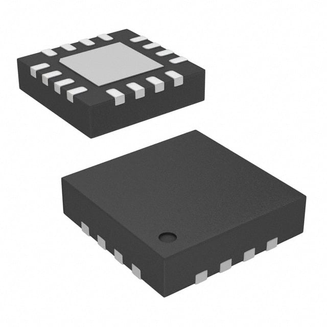
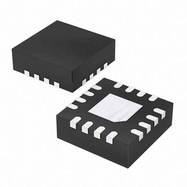
| 描述 | IC REG BUCK SYNC ADJ 2.5A 16QFN稳压器—开关式稳压器 2.5A Low Noise Buck Converter |
| 产品分类 | |
| 品牌 | Skyworks Solutions, Inc. |
| 产品手册 | |
| 产品图片 |
|
| rohs | 符合RoHS无铅 / 符合限制有害物质指令(RoHS)规范要求 |
| 产品系列 | 电源管理 IC,稳压器—开关式稳压器,Skyworks Solutions, Inc. AAT2153IVN-0.6-t1SwitchReg™ |
| 数据手册 | |
| 产品型号 | AAT2153IVN-0.6-t1 |
| PWM类型 | 电流模式 |
| 产品种类 | 稳压器—开关式稳压器 |
| 供应商器件封装 | 16-QFN(3x3) |
| 其它名称 | 863-1499-6 |
| 包装 | Digi-Reel® |
| 同步整流器 | 是 |
| 商标 | Skyworks Solutions, Inc. |
| 安装类型 | 表面贴装 |
| 安装风格 | SMD/SMT |
| 封装 | Reel |
| 封装/外壳 | 16-VFQFN 裸露焊盘 |
| 封装/箱体 | QFN-33-16 |
| 工作温度 | -40°C ~ 85°C |
| 工作温度范围 | - 40 C to + 85 C |
| 工厂包装数量 | 1500 |
| 开关频率 | 1.4 MHz |
| 最大工作温度 | + 85 C |
| 最大输入电压 | 5.5 V |
| 最小工作温度 | - 40 C |
| 最小输入电压 | 2.7 V |
| 标准包装 | 1 |
| 电压-输入 | 2.7 V ~ 5.5 V |
| 电压-输出 | 0.6 V ~ 5.5 V |
| 电流-输出 | 2.5A |
| 电源电压-最小 | 2.7 V |
| 类型 | Voltage Converter |
| 负载调节 | 0.5 % |
| 输出数 | 1 |
| 输出电压 | Adj |
| 输出电流 | 2.5 A |
| 输出端数量 | 1 Output |
| 输出类型 | 可调式 |
| 频率-开关 | 1.4MHz |
.jpg)

PDF Datasheet 数据手册内容提取
DATA SHEET AAT2153 2.5A Low-Noise,Step-Down Converter General Description Features The AAT2153 SwitchReg is a 2.5A step-down converter • 2.5A Maximum Output Current with an input voltage range of 2.7V to 5.5V and an • Input Voltage: 2.7V to 5.5V adjustable output voltage from 0.6V to V . The 1.4MHz • Output Voltage: 0.6V to V IN IN switching frequency enables the use of small external • Up to 95% Efficiency components. The small footprint and high efficiency make • Low Noise Light Load Mode the AAT2153 an ideal choice for portable applications. • 42μA No Load Quiescent Current • No External Compensation Required The AAT2153 delivers 2.5A maximum output current • 1.4MHz Switching Frequency while consuming only 42μA of no-load quiescent current. • 100% Duty Cycle Low-Dropout Operation Ultra-low R integrated MOSFETs and 100% duty DS(ON) • Internal Soft Start cycle operation make the AAT2153 an ideal choice for • Over-Temperature and Current Limit Protection high output voltage, high current applications which • <1μA Shutdown Current require a low dropout threshold. • 16-Pin 3x3mm QFN Package The AAT2153 provides excellent transient response and • Temperature Range: -40°C to +85°C high output accuracy across the operating range. No external compensation components are required. Applications The AAT2153 maintains high efficiency throughout the • Cellular Phones load range. The AAT2153’s unique architecture produces • Digital Cameras reduced ripple and spectral noise. Over-temperature and • Hard Disk Drives short-circuit protection safeguard the AAT2153 and sys- • MP3 Players tem components from damage. • PDAs and Handheld Computers • Portable Media Players The AAT2153 is available in a Pb-free, space-saving • USB Devices 16-pin 3x3mm QFN package. The product is rated over an operating temperature range of -40°C to +85°C. Typical Application U1 3.3V AAT2153 2.5V 12 4 VP FB 11 15 R3 VP LX 187k 10 14 L1 VP LX 2.2µH C1 7 13 10µF EN LX 9 16 VCC N/C R4 6 3 N/C PGND 59k C3 8 2 N/C PGND 22µF 5 1 SGND PGND Skyworks Solutions, Inc. • Phone [781] 376-3000 • Fax [781] 376-3100 • sales@skyworksinc.com • www.skyworksinc.com 1 202010A • Skyworks Proprietary Information • Products and Product Information are Subject to Change Without Notice. • May 28, 2012
DATA SHEET AAT2153 2.5A Low-Noise,Step-Down Converter Pin Descriptions Pin # Symbol Function 1, 2, 3 PGND Main power ground return pin. Connect to the output and input capacitor return. (See board layout rules.) Feedback input pin. For an adjustable output, connect an external resistive divider to this pin. For fi xed 4 FB output voltage versions, FB is the output pin of the converter. 5 SGND Signal ground. Connect the return of all small signal components to this pin. (See board layout rules.) 6, 8, 16 N/C Not internally connected. Enable input pin. A logic high enables the converter; a logic low forces the AAT2153 into shutdown mode 7 EN reducing the supply current to less than 1μA. The pin should not be left fl oating. 9 VCC Bias supply. Supplies power for the internal circuitry. Connect to input power. 10, 11, 12 VP Input supply voltage for the converter power stage. Must be closely decoupled to PGND. Connect inductor to these pins. Switching node internally connected to the drain of both high- and low-side 13, 14, 15 LX MOSFETs. EP Exposed paddle (bottom); connect to PGND directly beneath package. Pin Configuration QFN33-16 (Top View) N /CLXLXLX 16 15 14 13 PGND VP 1 12 PGND VP 2 11 PGND 3 10 VP FB 4 9 VCC 5 6 7 8 SNEN GC/NC/ N D Skyworks Solutions, Inc. • Phone [781] 376-3000 • Fax [781] 376-3100 • sales@skyworksinc.com • www.skyworksinc2.c1om53 . 2 0 0 8 . 1 2 . 1 .1 2 202010A • Skyworks Proprietary Information • Products and Product Information are Subject to Change Without Notice. • May 28, 2012
DATA SHEET AAT2153 2.5A Low-Noise,Step-Down Converter Absolute Maximum Ratings1 Symbol Description Value Units V , V V , V to GND 6 V CC P CC P V LX to GND -0.3 to V + 0.3 V LX P V FB to GND -0.3 to V + 0.3 V FB CC V EN to GND -0.3 to -6 V EN T Operating Junction Temperature Range -40 to150 °C J Thermal Characteristics Symbol Description Value Units Maximum Thermal Resistance 50 °C/W JA Maximum Thermal Resistance 4.2 °C/W JC P Maximum Power Dissipation (T = 25°C)2, 3 2.0 W D A Recommended Operating Conditions Symbol Description Value Units T Ambient Temperature Range -40 to 85 °C A 1. Stresses above those listed in Absolute Maximum Ratings may cause damage to the device. Functional operation at conditions other than the operating conditions specified is not implied. Only one Absolute Maximum Rating should be applied at any one time. 2. Mounted on a demo board (FR4, in still air). Exposed pad must be mounted to PCB. 3. Derate 20mW/°C above 25°C. Skyworks Solutions, Inc. • Phone [781] 376-3000 • Fax [781] 376-3100 • sales@skyworksinc.com • www.skyworksinc.com 3 202010A • Skyworks Proprietary Information • Products and Product Information are Subject to Change Without Notice. • May 28, 2012
DATA SHEET AAT2153 2.5A Low-Noise,Step-Down Converter Electrical Characteristics1 V = 3.6V; T = -40°C to +85°C, unless otherwise noted. Typical values are T = 25°C. IN A A Symbol Description Conditions Min Typ Max Units V Input Voltage 2.7 5.5 V IN V Output Voltage Range 0.6 V V OUT IN V Rising 2.7 V IN V UVLO Threshold Hysteresis 250 mV UVLO V Falling 1.8 V IN V Output Voltage Tolerance I = 0A to 2.5A, V = 2.7V to 5.5V -3.0 3.0 % OUT OUT IN I Quiescent Current No Load 42 90 μA Q I Shutdown Current V = GND 1.0 μA SHDN EN I Current Limit 2.8 3.5 A LIM R High Side Switch On-Resistance 0.120 DS(ON)H R Low Side Switch On-Resistance 0.085 DS(ON)L V Load Regulation I = 0A to 2.5A 0.5 % LOADREG LOAD V /V Line Regulation V = 2.7V to 5.5V 0.2 %/V LINEREG IN IN Feedback Threshold Voltage Accuracy V No Load, T = 25°C 0.591 0.60 0.609 V FB (Adjustable Version) A I FB Leakage Current V = 1.0V 0.2 μA FB OUT F Internal Oscillator Frequency 1.12 1.4 1.68 MHz OSC From Enable to Output Regulation; T Start-Up Time 150 μs S C = 100pF FF T Over-Temperature Shutdown Threshold 140 °C SD T Over-Temperature Shutdown Hysteresis 15 °C HYS EN V Enable Threshold Low 0.6 V IL V Enable Threshold High 1.4 V IH I Enable Leakage Current V = V = 5.5V -1.0 1.0 μA EN IN EN 1. The AAT2153 is guaranteed to meet performance specifications over the -40°C to +85°C operating temperature range and is assured by design, characterization, and correla- tion with statistical process controls. Skyworks Solutions, Inc. • Phone [781] 376-3000 • Fax [781] 376-3100 • sales@skyworksinc.com • www.skyworksinc2.c1om53 . 2 0 0 8 . 1 2 . 1 .1 4 202010A • Skyworks Proprietary Information • Products and Product Information are Subject to Change Without Notice. • May 28, 2012
DATA SHEET AAT2153 2.5A Low-Noise,Step-Down Converter Typical Characteristics Efficiency vs. Output Current Load Regulation (V = 3.3V) (V = 3.3V) OUT OUT 100 1.0 90 0.8 VIN = 5.0V 80 %) 0.6 VVIN == 44..52VV %) 70 n ( 0.4 IN ncy ( 5600 ulatio 00..02 Efficie 342000 VVIN == 54..05VV oad Reg ---000...642 10 VIN = 4.2V L -0.8 IN 0 -1.0 0 1 10 100 1000 10000 0.1 1 10 100 1000 10000 Output Current (mA) Output Current (mA) Efficiency vs. Output Current Load Regulation (V = 1.8V) (V = 1.8V) OUT OUT 100 1.0 90 0.8 VIN = 4.2V 80 %) 0.6 VIN = 3.6V %) 70 n ( 0.4 VIN = 2.7V ncy ( 5600 ulatio 00..02 e g Effici 342000 VVIN == 43..26VV oad Re ---000...642 10 VIN = 2.7V L -0.8 IN 0 -1.0 0 1 10 100 1000 10000 0.1 1 10 100 1000 10000 Output Current (mA) Output Current (mA) Efficiency vs. Output Current Load Regulation (V = 1.2V) (V = 1.2) OUT OUT 100 1.0 V = 4.2V 90 0.8 IN 80 %) 0.6 VVIN == 32..67VV %) 70 n ( 0.4 IN ncy ( 5600 ulatio 00..02 Efficie 3400 V = 4.2V d Reg --00..42 20 VIN = 3.6V oa -0.6 10 VIN = 2.7V L -0.8 IN 0 -1.0 0 1 10 100 1000 10000 0.1 1 10 100 1000 10000 Output Current (mA) Output Current (mA) Skyworks Solutions, Inc. • Phone [781] 376-3000 • Fax [781] 376-3100 • sales@skyworksinc.com • www.skyworksinc.com 5 202010A • Skyworks Proprietary Information • Products and Product Information are Subject to Change Without Notice. • May 28, 2012
DATA SHEET AAT2153 2.5A Low-Noise,Step-Down Converter Typical Characteristics Quiescent Current vs. Input Voltage Output Voltage vs. Temperature (V = 1.8V; No Load) (V = 1.8V; I = 2.5A) OUT OUT OUT 80 1.5 A) 70 %) 1.0 Current (µ 456000 2855°°CC age Error ( --0010....0505 nt 30 olt -1.5 Quiesce 2100 -40°C utput V ---322...050 O 0 -3.5 2.7 2.9 3.1 3.3 3.5 3.7 3.9 4.1 4.3 4.5 4.7 4.9 5.1 5.3 5.5 -40 -30 -20 -10 0 10 20 30 40 50 60 70 80 90 Input Voltage (V) Temperature (°C) Output Voltage vs. Input Voltage Switching Frequency vs. Temperature (VOUT = 1.8V; IOUT = 1A) (VOUT = 1.8V; IOUT = 2.5A) %) 1 1.82 85°C n ( 1.81 o 0 e (V) 11..7890 Variati -1 Voltag 11..7778 25°C uency --32 put 1.76 -40°C Freq -4 ut 1.75 g O n -5 1.74 hi c 1.73 wit -6 2.7 2.9 3.1 3.3 3.5 3.7 3.9 4.1 4.3 4.5 4.7 4.9 5.1 5.3 5.5 S -40 -30 -20 -10 0 10 20 30 40 50 60 70 80 90 Input Voltage (V) Temperature (°C) Load Transient Response Load Transient Response (V = 1.8V) (V = 1.8V; C = 100pF) OUT OUT FF d) 0.20 2.4 d) 0.20 2.4 e e pl 0.10 2.2 pl 0.10 2.2 u u oltage (AC co(top)(mV) ---0000....03210000 1112....4680 (bottom) (AOutput Curre oltage (AC co(top)(mV)---0000....03210000 1112....4680 (bottom) (AOutput Curre V -0.40 1.2 )n V -0.40 1.2 )n put -0.50 1.0 t put -0.50 1.0 t Out -0.60 0.8 Out -0.60 0.8 Time (100µs/div) Time (100µs/div) Skyworks Solutions, Inc. • Phone [781] 376-3000 • Fax [781] 376-3100 • sales@skyworksinc.com • www.skyworksinc2.c1om53 . 2 0 0 8 . 1 2 . 1 .1 6 202010A • Skyworks Proprietary Information • Products and Product Information are Subject to Change Without Notice. • May 28, 2012
DATA SHEET AAT2153 2.5A Low-Noise,Step-Down Converter Typical Characteristics Load Transient Response Load Transient Response (I = 1A to 2.5A; V = 1.8V; R1 = 0Ω; C = 2x22μF) (I = 1A to 2.5A; V = 1.8V; R1 = 10Ω; C = 22μF) OUT OUT OUT OUT OUT OUT 2.0 2.0 L L V) 1.9 o V) 1.9 o p) ( 1.8 ad C p) ( 1.8 ad C e (to 1.7 urre e (to 1.7 urre oltag 1.6 23 nt (b oltag 1.6 32 nt (b V o V o ut 1 tto ut 1 tto p m p m Out 0 ) (A Out 0 ) (A ) ) Time (100μs/div) Time (100μs/div) Load Transient Response Load Transient Response (I = 250mA to 2.5A; V = 1.8V; R1 = 0Ω; C = 2x22μF) (I = 250mA to 2.5A; V = 1.8V; R1 = 10Ω; C = 22μF) OUT OUT OUT OUT OUT OUT 2.0 2.0 L L V) 1.9 o V) 1.9 o p) ( 1.8 ad C p) ( 1.8 ad C e (to 1.7 urre e (to 1.7 urre oltag 1.6 32 nt (b oltag 1.6 23 nt (b V o V o ut 1 tto ut 1 tto p m p m Out 0 ) (A Out 0 ) (A ) ) Time (100μs/div) Time (100μs/div) Load Transient Response Load Transient Response (I = 100mA to 2.5A; V = 1.8V; R1 = 0Ω; C = 2x22μF) (I = 100mA to 2.5A; V = 1.8V; R1 = 10Ω; C = 22μF) OUT OUT OUT OUT OUT OUT 2.0 2.0 L L V) 1.9 o V) 1.9 o p) ( 1.8 ad C p) ( 1.8 ad C e (to 1.7 urre e (to 1.7 urre Voltag 1.6 23 nt (bo Voltag 1.6 23 nt (bo ut 1 tto ut 1 tto p m p m Out 0 ) (A Out 0 ) (A ) ) Time (100μs/div) Time (100μs/div) Skyworks Solutions, Inc. • Phone [781] 376-3000 • Fax [781] 376-3100 • sales@skyworksinc.com • www.skyworksinc.com 7 202010A • Skyworks Proprietary Information • Products and Product Information are Subject to Change Without Notice. • May 28, 2012
DATA SHEET AAT2153 2.5A Low-Noise,Step-Down Converter Typical Characteristics Load Transient Response Load Transient Response (I = 10mA to 2.5A; V = 1.8V; R1 = 0Ω; C = 2x22μF) (I = 10mA to 2.5A; V = 1.8V; R1 = 10Ω; C = 22μF) OUT OUT OUT OUT OUT OUT 2.0 2.0 L L V) 1.9 o V) 1.9 o p) ( 1.8 ad C p) ( 1.8 ad C e (to 1.7 urre e (to 1.7 urre oltag 1.6 32 nt (b oltag 1.6 23 nt (b V o V o ut 1 tto ut 1 tto p m p m Out 0 ) (A Out 0 ) (A ) ) Time (100μs/div) Time (100μs/div) Line Transient Response Line Regulation (V = 1.8V; I = 1.5A; C = 100pF) (V = 1.8V; I = 1A) OUT OUT FF OUT OUT 5.0 0.12 O 0.40 u 4.5 0.10 tp 0.30 u Input Voltage(top) (V) 22334.....05050 00000.....0000002468(bottom) (V)t Voltage (AC co V Error (%)OUT --00000.....0122100000 1.5 -0.02 up -0.30 1.0 -0.04 led -0.40 ) 2.7 2.9 3.1 3.3 3.5 3.7 3.9 4.1 4.3 4.5 4.7 4.9 5.1 5.3 5.5 Time (100µs/div) Input Voltage (V) Enable Soft Start Enable Soft Start (V = 3.6V; V = 1.8V; I = 2.5A; C = 100pF) (V = 3.6V; V = 1.8V; I = 2.5A; C = 1nF) IN OUT OUT FF IN OUT OUT FF EN EN (2V/div) (2V/div) V OUT V (1V/div) OUT (1V/div) I IN I (1A/div) IN (1A/div) Time (100μs/div) Time (100μs/div) Skyworks Solutions, Inc. • Phone [781] 376-3000 • Fax [781] 376-3100 • sales@skyworksinc.com • www.skyworksinc2.c1om53 . 2 0 0 8 . 1 2 . 1 .1 8 202010A • Skyworks Proprietary Information • Products and Product Information are Subject to Change Without Notice. • May 28, 2012
DATA SHEET AAT2153 2.5A Low-Noise,Step-Down Converter Typical Characteristics Heavy Load Switching Waveform Heavy Load Switching Waveform (V = 3.6V; V = 1.8V; I = 2.5A; R1 = 10Ω; C = 22μF) (V = 3.6V; V = 1.8V; I = 2.5A; R1 = 0Ω; C = 2x22μF) IN OUT OUT OUT IN OUT OUT OUT d) d) ple 10 In ple 10 In u d u d o 0 u o 0 u ge (AC Cp) (mV)-10 2.8(bottomctor Ripp ge (AC Cp) (mV) -10 2.8 (bottomctor Ripp olta(to 2.6) (Ale C olta(to 2.6 ) (Ale C V 2.4)u V 2.4 )u put 2.2 rren put 2.2 rren ut t ut t O O Time (400ns/div) Time (400ns/div) Light Load Switching Waveform Light Load Switching Waveform (V = 3.6V; V = 1.8V; I = 1mA; C = 0pF) (V = 3.6V; V = 1.8V; I = 1mA; C = 0pF) IN OUT OUT FF IN OUT OUT FF d) 80 0.7 d) 80 0.7 ge (AC couplep)(mV) --8440000 0000....3456 (bottomInductor Ripp ge (AC couplep)(mV) --8440000 0000....3456 (bottomInductor Ripp olta(to -120 0.2 ) (Ale C olta(to -120 0.2 ) (Ale C V -160 0.1 )u V -160 0.1 )u put -200 0.0 rren put -200 0.0 rren Out -240 -0.1 t Out -240 -0.1 t Time (5µs/div) Time (200µs/div) Light Load Switching Waveform Light Load Switching Waveform (V = 3.6V; V = 1.8V; I = 1mA; C = 100pF) (V = 3.6V; V = 1.8V; I = 1mA; C = 100pF) IN OUT OUT FF IN OUT OUT FF d) 80 0.7 d) 80 0.7 ge (AC couplep)(mV) --8440000 0000....3456 (bottomInductor Ripp ge (AC couplep)(mV) --4840000 0000....3456 (bottomInductor Ripp olta(to -120 0.2 ) (Ale C olta(to -120 0.2 ) (Ale C V -160 0.1 )u V -160 0.1 )u put -200 0.0 rren put -200 0.0 rren Out -240 -0.1 t Out -240 -0.1 t Time (5µs/div) Time (500µs/div) Skyworks Solutions, Inc. • Phone [781] 376-3000 • Fax [781] 376-3100 • sales@skyworksinc.com • www.skyworksinc.com 9 202010A • Skyworks Proprietary Information • Products and Product Information are Subject to Change Without Notice. • May 28, 2012
DATA SHEET AAT2153 2.5A Low-Noise,Step-Down Converter Functional Block Diagram VCC VP 0.6V REF CMP DH FB OP. AMP LOGIC LX DL 1MΩ Temp. Sensing OSC SGND EN PGND Functional Description The integrated low-loss MOSFET switches can provide greater than 95% efficiency at full load. Light load opera- The AAT2153 is a high performance 2.5A monolithic tion maintains high efficiency, low ripple and low spectral step-down converter operating at a 1.4MHz switching noise even at lower currents (typically <150mA). frequency. It minimizes external component size, opti- In battery-powered applications, as V decreases, the mizes efficiency over the complete load range, and pro- IN converter dynamically adjusts the operating frequency duces reduced ripple and spectral noise. Apart from the prior to dropout to maintain the required duty cycle and small bypass input capacitor, only a small L-C filter is provide accurate output regulation. Output regulation is required at the output. Typically, a 3.3μH inductor and a maintained until the dropout voltage, or minimum input 22μF ceramic capacitor are recommended for a 3.3V voltage, is reached. At 2.5A output load, dropout voltage output (see table of recommended values). headroom is approximately 200mV. At dropout, the converter duty cycle increases to 100% The AAT2153 typically achieves better than ±0.5% out- and the output voltage tracks the input voltage minus put regulation across the input voltage and output load the R drop of the P-channel high-side MOSFET (plus DS(ON) range. A current limit of 3.5A (typical) protects the IC the DC drop of the external inductor). The device inte- and system components from short-circuit damage. grates extremely low R MOSFETs to achieve low DS(ON) Typical no load quiescent current is 42μA. dropout voltage during 100% duty cycle operation. This is advantageous in applications requiring high output Thermal protection completely disables switching when voltages (typically > 2.5V) at low input voltages. the maximum junction temperature is detected. The Skyworks Solutions, Inc. • Phone [781] 376-3000 • Fax [781] 376-3100 • sales@skyworksinc.com • www.skyworksinc2.c1om53 . 2 0 0 8 . 1 2 . 1 .1 10 202010A • Skyworks Proprietary Information • Products and Product Information are Subject to Change Without Notice. • May 28, 2012
DATA SHEET AAT2153 2.5A Low-Noise,Step-Down Converter junction over-temperature threshold is 140°C with 15°C Soft Start/Enable of hysteresis. Once an over-temperature or over-current Soft start limits the current surge seen at the input and fault condition is removed, the output voltage automati- eliminates output voltage overshoot. When pulled low, cally recovers. the enable input forces the AAT2153 into a low-power, Peak current mode control and optimized internal com- non-switching state. The total input current during shut- pensation provide high loop bandwidth and excellent down is less than 1μA. response to input voltage and fast load transient events. Soft start eliminates output voltage overshoot when the Current Limit and enable or the input voltage is applied. Under-voltage Over-Temperature Protection lockout prevents spurious start-up events. For overload conditions, the peak input current is limit- Control Loop ed. To minimize power dissipation and stresses under current limit and short-circuit conditions, switching is The AAT2153 is a peak current mode step-down con- terminated after entering current limit for a series of verter. The current through the P-channel MOSFET (high pulses. Switching is terminated for seven consecutive side) is sensed for current loop control, as well as short- clock cycles after a current limit has been sensed for a circuit and overload protection. A fixed slope compensa- series of four consecutive clock cycles. tion signal is added to the sensed current to maintain Thermal protection completely disables switching when stability for duty cycles greater than 50%. The peak cur- internal dissipation becomes excessive. The junction rent mode loop appears as a voltage-programmed cur- over-temperature threshold is 140°C with 15°C of hys- rent source in parallel with the output capacitor. teresis. Once an over-temperature or over-current fault The output of the voltage error amplifier programs the conditions is removed, the output voltage automatically current mode loop for the necessary peak switch current recovers. to force a constant output voltage for all load and line conditions. Internal loop compensation terminates the Under-Voltage Lockout transconductance voltage error amplifier output. The reference voltage is internally set to program the con- Internal bias of all circuits is controlled via the VCC verter output voltage greater than or equal to 0.6V. input. Under-voltage lockout (UVLO) guarantees suffi- cient V bias and proper operation of all internal cir- IN cuitry prior to activation. Enable LX C8 VIN+ AATU21153 VOUT+ 12 4 VP FB V (V) R3 (kΩ) R1 11 VP LX 15 R3 O0U.T8 19.6 0 0.9 29.4 10 VP LX 14 L1 1.0 39.2 R2 3.0μH 1.1 49.9 7 EN LX 13 1.2 59.0 100K 1.3 68.1 C1 9 VCC N/C 16 1.4 78.7 10μF 1.5 88.7 0C.21μF 68 NN//CC PPGGNNDD 32 5R9.40k 2Cx322μF 122...805 111138877 3.3 267 5 1 SGND PGND GND GND C1 Murata 10μF 6.3V X5R GRM42-6X5R106K6.3 C3 Murata 22μF 6.3V GRM21BR60J226ME39L X5R 0805 L1 see Table 2 R1 and C2 are an optional noise filter for internal VCC. R6, C4, C5-C7 are not populated C8 100pF to 1nF feed-forward capacitor for enhanced transient response Figure 1: AAT2153 Evaluation Schematic. Skyworks Solutions, Inc. • Phone [781] 376-3000 • Fax [781] 376-3100 • sales@skyworksinc.com • www.skyworksinc.com 11 202010A • Skyworks Proprietary Information • Products and Product Information are Subject to Change Without Notice. • May 28, 2012
DATA SHEET AAT2153 2.5A Low-Noise,Step-Down Converter Component Selection ic capacitor with 5.0V DC applied is actually about 6μF. Some examples of DC bias voltage versus capacitance for different package sizes are shown in Figure 2. Inductor Selection The step-down converter uses peak current mode con- 25.0E+6 trol with slope compensation to maintain stability for 20.0E+6 duty cycles greater than 50%. The output inductor value F) must be selected so the inductor current down slope ce ( 15.0E+6 meets the internal slope compensation requirements. an The inductor should be set equal to the output voltage cit 10.0E+6 a p numeric value in μH. This guarantees that there is suf- a C 5.0E+6 ficient internal slope compensation. 1206 Package 0805 Package Manufacturer’s specifications list both the inductor DC 000.0E+0 0.0 1.0 2.0 3.0 4.0 5.0 6.0 7.0 current rating, which is a thermal limitation, and the peak current rating, which is determined by the satura- DC Bias Voltage (V) tion characteristics. The inductor should not show any appreciable saturation under normal load conditions. Figure 2: Capacitance vs. DC Bias Voltage for Some inductors may meet the peak and average current Different Package Sizes. ratings yet result in excessive losses due to a high DCR. Always consider the losses associated with the DCR and The maximum input capacitor RMS current is: its effect on the total converter efficiency when selecting V ⎛ V ⎞ an inductor. I = I · O · 1 - O RMS O V ⎝ V ⎠ IN IN The 3.3μH CDRH4D28 series Sumida inductor has a 49.2m worst case DCR and a 1.57A DC current rating. The input capacitor RMS ripple current varies with the At full 2.5A load, the inductor DC loss is 97mW which input and output voltage and will always be less than or gives less than 1.5% loss in efficiency for a 2.5A, 3.3V equal to half of the total DC load current. output. V ⎛ V ⎞ 1 O · 1 - O = D · (1 - D) = 0.52 = V ⎝ V ⎠ 2 Input Capacitor IN IN Select a 10μF to 22μF X7R or X5R ceramic capacitor for for V = 2 · V IN O I the input. To estimate the required input capacitor size, I = O RMS(MAX) 2 determine the acceptable input ripple level (V ) and solve PP for C. The calculated value varies with input voltage and V O · ⎛ 1 - VO⎞ is a maximum when V is double the output voltage. The term VIN ⎝ V I N ⎠ appears in both the input voltage IN ripple and input capacitor RMS current equations and is V ⎛ V ⎞ a maximum when V is twice V . This is why the input O · 1 - O O IN V ⎝ V ⎠ voltage ripple and the input capacitor RMS current ripple IN IN C = are a maximum at 50% duty cycle. IN ⎛V ⎞ PP - ESR ·F ⎝ I ⎠ S The input capacitor provides a low impedance loop for O the edges of pulsed current drawn by the AAT2153. Low V ⎛ V ⎞ 1 V O · ⎝ 1 - V O ⎠ = 4 for VIN = 2 · VO ESR/ESL X7R and X5R ceramic capacitors are ideal for IN IN this function. To minimize stray inductance, the capaci- 1 C = tor should be placed as closely as possible to the IC. This IN(MIN) ⎛V ⎞ keeps the high frequency content of the input current P P - ESR ·4 ·F ⎝ I ⎠ S localized, minimizing EMI and input voltage ripple. O The proper placement of the input capacitor (C1) can be Always examine the ceramic capacitor DC voltage coef- seen in the evaluation board layout in the Layout section ficient characteristics when selecting the proper value. of this datasheet (see Figure 3). For example, the capacitance of a 10μF, 6.3V, X5R ceram- Skyworks Solutions, Inc. • Phone [781] 376-3000 • Fax [781] 376-3100 • sales@skyworksinc.com • www.skyworksinc2.c1om53 . 2 0 0 8 . 1 2 . 1 .1 12 202010A • Skyworks Proprietary Information • Products and Product Information are Subject to Change Without Notice. • May 28, 2012
DATA SHEET AAT2153 2.5A Low-Noise,Step-Down Converter A laboratory test set-up typically consists of two long itance will reduce the crossover frequency with greater wires running from the bench power supply to the evalu- phase margin. ation board input voltage pins. The inductance of these wires, along with the low-ESR ceramic input capacitor, Adjustable Output Resistor Selection can create a high Q network that may affect converter The output voltage on the AAT2153 is programmed with performance. This problem often becomes apparent in external resistors R3 and R4. To limit the bias current the form of excessive ringing in the output voltage dur- required for the external feedback resistor string while ing load transients. Errors in the loop phase and gain maintaining good noise immunity, the minimum sug- measurements can also result. gested value for R4 is 59k. Although a larger value will Since the inductance of a short PCB trace feeding the further reduce quiescent current, it will also increase the input voltage is significantly lower than the power leads impedance of the feedback node, making it more sensi- from the bench power supply, most applications do not tive to external noise and interference. Table 1 summa- exhibit this problem. rizes the resistor values for various output voltages with In applications where the input power source lead induc- R4 set to either 59k for good noise immunity or 221k for reduced no load input current. tance cannot be reduced to a level that does not affect the converter performance, a high ESR tantalum or alu- The external resistor R3, combined with an external minum electrolytic should be placed in parallel with the 100pF feed forward capacitor (C8 in Figure 1), delivers low ESR/ESL bypass ceramic capacitor. This dampens enhanced transient response for extreme pulsed load the high Q network and stabilizes the system. applications and reduces ripple in light load conditions. The addition of the feed forward capacitor typically Output Capacitor requires a larger output capacitor C3-C4 for stability. The external resistors set the output voltage according to the The output capacitor limits the output ripple and pro- following equation: vides holdup during large load transitions. A 10μF to 22μF X5R or X7R ceramic capacitor typically provides ⎛ R3⎞ V = 0.6V 1 + sufficient bulk capacitance to stabilize the output during OUT ⎝ R4⎠ large load transitions and has the ESR and ESL charac- teristics necessary for low output ripple. or ⎡⎛V ⎞⎤ The output voltage droop due to a load transient is dom- R3 = OUT - 1 R4 ⎣⎝V ⎠⎦ inated by the capacitance of the ceramic output capacitor. REF During a step increase in load current, the ceramic output capacitor alone supplies the load current until the loop responds. Within two or three switching cycles, the loop R4 = 59k R4 = 221k responds and the inductor current increases to match the V (V) R3 (k) R3 (k) OUT load current demand. The relationship of the output volt- 0.8 19.6 75 age droop during the three switching cycles to the output 0.9 29.4 113 capacitance can be estimated by: 1.0 39.2 150 1.1 49.9 187 3 · ΔI C = LOAD 1.2 59.0 221 OUT V · F DROOP S 1.3 68.1 261 1.4 78.7 301 Once the average inductor current increases to the DC 1.5 88.7 332 load level, the output voltage recovers. The above equa- 1.8 118 442 tion establishes a limit on the minimum value for the 1.85 124 464 output capacitor with respect to load transients. 2.0 137 523 2.5 187 715 The internal voltage loop compensation also limits the 3.0 237 887 minimum output capacitor value to 10μF. This is due to 3.3 267 1000 its effect on the loop crossover frequency (bandwidth), phase margin, and gain margin. Increased output capac- Table 1: AAT2153 Resistor Values for Various Output Voltages. Skyworks Solutions, Inc. • Phone [781] 376-3000 • Fax [781] 376-3100 • sales@skyworksinc.com • www.skyworksinc.com 13 202010A • Skyworks Proprietary Information • Products and Product Information are Subject to Change Without Notice. • May 28, 2012
DATA SHEET AAT2153 2.5A Low-Noise,Step-Down Converter Thermal Calculations Since R , quiescent current, and switching losses all DS(ON) vary with input voltage, the total losses should be inves- There are three types of losses associated with the tigated over the complete input voltage range. AAT2153 step-down converter: switching losses, conduc- tion losses, and quiescent current losses. Conduction Given the total losses, the maximum junction tempera- losses are associated with the RDS(ON) characteristics of the ture can be derived from the JA for the QFN33-16 pack- power output switching devices. Switching losses are age, which is 50°C/W. dominated by the gate charge of the power output switch- ing devices. At full load, assuming continuous conduction T = P · Θ + T J(MAX) TOTAL JA AMB mode (CCM), a simplified form of the losses is given by: Layout I 2 · (R · V + R · [V - V ]) P = O DS(ON)H O DS(ON)L IN O The suggested PCB layout for the AAT2153 is shown in TOTAL V IN Figures 3 and 4. The following guidelines should be used to help ensure a proper layout. + (t · F · I + I ) · V sw S O Q IN 1. The input capacitor (C1) should connect as closely as possible to VP and PGND. I is the step-down converter quiescent current. The Q 2. C2 and L1 should be connected as closely as possi- term t is used to estimate the full load step-down con- sw ble. The connection of L1 to the LX pin should be as verter switching losses. short as possible. For the condition where the step-down converter is in 3. The feedback trace or FB pin should be separate dropout at 100% duty cycle, the total device dissipation from any power trace and connect as closely as pos- reduces to: sible to the load point. Sensing along a high-current load trace will degrade DC load regulation. I 2 · (R · V + R · [V - V ]) 4. The resistance of the trace from the load return to P = O DS(ON)H O DS(ON)L IN O TOTAL V PGND should be kept to a minimum. This will help to IN minimize any error in DC regulation due to differ- ences in the potential of the internal signal ground + (t · F · I + I ) · V sw S O Q IN and the power ground. 5. Connect unused signal pins to ground to avoid unwanted noise coupling. Figure 3: AAT2153 Evaluation Board Figure 4: AAT2153 Evaluation Board Top Side Layout. Bottom Side Layout. Skyworks Solutions, Inc. • Phone [781] 376-3000 • Fax [781] 376-3100 • sales@skyworksinc.com • www.skyworksinc2.c1om53 . 2 0 0 8 . 1 2 . 1 .1 14 202010A • Skyworks Proprietary Information • Products and Product Information are Subject to Change Without Notice. • May 28, 2012
DATA SHEET AAT2153 2.5A Low-Noise,Step-Down Converter Design Example Specifications V 3.3V @ I = 2.5A, Pulsed Load I = 2.4A O O LOAD V 2.7V to 4.2V (3.6V nominal) IN F 1.4MHz S T 85°C in QFN33-16 Package AMB Output Inductor L = V (μH) = 3.3μH; see Table 2. O For Wurth inductor 7447789003 3.3μH DCR = 30m max. V V 3.3V 3.3V ΔI = O · 1 - O = · 1 - = 153mA L · F V 3.3µH · 1.4MHz 4.2V S IN ΔI I = I + = 2.5A + 0.077A = 2.577A PK O 2 P = I 2 · DCR = 2.5A2 · 30mΩ = 188mW L O Output Capacitor V = 0.2V DROOP 3 · ΔI 3 · 2.4A C = LOAD = = 25.7µF; use 2x22µF OUT V · F 0.2V · 1.4MHz DROOP S 1 (V ) · (V - V ) 1 3.3V · (4.2V - 3.3V) I = · OUT(cid:1) IN(MAX) OUT = · = 44mArms RMS(MAX) 2· 3 L · F · V 2·(cid:1)3 3.3µH · 1.4MHz · 4.2V S IN(MAX) P = esr · I 2 = 5mΩ · (44mA)2 = 9.8µW esr RMS Input Capacitor Input Ripple V = 50mV PP 1 1 C = = = 11.9µF; use 2x10µF IN V 50mV PP - ESR ·4 ·F - 5mΩ ·4 ·1.2MHz I +I S 1.4A O1 O2 I I = O = 1.25Arms RMS(MAX) 2 P = esr · I 2 = 5mΩ · (1.25A)2 = 6.25mW RMS Skyworks Solutions, Inc. • Phone [781] 376-3000 • Fax [781] 376-3100 • sales@skyworksinc.com • www.skyworksinc.com 15 202010A • Skyworks Proprietary Information • Products and Product Information are Subject to Change Without Notice. • May 28, 2012
DATA SHEET AAT2153 2.5A Low-Noise,Step-Down Converter AAT2153 Losses Total losses can be estimated by calculating the dropout (V = V ) losses where the power MOSFET R will be at IN O DS(ON) the maximum value. All values assume an 85°C ambient temperature and a 120°C junction temperature with the QFN 50°C/W package. P = I 2 · R = 2.5A2 · 0.12Ω = 750mW LOSS O DS(ON)H T = T + Θ · P = 85°C + (50°C/W) · 750mW = 122.5°C J(MAX) AMB JA LOSS The total losses are also investigated at the nominal lithium-ion battery voltage (3.6V). The simplified version of the R losses assumes that the N-channel and P-channel R are equal. DS(ON) DS(ON) P = I 2 · R + [(t · F · I + I ) · V ] TOTAL O DS(ON) sw S O Q IN = 2.5A2 · 120mΩ + [(5ns · 1.4MHz · 2.5A + 70µA) · 3.6V] = 813mW T = T + Θ · P = 85°C + (50°C/W) · 813mW = 125.6°C J(MAX) AMB JA LOSS Inductance Rated Current I DCR SAT V (V) (μH) Part Number Manufacturer Size (mm) (A) (A) (m) OUT 3.3 3.0 CDRH5D28RHPNP Sumida 6x6x3 2.4 31.8 3.3 3.3 7447789003 Wurth 7x7x3 3.42 4.7 30.0 2.5 2.5 CDRH5D28NP Sumida 6x6x3 2.6 4.2 24.0 1.8 1.8 CDRH4D28 Sumida 6x6x2 2.5 46.0 1.5 1.4 CDRH5D14HPNP Sumida 6x6x1.5 2.8 5.0 40.3 1.2 1.2 CDRH4D28 Sumida 5x5x3 2.56 3.9 23.6 1.0 1.0 CDRH5D14NP Sumida 6x6x1.5 3.6 3.3 25.6 0.8 0.9 CDRH5D14HPNP Sumida 6x6x1.5 3.5 5.0 27.5 0.6 0.6 CDRH5D14HPNP Sumida 6x6x1.5 3.9 6.0 22.5 Table 2: Surface Mount Inductors. Manufacturer Part Number Value Voltage Temp. Co. Case Murata GRM21BR60J106KE19 10μF 6.3V X5R 0805 Murata GRM21BR60J226ME39 22μF 6.3V X5R 0805 Murata GRM31CR60J226KE19 22μF 6.3V X5R 1206 Table 3: Surface Mount Capacitors. Skyworks Solutions, Inc. • Phone [781] 376-3000 • Fax [781] 376-3100 • sales@skyworksinc.com • www.skyworksinc2.c1om53 . 2 0 0 8 . 1 2 . 1 .1 16 202010A • Skyworks Proprietary Information • Products and Product Information are Subject to Change Without Notice. • May 28, 2012
DATA SHEET AAT2153 2.5A Low-Noise,Step-Down Converter Ordering Information Package Marking1 Part Number (Tape and Reel)2 QFN33-16 5QXYY AAT2153IVN-0.6-T1 Skyworks Green™ products are compliant with all applicable legislation and are halogen-free. For additional information, refer to Skyworks Definition of Green™, document number SQ04-0074. Package Information QFN33-163 Pin 1 Dot By Marking Pin 1 Identification 0.230 ± 0.050 1 3.000 ± 0.050 3.000 ± 0.050 0.400 ± 0.1000.500 ± 0.050 13 1.250C ±0 .03.050 9 5 1.250 ± 0.050 Top View Bottom View 0.025 ± 0.025 Side Vie0w.214 ± 0.036 0.900 ± 0.100 All dimensions in millimeters. 1. XYY = assembly and date code. 2. Sample stock is generally held on part numbers listed in BOLD. 3. The leadless package family, which includes QFN, TQFN, DFN, TDFN and STDFN, has exposed copper (unplated) at the end of the lead terminals due to the manufacturing process. A solder fillet at the exposed copper edge cannot be guaranteed and is not required to ensure a proper bottom solder connection. Copyright © 2012 Skyworks Solutions, Inc. All Rights Reserved. Information in this document is provided in connection with Skyworks Solutions, Inc. (“Skyworks”) products or services. These materials, including the information contained herein, are provided by Skyworks as a service to its customers and may be used for informational purposes only by the customer. Skyworks assumes no responsibility for errors or omissions in these materials or the information contained herein. Sky- works may change its documentation, products, services, specifi cations or product descriptions at any time, without notice. Skyworks makes no commitment to update the materials or information and shall have no responsibility whatsoever for confl icts, incompatibilities, or other diffi culties arising from any future changes. No license, whether express, implied, by estoppel or otherwise, is granted to any intellectual property rights by this document. Skyworks assumes no liability for any materials, products or information provided here- under, including the sale, distribution, reproduction or use of Skyworks products, information or materials, except as may be provided in Skyworks Terms and Conditions of Sale. THE MATERIALS, PRODUCTS AND INFORMATION ARE PROVIDED “AS IS” WITHOUT WARRANTY OF ANY KIND, WHETHER EXPRESS, IMPLIED, STATUTORY, OR OTHERWISE, INCLUDING FITNESS FOR A PARTICULAR PURPOSE OR USE, MERCHANTABILITY, PERFORMANCE, QUALITY OR NON-INFRINGEMENT OF ANY INTELLECTUAL PROPERTY RIGHT; ALL SUCH WARRANTIES ARE HEREBY EXPRESSLY DISCLAIMED. SKYWORKS DOES NOT WARRANT THE ACCURACY OR COMPLETENESS OF THE INFORMATION, TEXT, GRAPHICS OR OTHER ITEMS CONTAINED WITHIN THESE MATERIALS. SKYWORKS SHALL NOT BE LIABLE FOR ANY DAMAGES, IN- CLUDING BUT NOT LIMITED TO ANY SPECIAL, INDIRECT, INCIDENTAL, STATUTORY, OR CONSEQUENTIAL DAMAGES, INCLUDING WITHOUT LIMITATION, LOST REVENUES OR LOST PROFITS THAT MAY RESULT FROM THE USE OF THE MATERIALS OR INFORMATION, WHETHER OR NOT THE RECIPIENT OF MATERIALS HAS BEEN ADVISED OF THE POSSIBILITY OF SUCH DAMAGE. Skyworks products are not intended for use in medical, lifesaving or life-sustaining applications, or other equipment in which the failure of the Skyworks products could lead to personal injury, death, physical or en- vironmental damage. Skyworks customers using or selling Skyworks products for use in such applications do so at their own risk and agree to fully indemnify Skyworks for any damages resulting from such improper use or sale. Customers are responsible for their products and applications using Skyworks products, which may deviate from published specifi cations as a result of design defects, errors, or operation of products outside of pub- lished parameters or design specifi cations. Customers should include design and operating safeguards to minimize these and other risks. Skyworks assumes no liability for applications assistance, customer product design, or damage to any equipment resulting from the use of Skyworks products outside of stated published specifi cations or parameters. Skyworks, the Skyworks symbol, and “Breakthrough Simplicity” are trademarks or registered trademarks of Skyworks Solutions, Inc., in the United States and other countries. Third-party brands and names are for identifi cation purposes only, and are the property of their respective owners. Additional information, including relevant terms and conditions, posted at www.skyworksinc.com, are incorporated by reference. Skyworks Solutions, Inc. • Phone [781] 376-3000 • Fax [781] 376-3100 • sales@skyworksinc.com • www.skyworksinc.com 17 202010A • Skyworks Proprietary Information • Products and Product Information are Subject to Change Without Notice. • May 28, 2012
 Datasheet下载

