ICGOO在线商城 > A8698ELJTR-T
 Datasheet下载
- 型号: A8698ELJTR-T
- 制造商: Allegro
- 库位|库存: xxxx|xxxx
- 要求:
| 数量阶梯 | 香港交货 | 国内含税 |
| +xxxx | $xxxx | ¥xxxx |
查看当月历史价格
查看今年历史价格
A8698ELJTR-T产品简介:
ICGOO电子元器件商城为您提供A8698ELJTR-T由Allegro设计生产,在icgoo商城现货销售,并且可以通过原厂、代理商等渠道进行代购。 提供A8698ELJTR-T价格参考以及AllegroA8698ELJTR-T封装/规格参数等产品信息。 你可以下载A8698ELJTR-T参考资料、Datasheet数据手册功能说明书, 资料中有A8698ELJTR-T详细功能的应用电路图电压和使用方法及教程。
| 参数 | 数值 |
| 产品目录 | 集成电路 (IC) |
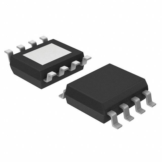
| 描述 | IC REG BUCK ADJ 3A 8SOIC |
| 产品分类 | |
| 品牌 | Allegro MicroSystems, LLC |
| 数据手册 | |
| 产品图片 |
|
| 产品型号 | A8698ELJTR-T |
| PCN过时产品 | |
| PWM类型 | 电流模式 |
| rohs | 无铅 / 符合限制有害物质指令(RoHS)规范要求 |
| 产品系列 | - |
| 产品目录页面 | |
| 供应商器件封装 | 8-SOIC-EP |
| 其它名称 | 620-1177-2 |
| 包装 | 剪切带 (CT) |
| 同步整流器 | 无 |
| 安装类型 | 表面贴装 |
| 封装/外壳 | 8-SOIC(0.154",3.90mm 宽)裸焊盘 |
| 工作温度 | -40°C ~ 85°C |
| 标准包装 | 6,000 |
| 电压-输入 | 8 V ~ 25 V |
| 电压-输出 | 0.8 V ~ 20 V |
| 电流-输出 | 3A |
| 类型 | 降压(降压) |
| 输出数 | 1 |
| 输出类型 | 可调式 |
| 频率-开关 | - |


- 商务部:美国ITC正式对集成电路等产品启动337调查
- 曝三星4nm工艺存在良率问题 高通将骁龙8 Gen1或转产台积电
- 太阳诱电将投资9.5亿元在常州建新厂生产MLCC 预计2023年完工
- 英特尔发布欧洲新工厂建设计划 深化IDM 2.0 战略
- 台积电先进制程称霸业界 有大客户加持明年业绩稳了
- 达到5530亿美元!SIA预计今年全球半导体销售额将创下新高
- 英特尔拟将自动驾驶子公司Mobileye上市 估值或超500亿美元
- 三星加码芯片和SET,合并消费电子和移动部门,撤换高东真等 CEO
- 三星电子宣布重大人事变动 还合并消费电子和移动部门
- 海关总署:前11个月进口集成电路产品价值2.52万亿元 增长14.8%


PDF Datasheet 数据手册内容提取
A8698 Wide Input Voltage 3.0 A Step Down Regulator Features and Benefits Description ▪ 8 to 25 V input range The A8698 is a constant off-time current mode step-down ▪ Integrated DMOS switch regulator with a wide input voltage range. Regulation voltage is ▪ Adjustable fixed off-time set by external resistors, to output voltages as low as 0.8 V. ▪ Highly efficient The A8698 includes an integrated power DMOS switch to ▪ Adjustable 0.8 to 20 V output reduce the total solution footprint. It also features internal compensation, allowing users to design stable regulators with minimal design efforts. The off-time can be set with an external resistor, allowing flexibility in inductor selection. Additionally, the A8698 has a logic level enable pin which can shut the device down and put it into a low quiescent current mode for power sensitive applications. The A8698 is supplied in a low-profile 8-lead SOIC with Package: 8-Lead SOIC with exposed exposed pad (package LJ). Applications include: thermal pad (suffix LJ) ▪ Applications with 8 to 25 V input ▪ Consumer electronics, networking equipment ▪ 12 V lighter-powered applications (portable DVD, etc.) ▪ Point of Sale (POS) applications Approximate Scale 1:1 Typical Application +8 to 24 V Efficiency V = 12.0 V CBOOT IN 0.01 μF CIN3 CIN2 CIN1 92 8325 μVF 8325 μVF 0.22 μF 90 VOUT = 5.0 V BOOT VIN 88 V = 3.3 V 86 OUT %) 84 TESNEBT A8698 VBLIAXS 33L μ1H 3V.O3UVT / 3 A Efficiency ( 887208 VOUT = 2.5 V RTSET R1 76 30.1 k(cid:55) 6.34 k(cid:55) COUT 74 GND FB 330 μF 6.3 V 72 D1 2R 2k(cid:55) ESR 70 0 0.5 1.0 1.5 2.0 2.5 3.0 Load Current (A) Circuit for 12 V step down to 3.3 V at 3 A. Efficiency curves for circuit at left. A8698-DS, Rev. 4
A8698 Wide Input Voltage 3.0 A Step Down Regulator Absolute Maximum Ratings Characteristic Symbol Conditions Min. Typ. Max. Units VIN Supply Voltage V – – 25 V IN VBIAS Input Voltage V –0.3 – 7 V BIAS Switching Voltage V –1 – – V S ENB Input Voltage V –0.3 – 7 V ENB Operating Ambient Temperature Range T Range E –40 – 85 °C A Junction Temperature T(max) – – 150 °C J Storage Temperature T –55 – 150 °C S *Output current rating may be limited by duty cycle, ambient temperature, and heat sinking. Under any set of conditions, do not exceed the specified current ratings, or a junction temperature, T, of 150°C. J Package Thermal Characteristics* R Package θJA PCB (°C/W) LJ 35 4-layer * Additional information is available on the Allegro website. Ordering Information Use the following complete part numbers when ordering: Part Numbera Packingb Description LJ package, SOIC surface mount with A8698ELJTR-T 13 in. reel, 3000 pieces/reel exposed thermal pad aLeadframe plating 100% matte tin. bContact Allegro for additional packing options. Allegro MicroSystems, LLC 2 115 Northeast Cutoff, Box 15036 Worcester, Massachusetts 01615-0036 (508) 853-5000 www.allegromicro.com
A8698 Wide Input Voltage 3.0 A Step Down Regulator Functional Block Diagram BOOT VIN VIN Boot Charge VIN + – LX VOUT L1 D1 ESR COUT ENB Switch PWM Control μC Switch Disable Clamp TSET + – FB – I_Peak I_Demand Error + VBIAS is connected to VOUT COMP Bias Supply when VOUT target is between GND VBIAS 3.3 and 5 V VBB UVLO Soft Start TSD 0.8 V Ramp Generation Allegro MicroSystems, LLC 3 115 Northeast Cutoff, Box 15036 Worcester, Massachusetts 01615-0036 (508) 853-5000 www.allegromicro.com
A8698 Wide Input Voltage 3.0 A Step Down Regulator ELECTRICAL CHARACTERISTICS1,2 at TA = 25°C, VIN = 8 to 25 V (unless noted otherwise) Characteristics Symbol Test Conditions Min. Typ. Max. Units V = LOW, V = 12 V, V = 3.2 V, ENB IN BIAS – 1.0 – mA V = 1.5 V (not switching) FB VIN Quiescent Current I V = LOW, V = 12 V, V < 3 V, VIN(Q) ENB IN BIAS – 4.1 – mA V = 1.5 V FB V = HIGH – – 100 μA ENB VBIAS Input Current I V = V – 3.8 5 mA BIAS BIAS OUT Buck Switch On Resistance R T = 25°C, I = 3 A – 180 – mΩ DS(on) A OUT Fixed Off-Time Proportion Based on calculated value –15 – 15 % Feedback Voltage V 0.784 0.8 0.816 V FB Output Voltage Regulation V I = 0 mA to 3 A –3 – 3 % OUT OUT Feedback Input Bias Current I –400 –100 100 nA FB Soft Start Time t 5 10 15 ms ss V > 0.4 V 3.5 – 5 A FB Buck Switch Current Limit I CL V < 0.4 V – 1.15 – A FB ENB Open Circuit Voltage V Output disabled 2.0 – 7 V OC ENB Input Voltage Threshold V LOW level input (Logic 0), output enabled – – 1.0 V ENB(0) ENB Input Current I V = 0 V –10 – –1 μA ENB(0) ENB VIN Undervoltage Threshold V V rising 6.6 6.9 7.2 V UVLO IN VIN Undervoltage Hysteresis V V falling 0.7 – 1.1 V UVLO(hys) IN Thermal Shutdown Temperature T Temperature increasing – 165 – °C JTSD Thermal Shutdown Hysteresis T Recovery = T – T – 15 – °C JTSD(hys) JTSD JTSD(hys) 1Negative current is defined as coming out of (sourcing) the specified device pin. 2Specifications over the junction temperature range of 0ºC to 125ºC are assured by design and characterization. Allegro MicroSystems, LLC 4 115 Northeast Cutoff, Box 15036 Worcester, Massachusetts 01615-0036 (508) 853-5000 www.allegromicro.com
A8698 Wide Input Voltage 3.0 A Step Down Regulator Performance Characteristics Start-up Operation VOUT; 2.00 V/div. VSW; 10.0 V/div. IOUT; 1.00 A/div. VOUTAC; 500 mV/div. VINAC; 1.00 V/div. IOUT; 2.00 A/div. t t = 10.0 ms/div. t t = 5.00 μs/div. Power Off Transient Response VIN = 12 V, VOUT = 3.3 V VOUTAC; 200 mV/div. VOUT; 2.00 V/div. 1.45 A IOUT; 500 mA/div. IOUT; 1.00 A/div. 1.0 A 1.0 A t t = 1.00 ms/div. t t = 1.00 ms/div. Detail: Step Up Transient Response Detail: Step Down Transient Response VIN = 12 V, VOUT = 3.3 V VIN = 12 V, VOUT = 3.3 V VOUTAC; 500 mV/div. VOUTAC; 500 mV/div. 1.45 A IOUT; 500 mA/div. 1.45 A IOUT; 500 mA/div. 1.0 A 1.0 A t t = 100 μs/div. t t = 100 μs/div. Allegro MicroSystems, LLC 5 115 Northeast Cutoff, Box 15036 Worcester, Massachusetts 01615-0036 (508) 853-5000 www.allegromicro.com
A8698 Wide Input Voltage 3.0 A Step Down Regulator Load Regulation Line Regulation I = 3.0 A OUT 0.2 0.2 0.1 0.1 0 0 %) %) –0.1 Error (–0.1 Error ( –0.2 V OUT–0.2 V OUT –0.3 –0.4 –0.3 –0.5 –0.4 –0.6 0 0.5 1.0 1.5 2.0 2.5 3.0 9 11 13 15 17 19 21 23 25 Load Current (A) VIN (V) Allegro MicroSystems, LLC 6 115 Northeast Cutoff, Box 15036 Worcester, Massachusetts 01615-0036 (508) 853-5000 www.allegromicro.com
A8698 Wide Input Voltage 3.0 A Step Down Regulator Functional Description The A8698 is a fixed off-time, current-mode–controlled buck ON/OFF Control. The ENB pin is externally pulled to ground switching regulator. The regulator requires an external clamping to enable the device and begin the soft start sequence. When the diode, inductor, and filter capacitor, and operates in both continu- ENB is open circuited, the switcher is disabled and the output ous and discontinuous modes. An internal blanking circuit is used decays to 0 V. to filter out transients resulting from the reverse recovery of the Protection. The buck switch will be disabled under one or more external clamp diode. Typical blanking time is 200 ns. of the following fault conditions: The value of a resistor between the TSET pin and ground deter- • V < 6 V IN mines the fixed off-time (see graph in the tOFF section). • ENB pin = open circuit • TSD fault V . The output voltage is adjustable from 0.8 to 20 V, based on OUT the combination of the value of the external resistor divider and When the device comes out of a TSD fault, it will go into a soft start to limit inrush current. the internal 0.8 V ±2% reference. The voltage can be calculated with the following formula: t . The value of a resistor between the TSET pin and ground OFF VOUT = VFB × (1 + R1/R2) (1) determines the fixed off-time. The formula to calculate tOFF (μs) is: Light Load Regulation. To maintain voltage regulation during ⎛1–0.03 V ⎞ light load conditions, the switching regulator enters a cycle-skip- t = R ⎜ BIAS⎟ (2) OFF SET 10.2 × 10⁹ ⎝ ⎠ ping mode. As the output current decreases, there remains some energy that is stored during the power switch minimum on-time. where R (kΩ) is the value of the resistor. Results with the TSET In order to prevent the output voltage from rising, the regulator VBIAS pin connected are shown in the following graph (when skips cycles once it reaches the minimum on-time, effectively VBIAS is not connected, use V = 0 in equation 2): BIAS making the off-time larger. Off-Time Setting versus Resistor Value 200 Soft Start. An internal ramp generator and counter allow the out- 180 put to slowly ramp up. This limits the maximum demand on the 160 external power supply by controlling the inrush current required 140 to charge the external capacitor and any dc load at startup. ) VBIAS = 5 V Ωk 120 Isntatertr,n caullryr,e ntht el irmamit pis i 3s .s5e At t om 1in0i mmus mno.minal rise time. During soft R (TSET 10800 VBIAS = 3.3 V 60 The following conditions are required to trigger a soft start: 40 • V > 6 V 20 IN • ENB pin input falling edge 0 1 2 3 4 5 6 7 8 9 10 11 12 13 14 15 16 • Reset of a TSD (thermal shut down) event t (µs) OFF V . To improve overall system efficiency, the regulator output, BIAS VOUT, is connected to the VBIAS input to supply the operating tON. From the volt-second balance of the inductor, the turn-on bias current during normal operating conditions. During startup time, ton , can be calculated approximately by the equation: the circuitry is run off of the VIN supply. VBIAS should be con- (V +V +I R ) t nected to VOUT when the VOUT target level is between 3.3 and tON = V –IOUT Rf OU–TI L RO–FFV (3) IN OUT DS(on) OUT L OUT 5 V. If the output voltage is less than 3.3 V, then the A8698 can operate with an internal supply and pay a penalty in efficiency, where as the bias current will come from the high voltage supply, VIN. VBIAS can also be supplied with an external voltage source. No V is the voltage drop across the external Schottky diode, f power-up sequencing is required for normal opperation. R is the winding resistance of the inductor, and L Allegro MicroSystems, LLC 7 115 Northeast Cutoff, Box 15036 Worcester, Massachusetts 01615-0036 (508) 853-5000 www.allegromicro.com
A8698 Wide Input Voltage 3.0 A Step Down Regulator R is the on-resistance of the switching MOSFET. to the minimum on-time of the switcher. DS(on) The switching frequency is calculated as follows: The extension of the off-time is based on the value of the TSET 1 multiplier and the FB voltage, as shown in the following table: f = (4) SW t t ON + OFF V (V) TSET Multiplier FB Shorted Load. If the voltage on the FB pin falls below 0.4 V, the < 0.16 8 × t OFF regulator will invoke a 1.5 A typical overcurrent limit to handle < 0.32 4 × t OFF the shorted load condition at the regulator output. For low output < 0.5 2 × t voltages at power up and in the case of a shorted output, the off- OFF > 0.5 t time is extended to prevent loss of control of the current limit due OFF Component Selection L1. The inductor must be rated to handle the total load current. Substituting into equation 8: The value should be chosen to keep the ripple current to a reason- t = 323 mA × 33 μH / 7.95 V = 1.34 μs able value. The ripple current, I , can be calculated by: ON RIPPLE Substituting into equation 7: I = V × t / L (5) RIPPLE L(OFF) OFF f = 1 / (2.67 μs + 1.34 μs) = 250 kHz SW VL(OFF) = VOUT + Vf + IL(AV) × RL (6) Higher inductor values can be chosen to lower the ripple cur- rent. This may be an option if it is required to increase the total maximum current available above that drawn from the switching Example: regulator. The maximum total current available, I , is: LOAD(MAX) Given V = 3.3 V, V = 0.55 V, V = 12 V, I = 3.0 A, OUT f IN LOAD power inductor with L = 33 μH and R = 0.05 Ω Rdc at 55°C, I = I (min) – I / 2 (10) L LOAD(MAX) CL RIPPLE t = 2.67 μs, and R = 0.2 Ω. OFF DS(on) where I (min) is 3.5 A, from the Electrical Chracteristics table. CL Substituting into equation 6: D1. The Schottky catch diode should be rated to handle 1.2 times the maximum load current. The voltage rating should be higher V = 3.3 V + 0.55 V+ 3.0 A × 0.05 Ω = 4.0 V L(OFF) than the maximum input voltage expected during all operating Substituting into equation 5: conditions. The duty cycle for high input voltages can be very close to 100%. I = 4.0 V × 2.67 μs / 33 μH = 323 mA RIPPLE COUT. The main consideration in selecting an output capacitor The switching frequency, f , can then be estimated by: SW is voltage ripple on the output. For electrolytic output capacitors, a low-ESR type is recommended. f = 1 / ( t + t ) (7) SW ON OFF The peak-to-peak output voltage ripple is simply I × ESR. t = I × L / V (8) RIPPLE ON RIPPLE L(ON) Note that increasing the inductor value can decrease the ripple current. The ESR should be in the range from 50 to 500 mΩ. V = V – I × R –I × R – V (9) L(ON) IN L(AV) DS(on) L(AV) L OUT If a low ESR capacitor is used, such as a POSCAP or SP, an extra Substituting into equation 9: R , C circuit is needed to inject ripple into the feedback pin and r r V = 12 V – 3 A × 0.2 Ω – 3 A × 0.05 Ω – 3.3 V = 7.95 V ensure stability. Please refer to the Application Circuit section for L(ON) Allegro MicroSystems, LLC 8 115 Northeast Cutoff, Box 15036 Worcester, Massachusetts 01615-0036 (508) 853-5000 www.allegromicro.com
A8698 Wide Input Voltage 3.0 A Step Down Regulator the connection. The R should be much larger than the feedback Note. The curve represents the minimum RTSET value. When r resistor to prevent any potential offset in output voltage. For calculating R , be sure to use V (max) / V (min). Resistor example, if R < 10 kΩ, R should be 1 MΩ. C should be selected TSET IN OUT f r r based on the following equation: tolerance should also be considered, so that under no operating (V (min) – V ) × t (min) C(max)= IN FB ON (5) conditions the resistance on the TSET pin is allowed to go below r 0.05 × R r the minimum value. where Cr is in pF, t (min) is in μs, and R is in MΩ. ON r FB Resistor Selection. The impedance of the FB network RTSET Selection. Correct selection of RTSET values will ensure that minimum on-time of the switcher is not violated and should be kept low to improve noise immunity. Large value resis- prevent the switcher from cycle skipping. For a given V to IN tors can pick up noise generated by the inductor, which can affect V ratio, the RTSET value must be greater than or equal to the OUT value defined by the curve in the plot below. voltage regulation of the switcher. 13.0 12.5 12.0 11.5 Violation of 11.0 Minimum On-Time 10.5 10.0 99..50 R TSET VOUT88..50 Value of / 7.5 m VIN 7.0 m u 6.5 Mini 6.0 Safe Operating Area 5.5 5.0 4.5 4.0 3.5 3.0 2.5 2.0 10.012.515.017.520.022.525.027.530.032.535.037.540.042.545.047.550.052.555.057.560.062.565.067.570.0 R (k(cid:55)) TSET Allegro MicroSystems, LLC 9 115 Northeast Cutoff, Box 15036 Worcester, Massachusetts 01615-0036 (508) 853-5000 www.allegromicro.com
A8698 Wide Input Voltage 3.0 A Step Down Regulator Application Circuit Efficiency versus Load Current Circuit with Low ESR Capacitor Stabilized with low ESR capacitor fSW = 500 kHz nominal at 12 V 100 90 0C.B0O1OμTF V12IN to 16.4 V %) 8700 BOOT VIN C22INμF 1L0μH V5OVU/T2.5A y ( 60 ENB LX Efficienc 5400 RTSET TSET A8698 VBIAS 1RM3Ω D1 C1128O0UmTμΩF 16.4 kΩ GND FB 30 R1 20 6.34kΩ 100 RLC:aO tCUinDTg:Rs E:HE1F0U4RD-01J0102N1CR 100pF 1R.22kΩ 0 0.5 1.0 1.5 2.0 2.5 3.0 CIN: ECJ-4YB1E226M Load Current (A) Evaluation Board Silkscreen Layer Bottom Layer J1 8 to 24 Vdc C1.2 C1.3 C1.1 J2 GND C3 C2 J4 GND BOOT VIN C4.1 C4.2 J3 R4 A8698 L1 3.3 V / 3.0 A ENB LX D1 C4.3 VOUT TSET VBIAS R3 EN GND FB PAD R2 R1 R5 P1 Top and Silkscreen Layers Allegro MicroSystems, LLC 10 115 Northeast Cutoff, Box 15036 Worcester, Massachusetts 01615-0036 (508) 853-5000 www.allegromicro.com
A8698 Wide Input Voltage 3.0 A Step Down Regulator Evaluation Board Bill of Materials Designator Quantity Description Manufacturer Footprint Part Number C1.1 1 Ceramic chip, 22 μF, 25 V, ±20%, X5R. Panasonic 1210 ECJ4YB1E226M C1.2, C1.3 2 Aluminum electrolytic capacitor, 35 V / 82 μF, 930 Rubycon 35V-ZAV-820-8 X 12 8 mm × 12 mm mA ripple current C2 1 Ceramic capacitor, X7R, ±10%, 0.1 μF / 50 V Murata 0603 GRM188R71H104KA93D C3 1 Ceramic capacitor, X7R, ±10%, 0.01 μF / 50 V Kemet 0603 C0603C103K5RACTU C4.2 0 Special polymer cap, 120 μF / 6.3 V, 15 mΩ Panasonic 7.3 mm × 4.3 mm EEFUD0J121R × 3.1 mm C4.1 0 Ceramic capacitor, X5R, ±20%, 47 μF / 6.3 V Panasonic 1210 ECJ4YB0J476M C4.3 1 Aluminum electrolytic capacitor, 6.3 V / 330 μF, 450 Panasonic EEVFC0J331P 8 mm × 10.2 mm mA ripple current, 300 mΩ L1 1 Inductor, 33 μH, 53 mΩ, 3.9 A, ±20% Sumida 10.3 mm × CDRH127/LDNP-330MC 10.5 mm × 4 mm D1 1 Schottky diode, 40 V / 3.0 A Diodes, Inc. SMA B340 R1 1 Chip resistor, 6.34 kΩ, 1/16 W, 1% Std 0603 Std. R2 3 Chip resistor, 2.0 kΩ,1/16 W, 1% Std 0603 Std. R3 1 Chip resistor, 30.1 kΩ, 1/16 W, 1% Std 0603 Std. R4 1 Chip resistor, 10 kΩ, 1/16 W, 1% Std 0603 Std. R5 1 Chip resistor, 0 Ω, 1/16 W, 1% Std 0603 Std. J1, J2, J3, 4 Header, 2-pin, 100 mil spacing Sullins 0.100 in. × 2 PTC36SAAN J4 P1 1 Test point, Red, 1mm Farnell 0.038 in. 240-345 EN 1 Test point, Black, 1mm Farnell 0.038 in. 240-333 U1 1 Wide Input Voltage Step Down Regulator Allegro ESOIC8 A8698 Allegro MicroSystems, LLC 11 115 Northeast Cutoff, Box 15036 Worcester, Massachusetts 01615-0036 (508) 853-5000 www.allegromicro.com
A8698 Wide Input Voltage 3.0 A Step Down Regulator 6.20 .244 Package LJ 8-Pin SOIC 5.80 .228 0.25 [.010]M B M 5.00 .197 A 8º 8 4.80 .189 0º B 0.25 .010 0.17 .007 4.00 .157 B 3.80 .150 2.41 .095 NOM 1.27 .050 A 0.40 .016 1 2 3.30 .130 0.25 .010 NOM 8X SEATING C SEATING PLANE 0.10 [.004] C PLANE GAUGE PLANE 8X0.51 .020 1.75 .069 0.31 .012 1.35 .053 0.25 [.010]M C A B 0.25 .010 1.27 .050 0.10 .004 0.65 .026 1.27 .050 MAX NOM 1.75 .069 All dimensions reference, not for tooling use NOM (reference JEDEC MS-012 AA) Dimensions in millimeters U.S. Customary dimensions (in.) in brackets, for reference only Dimensions exclusive of mold flash, gate burrs, and dambar protrusions 5.60 .220 Exact case and lead configuration at supplier discretion within limits shown 2.41 .095 NOM A Terminal #1 mark area 2X 0.20 .008 NOM B Exposed thermal pad (bottom surface) MIN C C Reference land pattern layout (reference IPC7351 SOIC127P600X175-9AM); adjust as necessary to meet application process requirements and PCB layout tolerances; when mounting on a multilayer PCB, thermal vias at the exposed thermal pad land can improve thermal dissipation (reference EIA/JEDEC Standard JESD51-5) 1 2 6X 0.20 .008 3.30 .130 MIN NOM Pin-out Diagram Terminal List Table Number Name Description 1 BOOT Gate drive boost node 2 ENB On/off control; logic input BOOT 1 8 VIN 3 TSET Off-time setting ENB 2 7 LX 4 GND Ground Pad TSET 3 6 VBIAS 5 FB Feedback for adjustable regulator 6 VBIAS Bias supply input GND 4 5 FB 7 LX Buck switching node 8 VIN Supply input (Top View) – Pad Exposed pad for enhanced thermal dissipation Allegro MicroSystems, LLC reserves the right to make, from time to time, such de par tures from the detail spec i fi ca tions as may be required to permit improvements in the per for mance, reli- ability, or manufacturability of its products. Before placing an order, the user is cautioned to verify that the information being relied upon is current. Allegro products are not authorized for use as critical components in life-support ap pli anc es, devices, or systems without express written approval. The information included herein is believed to be accurate and reliable. However, Allegro MicroSystems, LLC assumes no re spon si bil i ty for its use; nor for any infringements of pat ents or other rights of third parties that may result from its use. Copyright © 2006-2013 Allegro MicroSystems, LLC Allegro MicroSystems, LLC 12 115 Northeast Cutoff, Box 15036 Worcester, Massachusetts 01615-0036 (508) 853-5000 www.allegromicro.com