ICGOO在线商城 > A8580KLPTR-T

 Datasheet下载
- 型号: A8580KLPTR-T
- 制造商: Allegro
- 库位|库存: xxxx|xxxx
- 要求:
| 数量阶梯 | 香港交货 | 国内含税 |
| +xxxx | $xxxx | ¥xxxx |
查看当月历史价格
查看今年历史价格
A8580KLPTR-T产品简介:
ICGOO电子元器件商城为您提供A8580KLPTR-T由Allegro设计生产,在icgoo商城现货销售,并且可以通过原厂、代理商等渠道进行代购。 提供A8580KLPTR-T价格参考以及AllegroA8580KLPTR-T封装/规格参数等产品信息。 你可以下载A8580KLPTR-T参考资料、Datasheet数据手册功能说明书, 资料中有A8580KLPTR-T详细功能的应用电路图电压和使用方法及教程。
| 参数 | 数值 |
| 产品目录 | 集成电路 (IC) |
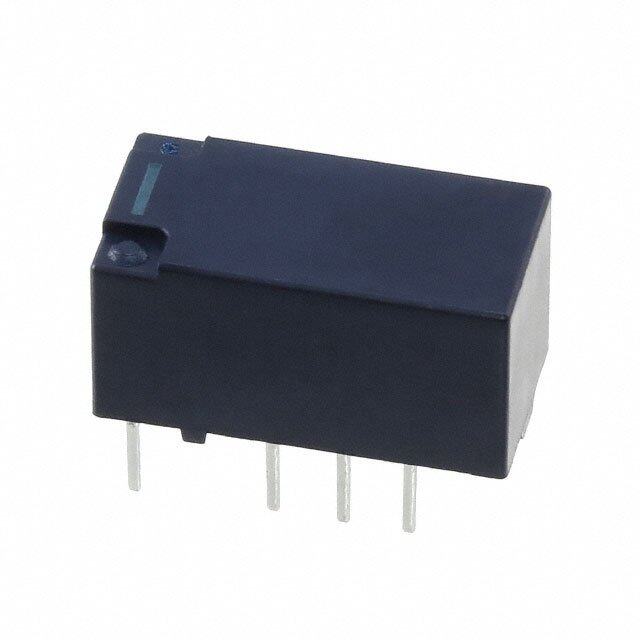
| 描述 | IC REG BUCK ADJ 2.5A 16TSSOP |
| 产品分类 | |
| 品牌 | Allegro MicroSystems, LLC |
| 数据手册 | |
| 产品图片 |
|
| 产品型号 | A8580KLPTR-T |
| PWM类型 | 电流模式 |
| rohs | 无铅 / 符合限制有害物质指令(RoHS)规范要求 |
| 产品系列 | - |
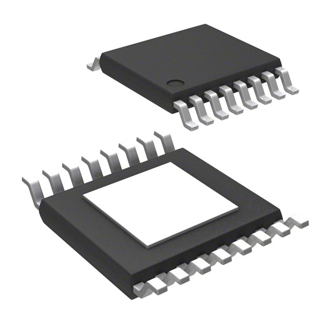
| 供应商器件封装 | 16-TSSOP-EP |
| 其它名称 | 620-1496-6 |
| 包装 | Digi-Reel® |
| 同步整流器 | 无 |
| 安装类型 | 表面贴装 |
| 封装/外壳 | 16-TSSOP (0.173", 4.40mm 宽)裸焊盘 |
| 工作温度 | -40°C ~ 125°C |
| 标准包装 | 1 |
| 特色产品 | http://www.digikey.cn/product-highlights/zh/a8580-regulator/50201 |
| 电压-输入 | 4 V ~ 35 V |
| 电压-输出 | 0.8 V ~ 10 V |
| 电流-输出 | 2.5A |
| 类型 | 降压(降压) |
| 输出数 | 1 |
| 输出类型 | 可调式 |
| 频率-开关 | 250kHz ~ 2.45MHz |


PDF Datasheet 数据手册内容提取
A8580 Wide Input Voltage, 2.4 MHz, 2.5 A, Asynchronous Buck Regulator with Low-IQ Standby, Sleep Mode, External Synchronization, and NPOR Output FEATURES AND BENEFITS DESCRIPTION • Automotive AEC-Q100 qualified Designed to provide the power supply requirements of next • Withstands surge voltages up to 40 V generation car audio and infotainment systems, the A8580 • Operates as low as 3.4 V (typ) with V decreasing provides all the control and protection circuitry to produce a IN IN • Utilizes pulse frequency modulation (PFM) to draw only high current regulator with ±1.0% output voltage accuracy. The tens of microamperes from VIN while maintaining A8580 employs pulse frequency modulation (PFM) to draw keep-alive VOUT less than 50 µA from 12V while supplying 3.3 V/40 µA. IN • PWM/PFMn mode control input pin After startup, the A8580 operates down to at least 3.6 V IN • Delivers up to 2.5 A of output current with integrated (V falling). IN 110 mΩ high voltage MOSFET Features of the A8580 include a PWM/PFMn mode control • SLEEPn input pin commands ultra-low current input to enable PWM (logic high) or PFM (logic low). If shutdown mode the PWM/PFMn input is driven by an external clock signal • Adjustable output voltage with ±1.0% accuracy from 0°C higher than the base frequency ( f ) the PWM frequency to 85°C, ±1.5% from –40°C to 150°C OSC synchronizes to the incoming clock frequency. The SLEEPn • Programmable switching frequency: 250 kHz to 2.4 MHz input pin commands an ultra-low current shutdown mode • Synchronization capability: applying a clock input to the requiring less than 5 µA for internal circuitry and 10 µA (max) PWM/PFMn input pin will increase the PWM frequency for MOSFET leakage at 16 V , 85ºC. The A8580 has external • Active low, power-on reset (NPOR) open-drain output IN compensation to accommodate a wide range of frequencies Continued on the next page… and external components and provides a power-on reset (NPOR) signal validated by the output voltage. Continued on the next page… Package: 16-pin TSSOP with exposed thermal pad (suffix LP) APPLICATIONS: • Automotive: □ Instrument □ Navigation clusters □ HVAC □ Audio Systems Not to scale • Home Audio VIN 1 15 LO 8.2 µH VOUT 2 VIN SW 14 C4.I7N µ1F C4.I7N µ2F C0.I4N73 µF C47IN n4F VIN A8580 SW C47B nOFOT D2 1A/40 V C22O µ1F C22O µ2F C0.O473µF C47O n4F 50 V 50 V 100 V 50 V 5 SMP 16 V X7R 16 V X7R 100 V 50 V 1210 1210 0805 0603 13 GND 16 1210 1210 0805 0603 GND BOOT C15P pF RZ CSS 12389 FCSSSOEMTP BIAS 1101 RFB1147 kΩ CatO 3U.T3 =V 3B8IA.2S µaFnd to 1 04%2.4 t oµleFr taontacle 26.1 kΩ 22 nF VREG FB RFSET C1 CZ 59 kΩ 1 µF RFB2 560 pF 47 kΩ CFB 3.3 V 10 pF RPU EN 4 10 kΩ SLEEPn Mode 6 7 NPOR PWM/PFMn NPOR Typical Application Diagram Typical application schematic, configured for V = 12 V , V = 3.3 V, I = 2.5 A at 425 kHz IN OUT OUT (see Applications Information section for configuration producing V = 5.0 V) OUT A8580-DS, Rev. 9 May 12, 2020 MCO-0000854
Wide Input Voltage, 2.4 MHz, 2.5 A, Asynchronous Buck Regulator A8580 with Low-IQ Standby, Sleep Mode, External Synchronization, and NPOR Output Features and Benefits (continued) Description (continued) • Pre-bias startup capable, VOUT will not cause a reset Extensive protection features of the A8580 include pulse-by-pulse • External compensation for maximum flexibility current limit, hiccup mode short circuit protection, open/short • Stable with ceramic or electrolytic output capacitors asynchronous diode protection, BOOT open/short voltage protection, • Excellent set of protection features to satisfy the most VIN undervoltage lockout, V overvoltage protection and thermal OUT demanding applications shutdown. • Overvoltage, pulse-by-pulse current limit, hiccup mode short The A8580 is supplied in a low profile 16-pin TSSOP package circuit, and thermal protection with exposed power pad (suffix LP). It is lead (Pb) free, with 100% • Robust FMEA, with pin open/short and component faults matte-tin leadframe plating. • Thermally enhanced, surface mount package Selection Guide Operating Ambient Temperature Range Part Number Packing T , (°C) A A8580KLPTR-T –40 to 125 4000 pieces per 13-in. reel Contact Allegro for additional packing options. Table of Contents Specifications 3 Protection Features 19 Absolute Maximum Ratings 3 Undervoltage Lockout (UVLO) 19 Thermal Characteristics 3 Pulse-by-Pulse Overcurrent Protection (OCP) 19 Functional Block Diagram 4 Overcurrent Protection (OCP) and Hiccup Mode 19 Pin-out Diagram and Terminal List 5 BOOT Capacitor Protection 20 Electrical Characteristics 6 Asynchronous Diode Protection 20 Output Overvoltage Protection (OVP) 20 Characteristic Performance 10 Pin-to-Ground and Pin-to-Pin Short Protections 21 Functional Description 12 Thermal Shutdown (TSD) 21 Overview 12 Application Information 25 Reference Voltage 12 Design and Component Selection 25 PWM Switching Frequency 12 Setting the Output Voltage (V ) 25 SLEEPn Input 12 OUT PWM Base Switching Frequency (f R ) 25 PWM/PFMn Input and PWM Synchronization 13 OSC, FSET Output Inductor (L ) 26 BIAS Input Functionality, Ratings, and Connections 13 O Output Capacitors 27 Transconductance Error Amplifier 13 Low-IQ PFM Output Voltage Ripple Calculation 28 Slope Compensation 14 Input Capacitors 28 Current Sense Amplifier 14 Asynchronous Diode (D1) 29 Power MOSFETs 14 Bootstrap Capacitor 29 BOOT Regulator 14 Soft Start and Hiccup Mode Timing (C ) 29 Pulse Width Modulation (PWM) Mode 14 SS Compensation Components (RZ, CZ, and CP) 30 Low-IQ Pulse Frequency Modulation (PFM) Mode 15 A Generalized Tuning Procedure 32 Reduced Current (Low-IP) PWM Mode 17 Power Dissipation and Thermal Calculations 35 Soft Start (Startup) and Inrush Current Control 17 PCB Component Placement and Routing 36 Pre-Biased Startup 18 Typical Applications Schematics 38 Not Power-On Reset (NPOR) Output 18 Package Outline Drawing 39 2 Allegro MicroSystems 955 Perimeter Road Manchester, NH 03103-3353 U.S.A. www.allegromicro.com
Wide Input Voltage, 2.4 MHz, 2.5 A, Asynchronous Buck Regulator A8580 with Low-IQ Standby, Sleep Mode, External Synchronization, and NPOR Output SPECIFICATIONS Absolute Maximum Ratings* Characteristic Symbol Notes Rating Unit VIN, SLEEPn, SS Pin Voltage –0.3 to 40 V Continuous (minimum limit is a function of –0.3 to V + 0.3 V SW Pin Voltage V temperature) IN SW t < 50 ns –1.0 to V + 3 V IN Continuous V – 0.3 to V + 5.5 V SW SW BOOT Pin Voltage V BOOT BOOT OV Fault Condition V – 0.3 to V + 7.0 V SW SW Continuous –0.3 to 5.5 BIAS Pin Voltage V BIAS BIAS OV Fault Condition –0.3 to 6 V All Other Pins Voltage –0.3 to 5.5 V Operating Ambient Temperature T K temperature range –40 to 125 ºC A Maximum Junction Temperature T(max) 150 ºC J Storage Temperature T –55 to 150 ºC stg *Operation at levels beyond the ratings listed in this table may cause permanent damage to the device. The Absolute Maximum ratings are stress ratings only, and func- tional operation of the device at these or any other conditions beyond those indicated in the Electrical Characteristics table is not implied. Exposure to Absolute Maximum- rated conditions for extended periods may affect device reliability. Thermal Characteristics may require derating at maximum conditions, see application information Characteristic Symbol Test Conditions* Value Unit Package Thermal Resistance R On 4-layer PCB based on JEDEC standard 34 ºC/W θJA *Additional thermal information available on the Allegro website. 3 Allegro MicroSystems 955 Perimeter Road Manchester, NH 03103-3353 U.S.A. www.allegromicro.com
Wide Input Voltage, 2.4 MHz, 2.5 A, Asynchronous Buck Regulator A8580 with Low-IQ Standby, Sleep Mode, External Synchronization, and NPOR Output VIN BIAS VREG – REGOV LDO 5.75V + VBIAS rising BOOT REG – 5.0V UVLO O OFF LDOVOUBTIA+S >50mV 33..48VV + BOOFFOT 25O0CmA D Q EN L BOOT VREG BG 1.205V 2V, 4.1V REG – DELAY Digital POR SLEEPn 103µs↓ 2.90V + V4PW00MmOFVFS BOOT BOOT BOOT OFF FAULT + PWM – SE PWM + ISENSE 2x GCSA fSYNC>1.2x fOSC Low IP PWM F CLK FSET fOSC F/2 minOff 110mΩ F/4 S Q sleep V V 750mA R Q Q PWM fSYNC B < 0.2 B < 0.4 PFM CCuormrepnt fSW SW F F DELAY PFM VREG PWM/PFMn 2048↓ Controller 10Ω BOOT > 4.1V DIODEOK FB < 0.8V IFB Error FB Amplifier sPleWeMp CLAMP OCL VREF800mV COMP sleep PWM PslWeeMp – + SS Soft Start 20µA 5µA Offset 400mV FB<700mV (PFM) FB>880mV (PWM) 1kΩ 2kΩ OCL sleep HICCUP HICCUP FAULT PWM LOGIC DIODEOK LOGIC HIC SET BOOT FAULT HIC RST (See Fault REGOV Table) UVLO PULL DOWN POR BOOT OFF TSD NPOR DELAY FB<700mV (PFM) FB>880mV (PWM) 7.5ms↓ FB<740mV (PWM) Functional Block Diagram 4 Allegro MicroSystems 955 Perimeter Road Manchester, NH 03103-3353 U.S.A. www.allegromicro.com
Wide Input Voltage, 2.4 MHz, 2.5 A, Asynchronous Buck Regulator A8580 with Low-IQ Standby, Sleep Mode, External Synchronization, and NPOR Output Pin-out Diagram and Terminal List Table VIN 1 16 BOOT VIN 2 15 SW SS 3 14 SW SLEEPn 4 13 GND PAD GND 5 12 VREG PWM/PFMn 6 11 BIAS NPOR 7 10 FB FSET 8 9 COMP Package LP, 16-pin TSSOP with Exposed Thermal Pad Pin-out Diagram Terminal List Table Name Number Function 11 BIAS Bias input, supplies internal circuitry. High-side gate drive boost input. This pin supplies the drive for the high-side N-channel MOSFET. Connect a 47 nF 16 BOOT ceramic capacitor from BOOT to SW. Output of the error amplifier and compensation node for the current mode control loop. Connect a series RC network from 9 COMP this pin to GND for loop compensation. See the Design and Component Selection section of this datasheet for further details. Feedback (negative) input to the error amplifier. Connect a resistor divider from the regulator output, VOUT, to this pin to 10 FB program the output voltage. Frequency setting pin. A resistor, R , from this pin to GND sets the base PWM switching frequency (f ). See the 8 FSET FSET OSC Design and Component Selection section for information on determining the value of R . FSET 5, 13 GND Ground pins. Active low, power-on reset output signal. This pin is an open drain output that transitions from low to high impedance after 7 NPOR the output has maintained regulation for t . D(NPOR) Exposed pad of the package providing enhanced thermal dissipation. This pad must be connected to the ground plane(s) – PAD of the PCB with at least 6 vias, directly in the pad land. Sets operating output mode (f ). Setting this pin low forces Low-IQ PFM mode (f set by load). Setting this pin high SW SW 6 PWM/PFMn forces PWM mode switching at the the base frequency (f ), set by R . Applying an external clock input to this pin OSC FSET forces synchronization of PWM to the clock input rate (f ), at a rate higher than f . SLEEPn low overrides this pin. SYNC OSC Setting this pin low forces sleep mode (very low current shutdown mode: V = 0 V). This pin must be set high to enable 4 SLEEPn OUT the A8580. If the application does not require a sleep mode, then this pin can be tied directly to VIN. Do not float this pin. Soft start and hiccup pin. Connect a capacitor, C , from this pin to GND to set soft start mode duration. The capacitor 3 SS SS also determines the hiccup period during overcurrent. The source of the high-side N-channel MOSFET. The external free-wheeling diode (D1) and output inductor (L ) should 14, 15 SW O be connected to this pin. Both D1 and L should be placed close to this pin and connected with relatively wide traces. O Power input for the control circuits and the drain of the high-side N-channel MOSFET. Connect this pin to a power supply 1, 2 VIN providing from 4.0 to 35 V. A high quality ceramic capacitor should be placed and grounded very close to this pin. Internal voltage regulator bypass capacitor pin. Connect a 1 µF ceramic capacitor from this pin to ground and place it very 12 VREG close to the A8580. 5 Allegro MicroSystems 955 Perimeter Road Manchester, NH 03103-3353 U.S.A. www.allegromicro.com
Wide Input Voltage, 2.4 MHz, 2.5 A, Asynchronous Buck Regulator A8580 with Low-IQ Standby, Sleep Mode, External Synchronization, and NPOR Output ELECTRICAL CHARACTERISTICS: valid at 4.0 V ≤ V ≤ 35 V, –40°C ≤ T = T ≤ 150°C; unless otherwise specified IN A J Characteristic Symbol Test Conditions Min. Typ. Max. Unit Input Voltage Input Voltage Range1 V 4.0 – 35 V IN VIN UVLO Start V V rising 3.6 3.8 4.0 V INUV(ON) IN VIN UVLO Stop V V falling 3.2 3.4 3.6 V INUV(OFF) IN VIN UVLO Hysteresis V – 400 – mV INUV(HYS) Input Supply Current V ≤ 0.5 V, T = 85°C, V =16 V – 5 15 µA Sleep Mode Input Supply Current2,6 I SLEEPn J IN IN(SLEEP) V ≤ 0.5 V, T = 85°C, V = 35 V – 7 25 µA SLEEPn J IN PWM Mode Input Supply Current2 I V > 3.2 V, I = 0 mA – 2.5 5.0 mA IN(PWM) BIAS OUT V = 12 V, V = 3.3 V, V ≤ 0.8 V, IN OUT PWMPFMn I I = 40 µA, T =25ºC, components selected – – 50 µA LO_IQ(0) OUT A per table 3 V = 12 V, V = 5.0 V, V ≤ 0.8 V, IN OUT PWMPFMn Low-IQ PFM Input Supply Current2,3 I I = 200 µA, T = 25ºC, components selected – – 250 µA LO_IQ(1) OUT A per table 3 V = 12 V, V = 6.5 V, V ≤ 0.8 V, IN OUT PWMPFMn I I = 1 mA, T = 25ºC, components selected – – 750 µA LO_IQ(2) OUT A per table 3 Voltage Regulation 0ºC < T < 85ºC, V ≥ 4.1 V, V = V 792 800 808 mV Feedback Voltage Accuracy4 V J IN FB COMP FB –40ºC < T < 150ºC, V ≥ 4.1 V, V = V 788 800 812 mV J IN FB COMP Low-IQ PFM Mode Output Voltage 3.0 V < V < 5.5 V and I specifications V BIAS LO_IQ 3.3 – 6.5 V Setting Range1,3 OUT(LO_IQ) satisfied PWM Output Voltage Setting Range3 V V = GND, PWM only, no PFM mode 0.8 – 10 V OUT BIAS T = 85°C, DCR ≤ 75 mΩ, V = 3.7 V, A LO IN 3.21 3.3 – V I = 1 A, f = 425 kHz OUT SW T = 85°C, DCR ≤ 75 mΩ, V = 5.6 V, A LO IN 4.96 5.0 – V I = 1 A, f = 425 kHz Output Dropout Voltage3 V OUT SW OUT(SAT) T = 85°C, DCR ≤ 50 mΩ, V = 4.8 V, A LO IN 3.28 3.3 – V I = 1 A, f = 2 MHz OUT SW T = 85°C, DCR ≤ 50 mΩ, V = 7.1 V, A LO IN 4.94 5.0 – V I = 1 A, f = 2 MHz OUT SW 8 V < V < 12 V, components selected per Low-IQ PFM Mode Ripple Voltage3 ΔV IN – 30 65 mV OUT(LO_IQ) table 3 PP Low-IQ PFM Mode Peak Current fSW < 750 kHz – 750 – mAPEAK I Threshold PEAK(LO_IQ) f > 750 kHz – 850 – mA SW PEAK Maximum load to maintain ΔV , Low-IQ PFM Mode DC Load Current3 I OUT(LO_IQ) 400 550 700 mA OUT(LO_IQ) components selected per table 3 Continued on the next page… 6 Allegro MicroSystems 955 Perimeter Road Manchester, NH 03103-3353 U.S.A. www.allegromicro.com
Wide Input Voltage, 2.4 MHz, 2.5 A, Asynchronous Buck Regulator A8580 with Low-IQ Standby, Sleep Mode, External Synchronization, and NPOR Output ELECTRICAL CHARACTERISTICS (continued): valid at 4.0 V ≤ V ≤ 35 V, –40°C ≤ T = T ≤ 150°C; unless otherwise speci- IN A J fied Characteristic Symbol Test Conditions Min. Typ. Max. Unit Error Amplifier Feedback Input Bias Current2 I –38 – –16 nA FB Open Loop Voltage Gain A V = 1.2 V – 65 – dB VOL COMP 400 mV < V 550 750 950 μA/V FB Transconductance g m 0 V < V < 400 mV 275 375 475 μA/V FB Output Current I V = 1.2 V – ±75 – μA EA COMP COMP Pull-Down Resistance R FAULT = 1 or HICCUP = 1 – 1 – KΩ COMP Pulse Width Modulation (PWM) PWM Ramp Offset PWM V level required for 0% duty cycle – 400 – mV OFFS COMP 12 V < V < 16 V, I = 1 A, Minimum Controllable PWM On-Time t IN OUT – 95 135 ns ON(MIN)PWM V – V = 4.5 V BOOT SW Minimum Switch Off-Time t – 95 130 ns OFF(MIN)PWM COMP to SW Current Gain g – 2.85 – A/V mPOWER f = 2.44 MHz 2.1 3.0 3.9 A/μs OSC Slope Compensation3 S f = 1.00 MHz 0.60 0.91 1.2 A/μs E OSC f = 252 kHz 0.14 0.20 0.26 A/μs OSC MOSFET Parameters1 T =25ºC, V – V = 4.5 V, I = 0.4 A – 110 125 mΩ High-Side MOSFET On-Resistance5 R J BOOT SW DS DS(on)HS T =150ºC, V – V = 4.5 V, I = 0.4 A – 190 215 mΩ J BOOT SW DS T < 85°C, V ≤ 0.5 V, V = 0 V, J SLEEPn SW – – 10 µA V = 16 V High-Side MOSFET Leakage2,6 I IN lkg(HS) T ≤ 150°C, V ≤ 0.5 V, V = 0 V, J SLEEPn SW – 60 150 µA V = 16 V IN SW Node Slew Rate3 SR 12 V < V < 16 V – 0.72 – V/ns SW IN Low-Side MOSFET On-Resistance5 R T = 25ºC, V ≥ 6 V, I = 0.1 A – – 10 Ω DS(on)LS J IN DS PWM Switching Frequency R = 8.06 kΩ, V = high 2.20 2.44 2.70 MHz FSET PWM/PFMn Base PWM Switching Frequency f R = 23.7 kΩ, V = high 0.90 1.00 1.10 MHz OSC FSET PWM/PFMn R = 102 kΩ, V = high – 252 – kHz FSET PWM/PFMn PWM Synchronization Timing 1.2 × 1.5 × Synchronization Frequency Range f – − SYNC(MULT) f (typ) f (typ) OSC OSC Synchronized PWM Frequency f – – 2.9 MHz SYNC(PWM) Synchronization Input Duty Cycle D – – 80 % SYNC Synchronization Input Pulse Width t 200 – – ns wSYNC Synchronization Input Rise Time3 t – 10 15 ns rSYNC Synchronization Input Fall Time3 t – 10 15 ns fSYNC Continued on the next page… 7 Allegro MicroSystems 955 Perimeter Road Manchester, NH 03103-3353 U.S.A. www.allegromicro.com
Wide Input Voltage, 2.4 MHz, 2.5 A, Asynchronous Buck Regulator A8580 with Low-IQ Standby, Sleep Mode, External Synchronization, and NPOR Output ELECTRICAL CHARACTERISTICS (continued): valid at 4.0 V ≤ V ≤ 35 V, –40°C ≤ T = T ≤ 150°C; unless otherwise speci- IN A J fied Characteristic Symbol Test Conditions Min. Typ. Max. Unit PWM/PFMn Pin Input Thresholds 3.0 V < V < 3.6 V, V rising – – 2.0 V BIAS PWMPFMn PWM/PFMn High Threshold V PWMPFMn(H) 4.5 V < V < 5.5 V, V rising – – 2.6 V BIAS PWMPFMn 3.0 V < V < 3.6 V, V falling 0.8 – – V BIAS PWMPFMn PWM/PFMn Low Threshold V PWMPFMn(L) 4.5 V < V < 5.5 V, V falling 1.2 – – V BIAS PWMPFMn 3.0 V < V < 3.6 V, V – V – 200 – mV BIAS PWMPFM(H) PWMPFM(L) PWM/PFMn Hysteresis V PWMPFMnhys 4.5 V < V < 5.5 V, V – V – 400 – mV BIAS PWMPFM(H) PWMPFM(L) PWM/PFMn Input Resistance R 120 200 280 kΩ PWMPFMn PWM/PFMn = low, V > HIC/PFM , Low-IQ PFM Transition Delay t SS EN – 2048 – counts D(LO_IQ) NPOR = high PFM Mode Timing f < 1.5 MHz – 435 – ns OSC Constant PFM Off-Time t OFF(PFM) f > 1.5 MHz – 275 – ns OSC Maximum PFM On-Time t – 4.1 – µs ON(PFM)MAX SLEEPn Pin Input Thresholds SLEEPn High Threshold V V rising – 1.3 2.1 V SLEEP(H) SLEEPn SLEEPn Low Threshold V V falling 0.5 1.2 – V SLEEP(L) SLEEPn SLEEPn Delay t V transitioning low 55 103 150 µs D(SLEEP) SLEEPn SLEEPn Input Bias Current I V = 5 V – 500 – nA SLEEPBIAS SLEEPn VREG Pin Output VREG Output Voltage V V = 0 V – 3.05 – V VREG BIAS BIAS Pin Input BIAS Input Voltage Range V 3.2 – 5.5 V BIAS BOOT Regulator BOOT Voltage Enable Threshold V V rising 1.7 2.0 2.2 V BOOT(EN) BOOT BOOT Voltage Enable Hysteresis V – 200 – mV BOOT(HYS) BOOT Voltage Low-Side Switch V V rising – 4.1 – V Disable Threshold BOOTLS(DIS) BOOT Soft Start Pin FAULT, HICCUP Reset Voltage V V falling due to R – 200 275 mV SSRST SS SS(FLT) Hiccup OCP (and Low IQ PFM HIC/PFM V rising – 2.3 – V Counter Enable) Threshold EN SS Maximum Charge Voltage V – V – − SS(MAX) VREG Startup (Source) Current I HICCUP = FAULT = 0 –30 –20 –10 µA SSSU Hiccup (Sink) Current I HICCUP = 1 2.4 5 10 µA SSHIC Pull-Down Resistance R FAULT = 1 or V = low – 2 – kΩ SS(FLT) SLEEPn Continued on the next page… 8 Allegro MicroSystems 955 Perimeter Road Manchester, NH 03103-3353 U.S.A. www.allegromicro.com
Wide Input Voltage, 2.4 MHz, 2.5 A, Asynchronous Buck Regulator A8580 with Low-IQ Standby, Sleep Mode, External Synchronization, and NPOR Output ELECTRICAL CHARACTERISTICS (continued): valid at 4.0 V ≤ V ≤ 35 V, –40°C ≤ T = T ≤ 150°C; unless otherwise speci- IN A J fied Characteristic Symbol Test Conditions Min. Typ. Max. Unit Soft Start Pin (continued) 0 V < V < 200 mV – f / 4 – − FB OSC Soft Start Frequency Foldback f 200 mV < V < 400 mV – f / 2 – − SW(SS) FB OSC 400 mV < V – f – − FB OSC Soft Start Delay Time3 t C = 22 nF – 440 – µs D(SS) SS Soft Start Output Ramp Time3 t C = 22 nF – 880 – µs SS SS Hiccup Modes Hiccup, OCP Count OCP V > 2.3 V and OCL = 1 – 120 – counts LIM SS Hiccup, BOOT Undervoltage BOOT – 120 – counts (Shorted) Count UV Hiccup, BOOT Overvoltage (Open) BOOT – 7 – counts Count OV Overcurrent Protection (OCP) I t = t 3.6 4.1 4.6 A LIM(TONMIN) ON ON(MIN)PWM PWM Pulse-by-Pulse Limit t = (1 / f ) – t , no PWM I ON SW OFF(MIN)PWM 2.3 3.1 3.9 A LIM(TONMAX) synchronization Output Voltage Protection (OVP) VOUT Overvoltage PWM Threshold V V rising, PWM mode 860 880 902 mV OUT(OV)PWM FB VOUT Overvoltage Hysteresis V V falling, relative to V – –10 – mV OUT(OV)HYS FB OUT(OV)PWM VOUT Undervoltage PWM Threshold V V falling, PWM mode 715 740 765 mV OUT(UV)PWM FB VOUT Undervoltage Hysteresis V V rising, relative to V – 10 – mV OUT(UV)HYS FB OUT(UV)PWM VOUT Undervoltage PFM Threshold V V falling, Low-IQ PFM mode 665 700 735 mV OUT(UV)PFM FB Power-On Reset (NPOR) Output NPOR Rising Delay t V rising only 5 7.5 10 ms D(NPOR) FB NPOR Low Output Voltage V I = 5 mA – 185 400 mV NPOR(L) NPOR NPOR Leakage Current2 I V = 5.5 V –1 – 1 µA NPOR(LKG) NPOR Thermal Protection PWM stops immediately and COMP and SS are Thermal Shutdown Rising Threshold3 T 155 170 185 ºC SD pulled low Thermal Shutdown Hysteresis3 T – 20 – ºC SDHYS 1Thermally limited depending on input voltage, output voltage, duty cycle, regulator load currents, PCB layout, and airflow. 2Negative current is defined as coming out of the node or pin, positive current is defined as going into the node or pin. 3Ensured by design and characterization, not production tested. 4Performance at the 0°C and 85°C ranges ensured by design and characterization, not production tested. 5Performance at 25°C ensured by design and characterization, not production tested. 6Performance at 85°C ensured by design and characterization, not production tested. 9 Allegro MicroSystems 955 Perimeter Road Manchester, NH 03103-3353 U.S.A. www.allegromicro.com
Wide Input Voltage, 2.4 MHz, 2.5 A, Asynchronous Buck Regulator A8580 with Low-IQ Standby, Sleep Mode, External Synchronization, and NPOR Output CHARACTERISTIC PERFORMANCE Reference Voltage versus Temperature Switching Frequency versus Temperature 808 3.50 806 fOSC = 2.44 MHz 3.00 fOSC = 1.00 MHz 804 2.50 802 mV) Hz) ( 800 M 2.00 VVREF 798 f (OSC 1.50 796 1.00 794 792 0.50 -50 -25 0 25 50 75 100 125 150 -50 -25 0 25 50 75 100 125 150 Temperature (°C) Temperature (°C) VIN UVLO Start and Stop Thresholds V Overvoltage and Undervoltage Thresholds OUT versus Temperature versus Temperature 3.9 950 3.8 900 ds (V) 3.7 olds (V) 850 O Threshol 3.6 SSTTAORPT, ,V VININUUVV(O(OFNF)) UV Thresh 800 VVVOOOUUUTTT(((UUOVVV)))PPPFWWMMM UVL 3.5 and 750 VIN OV T 3.4 OU 700 V 3.3 650 -50 -25 0 25 50 75 100 125 150 -50 -25 0 25 50 75 100 125 150 Temperature (°C) Temperature (°C) Pulse-by-Pulse Current Limit at t Error Amplifier Transconductance ON(MIN)PWM (ILIM(TONMIN))versus Temperature versus Temperature 4.50 900 VVFFBB>>440000 m mVV 4.40 800 VVFFBB<<440000 mmVV 4.30 V) 700 / A µ A) 4.20 e( 600 ( n MIN) 4.10 ucta 500 N d O n M(T 4.00 sco 400 ILI an 3.90 Tr 300 3.80 200 3.70 100 -50 -25 0 25 50 75 100 125 150 -50 -25 0 25 50 75 100 125 150 Temperature (°C) Temperature (°C) 10 Allegro MicroSystems 955 Perimeter Road Manchester, NH 03103-3353 U.S.A. www.allegromicro.com
Wide Input Voltage, 2.4 MHz, 2.5 A, Asynchronous Buck Regulator A8580 with Low-IQ Standby, Sleep Mode, External Synchronization, and NPOR Output PWM/PFMn High and Low Voltage Thresholds PWM/PFMn High and Low Voltage Thresholds versus Temperature, V = 3.3 V versus Temperature, V = 5.0 V BIAS BIAS 1.60 2.3 VPWMPFMn(H) VPW MPFMn(H) 1.55 VPW MPFMn(L) 2.2 VPW MPFMn(L) V) 1.50 V) ds ( ds ( 2.1 ol 1.45 ol h h hres 1.40 hres 2.0 T T Mn 1.35 Mn 1.9 F F /P 1.30 /P M M 1.8 W W P 1.25 P 1.7 1.20 1.15 1.6 -50 -25 0 25 50 75 100 125 150 -50 -25 0 25 50 75 100 125 150 Temperature (°C) Temperature (°C) SLEEPn High and Low Voltage Thresholds SS Start and Hiccup Currents versus Temperature versus Temperature 1.60 25.0 VSLEEP(H) Startup, ISSSU VSLEEP(L) Hiccup, ISSHIC V) 1.40 20.0 s ( d eshol 1.20 µA)15.0 n Thr ent ( EP 1.00 urr10.0 LE C S 0.80 5.0 0.60 0 -50 -25 0 25 50 75 100 125 150 -50 -25 0 25 50 75 100 125 150 Temperature (°C) Temperature (°C) NPOR Low Output Voltage at 5 mA NPOR Time Delay versus Temperature versus Temperature 400 8.00 7.90 350 7.80 300 7.70 mV) 250 ms) 7.60 V (NPOR 125000 (D(NPOR) 77..4500 t 7.30 100 7.20 50 7.10 0 7.00 -50 -25 0 25 50 75 100 125 150 -50 -25 0 25 50 75 100 125 150 Temperature (°C) Temperature (°C) 11 Allegro MicroSystems 955 Perimeter Road Manchester, NH 03103-3353 U.S.A. www.allegromicro.com
Wide Input Voltage, 2.4 MHz, 2.5 A, Asynchronous Buck Regulator A8580 with Low-IQ Standby, Sleep Mode, External Synchronization, and NPOR Output FUNCTIONAL DESCRIPTION Overview airflow, PCB layout, and PCB construction. Figure 1 shows calculated current ratings versus ambient temperature for V = IN The A8580 is an asynchronous, current mode, buck regulator that 12 V, and V = 3.3 V and 5.0 V, at both f = 425 kHz and OUT SW incorporates all the control and protection circuitry necessary to f = 2 MHz. This analysis assumed a 4-layer PCB constructed SW provide the power supply requirements of car audio and infotain- according to the JEDEC standard (vielding a thermal resistance ment systems. of 34°C/W), with no nearby heat sources, and no airflow. The A8580 has three modes of operation. First, the A8580 can Reference Voltage deliver up to 2.5 A in pulse width modulation (PWM) mode. Second, in Low-IQ pulse frequency modulation (PFM) mode, The A8580 incorporates an internal reference that allows output the A8580 will draw only tens of microamperes from V while voltages ( V ) as low as 0.8 V. The accuracy of the internal IN OUT maintaining V (at no load). Under most conditions, Low-IQ reference is ±1.0% from 0°C to 85°C and ±1.5% from −40°C to OUT PFM mode is typically capable of supporting up to 550 mA. 150°C. The output voltage is programmed by connecting a resis- Third, with the SLEEPn pin low, the A8580 will enter an ultra- tor divider from VOUT to the FB pin of the A8580, as shown in low current shutdown (sleep) mode where V = 0 V and the the Typical Applications schematics. OUT total current drawn from V will typically be less than 10 µA. IN PWM Switching Frequency The PWM/PFMn input pin is used to select either PWM or The PWM switching frequency of the A8580 is adjustable from Low-IQ PFM mode. In PFM mode the A8580 is able to supply a 250 kHz to 2.4 MHz and has an accuracy of about ±10% across relatively high amount of current (typically 550 mA). This allows the operating temperature range. enough current for a microcontroller or DSP to fully power-up. After power-up, to obtain the full current capability of the A8580, During startup, the PWM switching frequency changes from 25% the microcontroller or DSP must change the PWM/PFMn input to 50% and finally to 100% of f , as V rises from 0 V to OSC OUT from a logic low to a logic high to force PWM mode. This will the regulation voltage. The startup switching frequency is dis- provide full current to the remainder of the system. cussed in more detail in the section describing soft start, below. The A8580 was designed to support up to 2.5 A. However, the If the regulator output is shorted to ground, V ≈ 0 V, the PWM FB exact amount of current it will supply, before possible thermal frequency will be 25% of f . In this case, the extra low switch- OSC shutdown, depends heavily on: duty cycle, ambient temperature, ing frequency allows extra off-time between SW pulses. The extra off-time allows the output inductor current to decay back to 0 A before the next SW pulse occurs. This prevents the inductor current from climbing to a value that could damage the A8580 or the output inductor. SLEEPn Input The A8580 has a SLEEPn logic level input pin. To get the A8580 to operate, the SLEEPn pin must be a logic high (>2.1 V). The SLEEPn pin is rated to 40 V, allowing the SLEEPn pin to be con- VIN = 12 V, VOUT = 5 V, fSW = 2 MHz nected directly to VIN if there is no suitable logic signal available VIN = 12 V, VOUT = 5 V, fSW = 425 kHz to wake up the A8580. VIN = 12 V, VOUT = 3.3 V, fSW = 2 MHz When SLEEPn transitions low, the A8580 waits approximately VIN = 12 V, VOUT = 3.3 V, fSW = 425 kHz 103 µs before shutting down. This delay provides plenty of filtering to prevent the A8580 from prematurely entering sleep mode because of any small glitch coupling onto the PCB trace or SLEEPn pin. Figure 1: A8580 Typical Current Derating 12 Allegro MicroSystems 955 Perimeter Road Manchester, NH 03103-3353 U.S.A. www.allegromicro.com
Wide Input Voltage, 2.4 MHz, 2.5 A, Asynchronous Buck Regulator A8580 with Low-IQ Standby, Sleep Mode, External Synchronization, and NPOR Output PWM/PFMn Input and PWM Synchronization tively high voltage and an LDO is very inefficient and generates extra heat. To improve efficiency, especially in Low-IQ PFM The PWM/PFMn pin provides two major functions. It is a control mode, a BIAS pin is utilized. For most applications, the BIAS pin input that sets the operating mode, and also an optional clock should be connected directly to the output of the regulator, V . OUT input for setting PWM frequency. When V rises to an adequate level (approximately 3.1 V), the OUT If PWM/PFMn is a logic high, the A8580 operates in PWM A8580 will shut down the inefficient LDO and begin running its mode. If PWM/PFMn is a logic low, the A8580 operates in control circuitry directly from the output of the regulator. This Low-IQ PFM (keep alive) mode. When PWM/PFMn transitions makes the A8580 much more efficient and cooler. from logic high to logic low, the A8580 checks for V >2.3 V SS The BIAS pin is designed to operate in the range from and NPOR at logic high. If these two conditions are satisfied, 3.2 to 5.5 V. If the output of the regulator is in this range, then then the A8580 will wait 2048 internal clock cycles and then V should be routed directly to the BIAS pin. However, if OUT enter Low-IQ PFM mode. This delay provides plenty of filter- the output of the regulator is above 5.6 V, then a very small ing to prevent the regulator from prematurely entering PFM LDO, capable of at least 5 mA, must be used to reduce the volt- mode because of any small glitch coupling onto the PCB trace or age to either 3.3 V or 5.0 V before routing it to the BIAS pin. PWM/PFMn pin. Operating with an external LDO will reduce the efficiency in Also, note that the SLEEPn pin must be a logic high or the Low-IQ PFM mode. PWM/PFMn input has no effect. The interaction between the The BIAS pin may be driven by an external power supply. For SLEEPn pin and PWM/PFMn pin is summarized in Table 1. startup, there are no sequencing requirements between VIN and If an external clock is applied to the PWM/PFMn pin, the A8580 BIAS. However, for shutdown, VIN should be removed before synchronizes its PWM frequency to the external clock. The BIAS. If BIAS is removed before VIN it will cause the A8580 to external clock may be used to increase the A8580 base PWM reset. The reset will cause the A8580 to terminate PWM switch- frequency (fOSC) set by RFSET. Synchronization operates from ing and VOUT will decay. Also, NPOR, VSS , and VCOMP will be 1.2 × f (typ) to 1.5 × f (typ) . The external clock pulses must pulled low. Ideally, the SLEEPn pin should be used to set the OSC OSC satisfy the pulse width, duty cycle, and rise/fall time requirements mode of the A8580 before VIN and/or BIAS are turned on or off. shown in the Electrical Characteristics table in this datasheet. If the BIAS pin is grounded, the A8580 will simply operate continuously from VIN. However, during PFM mode, the input BIAS Input Functionality, Ratings, and Con- current will increase, and the PFM efficiency will be significantly nections reduced. When the A8580 is powering up, it operates from an internal Transconductance Error Amplifier LDO regulator, directly from VIN. However, V can be a rela- IN The transconductance error amplifier primary function is to con- trol the regulator output voltage. The error amplifier is shown in Table 1: A8580 Modes of Operation Figure 2. Here, it is shown as a three-terminal input device with Pin Inputs Operating Mode two positive and one negative input. The negative input is simply SLEEPn PWM/PFMn Name Description Low Don’t care Sleep V = 0 V OUT High High f = f SW OSC V = OK 400 mV OUT PWM fSW = and High PWM/PFMn IOUT ≤ 2.5 A SS Pin Error Amplifier clock in + Enter Low-IQ PFM after 2048 cycles, High if V > 2.3 V (typ) and NPOR = high + CPiOnMP SS VREF - VOUT = OK 800 mV f is VOUT and High Low Low-IQ PFM SW dependent I ≤ OUT 550 mA (typ) FB Pin High Low Low-IP PWM Fault, I at 50% LIM Figure 2: The A8580 Error Amplifier 13 Allegro MicroSystems 955 Perimeter Road Manchester, NH 03103-3353 U.S.A. www.allegromicro.com
Wide Input Voltage, 2.4 MHz, 2.5 A, Asynchronous Buck Regulator A8580 with Low-IQ Standby, Sleep Mode, External Synchronization, and NPOR Output connected to the FB pin and is used to sense the feedback voltage BOOT Regulator for regulation. The two positive inputs are used for soft start and The A8580 contains a regulator to charge the boot capacitor. steady-state regulation. The error amplifier performs an analog The voltage across the BOOT capacitor is typically 5.0 V. If OR selection between its two positive inputs. The error amplifier the BOOT capacitor is missing, the A8580 detects a boot over- regulates to either the soft start pin voltage (minus 400 mV) or voltage. Similarly, if the BOOT capacitor is shorted the A8580 the A8580 internal reference, V , whichever is lower. REF detects a boot undervoltage. Also, the BOOT regulator has a To stabilize the regulator, a series RC compensation network current limit to protect itself during a short circuit condition. The (RZ and CZ) must be connected from the error amplifier output details of how each type of boot fault is handled by the A8580 are (the COMP pin) to GND, as shown in the Typical Applica- shown in Figures 13 and 14 and summarized in table 2. tions schematics. In most instances an additional, relatively low value, capacitor (CP) should be connected in parallel with the Pulse Width Modulation (PWM) Mode RZ-CZ components to reduce the loop gain at very high frequen- The A8580 utilizes fixed-frequency, peak current mode control to cies. However, if the CP capacitor is too large, the phase mar- provide excellent load and line regulation, fast transient response, gin of the regulator may be reduced. Calculating RZ, CZ, and and ease of compensation. A high-speed comparator and control CP is covered in detail in the Component Selection section of logic, capable of typical pulse widths of 95 ns, are included in the this datasheet. A8580. The inverting input of the PWM comparator is connected If a fault occurs or the regulator is disabled (SLEEPn = low), the to the output of the error amplifier. The non-inverting input is COMP pin is pulled to GND via approximately 1 kΩ and PWM connected to the sum of the current sense signal, the slope com- switching is inhibited. pensation, and a DC offset voltage (V , 400 mV (typ) ). PWMOFFS At the beginning of each PWM cycle, the CLK signal sets the Slope Compensation PWM flip flop and the high-side MOSFET is turned on. When The A8580 incorporates internal slope compensation (SE ) to the summation of the DC offset, slope compensation, and current allow PWM duty cycles above 50% for a wide range of input/out- sense signal rises above the error amplifier voltage, the PWM flip put voltages and inductor values. The slope compensation signal flop is reset and the high-side MOSFET is turned off. is added to the sum of the current sense amplifier output and the The PWM flip flop is reset-dominant, so the error amplifier PWM ramp offset. As shown in the Electrical Characteristics may override the CLK signal in certain situations. For example, table, the amount of slope compensation scales with the base at very light loads or extremely high input voltages the error switching frequency set by R (f ). The amount of slope FSET OSC amplifier reduces (temporarily) output voltage below the 400 mV compensation does not change when the regulator is synchro- DC offset and the PWM flip flop will ignore one or more of the nized to an external clock. incoming CLK pulses. The high-side MOSFET will not turn The value of the output inductor should be chosen such that SE is on, and the regulator will skip pulses to maintain output voltage from 0.5× to 1× the falling slope of the inductor current (SF). regulation. Current Sense Amplifier The A8580 incorporates a high-bandwidth current sense ampli- fier to monitor the current in the high-side MOSFET. This current signal is used by both the PWM and PFM control circuitry to n) o regulate the peak current. The current signal is also used by the S( D R protection circuitry to prevent damage to the A8580. d e z Power MOSFETs ali m or The A8580 includes a 40 V, 110 mΩ high-side N-channel N MOSFET, capable of delivering at least 2.5 A. The A8580 also includes a 10 Ω, low-side MOSFET to help ensure the BOOT capacitor is always charged. The typical R increase versus DS(on) Temperature (°C) temperature is shown in Figure 3. Figure 3: Typical MOSFET R versus Temperature DS(on) 14 Allegro MicroSystems 955 Perimeter Road Manchester, NH 03103-3353 U.S.A. www.allegromicro.com
Wide Input Voltage, 2.4 MHz, 2.5 A, Asynchronous Buck Regulator A8580 with Low-IQ Standby, Sleep Mode, External Synchronization, and NPOR Output In PWM mode all of the A8580 fault detection circuits are active. After the high-side MOSFET is turned off, the A8580 will again See Figure 13 for a timing diagram showing how faults are han- delay approximately t and either: OFF(PFM) dled when in PWM mode. Also, the Protection Features section • turn on the MOSFET again, if V < 800 mV, or of this datasheet provides a detailed description of each fault and FB • return to the Low-IQ PFM mode Table 2 presents a summary. Figures 4 and 5 demonstrate Low-IQ PFM mode operation for a Low-IQ Pulse Frequency Modulation (PFM) light load (66 mA) and a heavy load (330 mA), respectively. Mode In Low-IQ PFM mode the average current drawn from the input supply depends primarily on both the load, and how often the The A8580 enters Low-IQ PFM mode after 2048 internal clock A8580 must fully power-up to maintain regulation. In Low-IQ cycles, if SLEEPn is high, V > HIC/PFM (2.3 V (typ)), and SS EN PFM mode the following faults are detected: a missing asynchro- NPOR is high. In Low-IQ PFM mode, the regulator operates with nous diode, an open or shorted boot capacitor, VOUT shorted a switching frequency, f , that depends on the load condition. SW to ground, and SW shorted to ground. As described in the next In Low-IQ PFM mode, a comparator monitors the voltage at section, if any of these faults occur the A8580 will transition the FB pin. If V is above about 800 mV, the A8580 remains from Low-IQ PFM mode to Low-IP PWM mode, with operation FB in coast mode and draws extremely low current from the input at 50% of the current limit of the PWM switching mode. See supply. Figure 14 for a timing diagram showing operation of the A8580 in Low-IQ PFM mode. If the voltage at the FB pin drops below about 800 mV, the A8580 will fully power-up, delay approximately 2.5 µs while it wakes In Low-IQ PFM mode the A8580 dissipates very little power, so up, and then turn on the high-side MOSFET . V will rise at the thermal monitoring circuit (TSD) is not needed and is dis- OUT a rate dependent on the input voltage, inductor value, output abled to minimize the quiescent current and improve efficiency. capacitance, and load. The high-side MOSFET will be turned off Figure 6 shows PWM to Low-IQ PFM transitions for a typical when either: microcontroller or DSP system. The system starts in PWM mode • current in the high-side MOSFET reaches I , or at I = 250 mA and then transitions to Low-IQ PFM mode, PEAK(LO_IQ) OUT • the high-side MOSFET has been on for t . also at I = 250 mA (time A). While in Low-IQ PFM mode the ON(PFM)MAX OUT VOUT 3.3 V VOUT 3.3 V 18.5 µs tOFF(PFM) = 435 ns VSW VSW IPEAK(LO_IQ) IPEAK(LO_IQ) IL IL Figure 4: Low-IQ PFM Mode Operation at V = 12 V, Figure 5: Low-IQ PFM Mode Operation at V = 12 V, IN IN V = 3.3 V, and I = 66 mA. SW turns on only once V = 3.3 V, and I = 330 mA. SW turns on only OUT OUT OUT OUT every 18.5 µs to regulate V twice every 5 µs to regulate V OUT OUT 15 Allegro MicroSystems 955 Perimeter Road Manchester, NH 03103-3353 U.S.A. www.allegromicro.com
Wide Input Voltage, 2.4 MHz, 2.5 A, Asynchronous Buck Regulator A8580 with Low-IQ Standby, Sleep Mode, External Synchronization, and NPOR Output VOUT B D Overall Waveforms C A E IOUT VPWM/PFMn VOUT VOUT B C A IOUT IOUT VPWM/PFMn VPWM/PFMn Time A: Transition from PWM to PFM at 250 mA Time C: Load steps from 0 A to 100 mA and back to Time B: Load steps from 250 mA to 0 A in Low-IQ PFM 0 A in Low-IQ PFM mode mode VOUT VOUT D IOUT E IOUT VPWM/PFMn VPWM/PFMn Time D: Load steps from 0 A to 250 mA in Low-IQ PFM Time E: Transition from Low-IQ PFM to PWM mode at 250 mode mA Figure 6: Transitions between PWM Mode and Low-IQ PFM Mode, and Load Transient Responses; using circuit in typical application schematic B (V = 12 V, V = 5 V, f = 425 kHz) IN OUT SW 16 Allegro MicroSystems 955 Perimeter Road Manchester, NH 03103-3353 U.S.A. www.allegromicro.com
Wide Input Voltage, 2.4 MHz, 2.5 A, Asynchronous Buck Regulator A8580 with Low-IQ Standby, Sleep Mode, External Synchronization, and NPOR Output current drops from 250 mA to 0 A (time B) and cycles from no to 800 mV, and the regulator output voltage rises from 0 V to the load to 100 mA (time C). In Low-IQ PFM mode the load steps targeted setpoint, which is determined by the feedback resistor from I = 0 A to 250 mA (time D) and then the A8580 transi- divider on the FB pin. OUT tions back to PWM mode (time E). For this example, the output During startup, the PWM switching frequency is reduced to 25% ripple voltage is always less than 30 mV and the transient PP of f while V is below 200 mV. If V is above 200 mV but deflection between modes is always less than 50 mV . OSC FB FB PEAK below 400 mV, the switching frequency is reduced to 50% of Reduced Current (Low-IP) PWM Mode fOSC . Also, if VFB is below 400 mV, the gm of the error amplifier is reduced to g / 2. When V is above 400 mV the switching m FB The A8580 supports two different levels of current limiting in frequency will be f and the error amplifier gain will be g . OSC m PWM modes: The reduced switching frequencies and error amplifier gain are • 100% current, which is during normal PWM, and necessary to help improve output regulation and stability when • Low-IP, in which the current is limited to about 50% of the VOUT is at a very low voltage. When VOUT is very low, the typical current limit PWM control loop requires on-times near the minimum control- The Low-IP PWM mode is invoked when the A8580 is supposed lable on-time, as well as extra-low duty cycles that are not pos- to be in PFM mode but a fault occurs. The purpose of the Low-IP sible at the base operating switching frequencies. PWM mode is to give priority to maintaining reliable regula- When the voltage at the soft start pin reaches approximately tion of V while enabling all the protection circuits inside the OUT 1.2 V, the error amplifier will change mode and begin regulating A8580 that are normally debiased during Low-IQ PFM mode the voltage at the FB pin to the A8580 internal reference, 800 mV. (high precision comparators, timers, and counters). The voltage at the soft start pin will continue to rise to approxi- There are several faults that cause a transition from Low-IQ mately VREG . Complete soft start operation from VOUT = 0 V is PFM to Low-IP PWM mode: a missing asynchronous diode, an shown in Figure 7. open or shorted boot capacitor, VOUT shorted to ground, or SW shorted to ground. See Figure 14 for a timing diagram showing operation when the A8580 transitions from Low-IQ PFM mode to Low-IP PWM mode. VSLEEPn 3.3 V Soft Start (Startup) and Inrush Current Control tD(SS) tSS VSS = 1.2 V Inrush current is controlled by a soft start function. When the A8580 is enabled and all faults are cleared, the soft start pin will source I and the voltage on the soft start capacitor, C , will SSSU SS VOUT ramp upward from 0 V. When the voltage at the soft start pin VSS = 400 mV exceeds approximately 400 mV, the error amplifier will slew its VCOMP output voltage above the PWM Ramp Offset ( V ). At that instant, the high-side and low-side MOSFETs wPiWll MbOeFgFiSn switch- VSS fSW ing. As shown in Figure 7, there is a small delay (tD(SS) ) between IL fSW/4 fSW/2 when the enable pin transitions high, and when both the soft start voltage exceeds 400 mV and the error amplifier slews its output high enough to initiate PWM switching. Figure 7: Normal Startup to V = 3.3 V and I = After the A8580 begins switching, the error amplifier will regu- OUT OUT 1.6 A; PWM/PFMn pin = high, SLEEPn pin transitions late the voltage at the FB pin to the soft start pin voltage minus from low to high approximately 400 mV. During the active portion of soft start, the voltage at the soft start pin rises from 400 mV to 1.2 V (a difference of 800 mV), the voltage at the FB pin rises from 0 V 17 Allegro MicroSystems 955 Perimeter Road Manchester, NH 03103-3353 U.S.A. www.allegromicro.com
Wide Input Voltage, 2.4 MHz, 2.5 A, Asynchronous Buck Regulator A8580 with Low-IQ Standby, Sleep Mode, External Synchronization, and NPOR Output If the A8580 is disabled or a fault occurs, the internal fault latch Not Power-On Reset (NPOR) Output will be set and the capacitor on the soft start pin will be dis- The A8580 has an inverted power-on reset output (NPOR) with a charged to ground very quickly by an internal 2 kΩ pull-down fixed delay of its rising edge ( t ). The NPOR output is an resistor. The A8580 will clear the internal fault latch when the D(NPOR) open drain output so an external pull-up resistor must be used, as voltage at the soft start pin decays to approximately 200 mV shown in the Typical Applications schematics. NPOR transitions (V ). Conversely, if the A8580 enters hiccup mode, the SSRST high when the output voltage ( V ), sensed at the FB pin, is capacitor on the soft start pin is slowly discharged by a current OUT within regulation. In PWM mode, NPOR is high when the output sink, I . Therefore, the soft start capacitor (C ) not only SSHIC SS voltage is typically within 92.5% to 110% of the target value. In controls the startup time but also the time between soft start PFM mode, NPOR is high when the output voltage is typically attempts in hiccup mode. Hiccup mode operation is discussed in above 87.5% of the target value. The NPOR overvoltage and more detail in the Protection Features section of this datasheet. undervoltage comparators incorporate a small amount of hyster- Pre-Biased Startup esis (10 mV typically) and filtering (5 µs typically) to help reduce chattering due to voltage ripple at the FB pin. If the output of the regulator (V ) is pre-biased to some volt- OUT The NPOR output is immediately pulled low either: if an output age, the A8580 will modify the normal startup routine to prevent overvoltage or an undervoltage condition occurs, or if the A8580 discharging the output capacitors. As described previously, the junction temperature exceeds the thermal shutdown threshold error amplifier usually becomes active when the voltage at the (T ). For other faults, NPOR behavior depends on the output soft start pin exceeds 400 mV. If the output is pre-biased, the SD voltage. Table 2 summarizes all the A8580 fault modes and their FB pin will be at some non-zero voltage. The A8580 will not effect on NPOR. start switching until the voltage at the soft start pin increases to approximately V + 400 mV. When the soft start pin volt- At power-up, NPOR must be initialized (set to a logic low) when FB age exceeds this value: the error amplifier becomes active, the V is relatively low. Figure 9 shows V ramping up and NPOR IN IN voltage at the COMP pin rises, PWM switching starts, and V being set to a logic low when V is only 2.2 V. For this test, OUT IN ramps upward from the pre-bias level. Figure 8 shows startup NPOR was pulled up to an external 3.3 V supply via a 2 kΩ resis- when the output voltage is pre-biased to 1.6 V. tor. VSLEEPn VOUT rises from 1.6 V, it is not pulled to 0 V 3.3 V VOUT 1.6 V VSS = 1.2 V VIN = 2.2 V Switching delayed until VSS = VFB +400 mV VIN VSS = 400 mV VNPOR VCOMP VSS fSW IL fSW/2 Figure 8: Pre-biased Startup from V = 1.6 V to V Figure 9: Initialization of NPOR as V Ramps Up OUT OUT IN = 3.3 V, at I = 1.6 A OUT 18 Allegro MicroSystems 955 Perimeter Road Manchester, NH 03103-3353 U.S.A. www.allegromicro.com
Wide Input Voltage, 2.4 MHz, 2.5 A, Asynchronous Buck Regulator A8580 with Low-IQ Standby, Sleep Mode, External Synchronization, and NPOR Output At power-down, NPOR must be held in the logic low state as Because of the addition of the slope compensation ramp to the long as possible. Figure 10 shows V ramping down and NPOR inductor current, the A8580 delivers more current at lower duty IN being held low until V is only 1.3 V. For this test, NPOR was cycles and less current at higher duty cycles. Also, the slope IN pulled up to an external 3.3 V supply via a 2 kΩ resistor. compensation is not a perfectly linear function of switching frequency. For a given duty cycle, this results in a little more cur- Protection Features rent being available at lower switching frequencies than higher frequencies. Figure 11 shows the typical and worst-case min/max The A8580 was designed to satisfy the most demanding automo- pulse-by-pulse current limits versus duty cycle at f = 250 kHz tive and non-automotive applications. In this section, a descrip- SW and 2.45 MHz. tion of each protection feature is described and Table 2 summa- rizes the protection features and operation. If the synchronization input (PWM/PFMn) is used to increase the switching frequency, the on-time and the current ripple will UNDERVOLTAGE LOCKOUT (UVLO) decrease. This will allow slightly more current than at the base switching frequency ( f ). An undervoltage lockout (UVLO) comparator monitors the volt- OSC age at the VIN pin and keeps the regulator disabled if the voltage The exact current the buck regulators can support is heavily is below the stop threshold ( VINUV(OFF) ). The UVLO comparator dependent on: duty cycle ( VIN, VOUT , Vf ), ambient temperature, incorporates some hysteresis ( VINUV(HYS) ) to help reduce on-off thermal resistance of the PCB, airflow, component selection, and cycling of the regulator due to resistive or inductive drops in the nearby heat sources. V path during heavy loading or during startup. IN OVERCURRENT PROTECTION (OCP) AND HICCUP PULSE-BY-PULSE OVERCURRENT PROTECTION MODE (OCP) An OCP counter and hiccup mode circuit protect the buck regula- The A8580 monitors the current in the high-side MOSFET and tor when the output of the regulator is shorted to ground or when if the current exceeds the pulse-by-pulse overcurrent threshold the load is too high. When the voltage at the soft start pin is ( I ) then the high-side MOSFET is turned off. Normal PWM below the hiccup OCP threshold ( HIC/PFM ) the hiccup mode LIM EN operation resumes on the next clock pulse from the internal counter is disabled. Two conditions must be met for the OCP oscillator. The A8580 includes leading edge blanking to prevent counter to be enabled and begin counting: falsely triggering the pulse-by-pulse current limit when the high- • V > HIC/PFM (2.3 V (typ)) and SS EN side MOSFET is turned on. • V is clamped at its maximum voltage (OCL =1) COMP 4.6 4.4 4.2 VIN = 1.3 V VIN 4.0 3.8 3.6 A) (M3.4 ILI VNPOR 3.2 3.0 MMiinn.. aatt 22..4455 MMHHzz 2.8 TTyypp .a at t2 2.4.455 M MHHzz 2.6 MMAaxX._ a2t. 425.4 M5 HMzHz MMIiNn._ a2t5 205 k0H kzHz 2.4 TTYyPp._ a2t5 205 k0H kzHz MMAaxX._ a2t5 205 k0H kzHz 2.2 0 5 10 15 20 25 30 35 40 45 50 55 60 65 70 75 80 85 90 95100 Duty Cycle (%) Figure 10: NPOR being Held Low as V Ramps Down Figure 11: Pulse-by-Pulse Current Limiting versus IN Duty Cycle; at f = 250 kHz (dashed curves) and f = SW SW 2.45 MHz (solid curves) 19 Allegro MicroSystems 955 Perimeter Road Manchester, NH 03103-3353 U.S.A. www.allegromicro.com
Wide Input Voltage, 2.4 MHz, 2.5 A, Asynchronous Buck Regulator A8580 with Low-IQ Standby, Sleep Mode, External Synchronization, and NPOR Output As long as these two conditions are met, the OCP counter BOOT CAPACITOR PROTECTION remains enabled and will count pulses from the overcurrent com- The A8580 monitors the voltage across the BOOT capacitor to parator. If the COMP pin voltage decreases ( OCL = 0 ) the OCP detect if the capacitor is missing or short circuited. If the BOOT counter is cleared. capacitor is missing, the regulator will enter hiccup mode after If the OCP counter reaches OCP counts (120), a hiccup latch 7 PWM cycles. If the BOOT capacitor is short circuited, the LIM is set and the COMP pin is quickly pulled down by a relatively regulator will enter hiccup mode after 120 PWM cycles, provided low resistance (1 kΩ). The hiccup latch also enables a small cur- there is no VOUT overvoltage detection. At no load or very light rent sink connected to the soft start pin ( I ). This causes the loads, the boot charging circuit will increase the output voltage SSHIC voltage at the soft start pin to slowly ramp downward. When the (via the output inductor) and cause an overvoltage condition to be voltage at the soft start pin decays to a low enough level (V , detected if V > V + 5.7 V. SSRST IN OUT 200 mV (typ)) the hiccup latch is cleared and the small current For a boot fault, hiccup mode will operate virtually the same sink turned off. At that instant, the soft start pin will begin to as described previously for an output short circuit fault (OCP) source current ( I ) and the voltage at the soft start pin will SSSU with the soft start pin ramping up and down as a timer to initiate ramp upward. This marks the beginning of a new, normal soft repeated soft start attempts. Boot faults are a non-latched condi- start cycle as described earlier. (Note: OCP is the only fault that tion, so the A8580 will automatically recover when the fault is results in hiccup mode that is ignored when V < 2.3 V.) SS corrected. When the voltage at the soft start pin exceeds the soft start offset (typically 400 mV) the error amplifier forces the voltage ASYNCHRONOUS DIODE PROTECTION at the COMP pin to quickly slew upward and PWM switching If the asynchronous diode (D1 in the Typical Applications sche- will resume. If the short circuit at the regulator output remains, matics) is missing or damaged (open) the SW pin will be subject another hiccup cycle will occur. Hiccups will repeat until the to unusually high negative voltages. These negative voltages may short circuit is removed or the regulator is disabled. If the short cause the A8580 to malfunction and could lead to damage. circuit is removed, the A8580 will soft start normally and the The A8580 includes protection circuitry to detect when the output voltage will automatically recover to the target level, as asynchronous diode is missing. If the SW pin is below typically shown in Figure 12. −1.25 V for more than about 50 ns , the A8580 will enter hic- cup mode after detecting one missing diode fault. Also, if the asynchronous diode is short circuited, the A8580 will experi- ence extremely high currents in the high-side MOSFET. If this occurs the A8580 will enter hiccup mode after detecting one VOUT Short removed short-circuited diode fault. VCOMP 120 OCP counts OUTPUT OVERVOLTAGE PROTECTION (OVP) The A8580 provides a basic level of overvoltage protection by VSS 2.3 V monitoring the voltage level at the FB pin. Two overvoltage con- ditions can be detected: • The FB pin is disconnected from its feedback resistor divider. IL ILIM(TONMIN) 200 mV In this case, a tiny internal current source forces the voltage at the FB pin to rise. When the voltage at the FB pin exceeds the overvoltage threshold ( V , 880 mV (typ)) PWM OUT(OV)PWM switching will stop and NPOR will be pulled low. • A higher, external voltage supply is accidently shorted to the A8580s output. V will probably rise above the overvoltage FB threshold and be detected as an overvoltage condition. In Figure 12. Hiccup Mode Operation and Recovery to this case, the low-side MOSFET will continue to operate V = 3.3 V, I = 1.6 A OUT OUT 20 Allegro MicroSystems 955 Perimeter Road Manchester, NH 03103-3353 U.S.A. www.allegromicro.com
Wide Input Voltage, 2.4 MHz, 2.5 A, Asynchronous Buck Regulator A8580 with Low-IQ Standby, Sleep Mode, External Synchronization, and NPOR Output and can correct the OVP condition, provided that only a few example, logic pins and high voltage pins are separated as much milliamperes of pull-down current are required. In either as possible. Inevitably, some low voltage pins are located adja- case, if the condition causing the overvoltage is corrected the cent to high voltage pins, but in these instances the low voltage regulator will automatically recover. pins are designed to withstand increased voltages, with clamps and/or series input resistance, to prevent damage to the A8580. PIN-TO-GROUND AND PIN-TO-PIN SHORT PROTEC- TIONS THERMAL SHUTDOWN (TSD) The A8580 is designed to satisfy the most demanding automotive The A8580 monitors junction temperature and will stop PWM applications. For example, the A8580 has been carefully designed switching and pull NPOR low if it becomes too hot. Also, to pre- from the very beginning to withstand a short circuit to ground at pare for a restart, the soft start and COMP pins will be pulled low each pin without suffering damage. until V < V . TSD is a non-latched fault, so the A8580 SS SS(RST) In addition, care was taken when defining the A8580 pin-out to will automatically recover if the junction temperature decreases optimize protection against pin-to-pin adjacent short circuits. For by approximately 20°C. 21 Allegro MicroSystems 955 Perimeter Road Manchester, NH 03103-3353 U.S.A. www.allegromicro.com
Wide Input Voltage, 2.4 MHz, 2.5 A, Asynchronous Buck Regulator A8580 with Low-IQ Standby, Sleep Mode, External Synchronization, and NPOR Output TABLE 2: Summary of A8580 Fault Modes and Operation During fault counting, Fault before Hiccup mode BOOT NPOR Reset V Latched? Mode SS High-Side Low-Side Charging State Condition V COMP MOSFET MOSFET Clamped for f / 4 due to Can be Output Hiccup, after OSC Automatic, I , then V < 200 mV, activated if Depends on overcurrent, 120 OCP LIM FB Not affected No after remove pulled low for responds to V is too V V < 200 mV faults BOOT OUT the short FB hiccup V low COMP Clamped for f due to Can be Output Hiccup, after OSC Automatic, I , then V > 400 mV, activated if Depends on overcurrent, 120 OCP LIM FB Not affected No after decrease pulled low for responds to V is too V V > 400 mV faults BOOT OUT load current FB hiccup V low COMP Forced Boot capacitor Hiccup, after Forced off Off after Automatic, Pulled low for off when Depends on open/missing 7 BOOT when BOOT BOOT fault No after replace OV hiccup BOOT fault V (BOOT ) faults OV fault occurs occurs OUT capacitor OV occurs Forced Boot capacitor Hiccup, after Not affected, Forced off Automatic, off when Off only during Depends on shorted 120 BOOT pulled low for only during No after unshort UV BOOT fault hiccup V (BOOT ) faults hiccup UV hiccup OUT capacitor UV occurs Can be Automatic, Asynchronous Hiccup after Pulled low for Forced off activated if Depends on Not affected No after install diode missing 1 fault hiccup after 1 fault V is too V BOOT OUT diode low Asynchronous Can be Automatic, diode (or SW) Hiccup after Pulled low for Forced off activated if Depends on Not affected No after remove hard short to 1 fault hiccup after 1 fault V is too V BOOT OUT short ground low Asynchronous Clamped for Can be Hiccup, after Active, Automatic, diode (or SW) I , then activated if Depends on 120 OCP LIM responds to Not affected No after remove soft short to pulled low for V is too V faults V BOOT OUT short ground hiccup COMP low FB pin open Begins to Transitions Pulled low Automatic, Forced off by Active during Off when V (FB floats ramp up for low via loop FB when V is No after connect low V t is too high FB high) soft start response COMP OFF(MIN)PWM too high FB pin Output Automatic, Transitions Pulled low overvoltage Forced off by Active during Off when V after V Not affected low via loop FB when V is No FB (V > low V t is too high FB returns to FB response COMP OFF(MIN)PWM too high 880 mV) normal range Can be Automatic, Transitions Active, Pulled low Output activated if after V Not affected high via loop responds to Not affected when V is No FB undervoltage V is too FB returns to response V BOOT too low COMP low normal range Pulled low and Pulled low and Automatic, Thermal Forced off by latched until latched until Disabled Off Pulled low No after part shutdown low V V < V V < V COMP cools down SS SSRST SS SSRST VREG Automatic, Transitions or BIAS Forced off by Active during VREG or Not affected low via loop Off Pulled low No overvoltage low V t BIAS to response COMP OFF(MIN)PWM (REGOV) normal range 22 Allegro MicroSystems 955 Perimeter Road Manchester, NH 03103-3353 U.S.A. www.allegromicro.com
Wide Input Voltage, 2.4 MHz, 2.5 A, Asynchronous Buck Regulator A8580 with Low-IQ Standby, Sleep Mode, External Synchronization, and NPOR Output Figure 13: Operation with SLEEPn = high and PWM/PFMn = high (PWM mode) 23 Allegro MicroSystems 955 Perimeter Road Manchester, NH 03103-3353 U.S.A. www.allegromicro.com
Wide Input Voltage, 2.4 MHz, 2.5 A, Asynchronous Buck Regulator A8580 with Low-IQ Standby, Sleep Mode, External Synchronization, and NPOR Output LOW-IP PWM HIHIPWMLO_IQSSSSSSCC 2048 7.5ms Note: Faster SS shown here, so NPOR↑ starts the 2048 PFM delay counter, instead of VSS x1x1 F/4SWF/4F/4thenFFSWSWSWSW/2FSW SS>2.3V •FB>0.74V TOFROMTOFROM2.3V2.3V2.3V2.3V ~500mV LO_IQHICCUP DIODE or SWFAULTS x1 ~500mV 2048 7.5ms FSW SS>2.3V •FB>0.74V SS F/4SWthen/2FSW LOW-IP PWM SHICCSHICCSUPSUP x7 OVx7 OVx120 UVx120 UV F/4F/4SWSW TOFROMTOFROM2.3V2.3V2.3V2.3V HICCUP BOOTFAULTS x7 OVx120 UV LO_IQ ~500mV 2048 7.5ms FSW SS>2.3V •FB>0.74V SS F/4SWthen/2FSW HICCUP M LOW-IP PW OC x120 F/4SW PWM SSLO_IQSSOCHICCUP Vout shorted to GND2048 Note: NPOR=1 already, so V>HIC/PFMSSENstarts the 2048 PFM delay counter 7.5ms x120 F/4SWF/4thenFSWSW/2FSW SS>2.3V •FB>0.74V ~500mV OFF MODE SLEEPn PWM/PFMn TSD NPOR OCHIC_EN HICCUP OCFAULT BOOTFAULT DIODEFAULT VIN SW VOUT SS COMP Figure 14: Operation with SLEEPn = high and PWM/PFMn = low (Low-IQ PFM mode and transition to Low-IP PWM mode) 24 Allegro MicroSystems 955 Perimeter Road Manchester, NH 03103-3353 U.S.A. www.allegromicro.com
Wide Input Voltage, 2.4 MHz, 2.5 A, Asynchronous Buck Regulator A8580 with Low-IQ Standby, Sleep Mode, External Synchronization, and NPOR Output APPLICATION INFORMATION Design and Component Selection SETTING THE OUTPUT VOLTAGE (V ) OUT The output voltage of the regulator is determined by connecting RFB1 a resistor divider from the output node (VOUT) to the FB pin V FB PIN OUT as shown in Figure 15. There are trade-offs when choosing the value of the feedback resistors. If the series combination (RFB1 RFB2 + RFB2) is too low, then the light load efficiency of the regula- tor will be reduced. So, to maximize the efficiency, it is best to choose higher values of resistors. On the other hand, if the paral- lel combination (RFB1 // RFB2) is too high, then the regulator may be susceptible to noise coupling onto the FB pin. Figure 15: Connecting a Feedback Resistor Divider to The feedback resistors must satisfy the ratio shown in the follow- Set the Output Voltage ing equation to produce the target output voltage, V : OUT CFB R V FB1 OUT = – 1 R 0.8 (V) (1) FB2 RFB1 Compared to typical buck regulators, a PFM capable buck VOUT FB PIN regulator presents some unique challenges when determining its feedback divider. This resistor divider must draw minimal current RFB2 C STRAY from VOUT or it will reduce the efficiency during Low-IQ PFM 15 to 25 pF operation. Allegro recommends the resistor values show in Table 3 on page 34. For Low-IQ PFM mode, a feedforward capacitor (CFB) should be connected in parallel with RFB1, as shown in Figure 16. Figure 16: Addition of CFB to Cancel Stray Capacitance The purpose of this capacitor is to offset any stray capacitance at the FB Pin in PFM Mode (C ) from the FB pin to ground. Without CFB, the stray STRAY capacitance and the relatively high resistor values used for the 2.50 feedback network form a low-pass filter and introduce lag to the 2.25 Low-IQ PFM feedback path. The feedforward capacitor helps to 2.00 maintain sensitivity during Low-IQ PFM mode and to assure the 1.75 output voltage ripple is minimized. Hz) 1.50 In general, CFB should be calculated as: M y ( 1.25 c n C > (1.5 × C ) × ( R / R ) (2) ue 1.00 FB STRAY FB2 FB1 q where C is typically 15 to 25 pF. Fre 0.75 STRAY 0.50 PWM BASE SWITCHING FREQUENCY (F R ) 0.25 OSC, FSET The PWM base switching frequency, f , is set by connecting a 0.00 OSC 5.0 15.0 25.0 35.0 45.0 55.0 65.0 75.0 85.0 95.0 resistor from the FSET pin to ground. Figure 17 is a graph show- ing the relationship between the typical switching frequency and RFSET(kΩ) the FSET resistor. The base frequency is the output frequency, Figure 17: PWM Switching Frequency versus R FSET 25 Allegro MicroSystems 955 Perimeter Road Manchester, NH 03103-3353 U.S.A. www.allegromicro.com
Wide Input Voltage, 2.4 MHz, 2.5 A, Asynchronous Buck Regulator A8580 with Low-IQ Standby, Sleep Mode, External Synchronization, and NPOR Output f , when PWMPFMn is high (no external clocking signal). For it is important to calculate an inductor value such that the falling SW a given base switching frequency ( f ), the FSET resistor can slope of the inductor current (S ) will work well with the A8580 OSC F be calculated as follows: slope compensation. The following equation can be used to cal- culate a range of values for the output inductor based on the well- 26385 known approach of providing slope compensation that matches R = – 2.75 FSET f (3) 50% to 100% of the falling slope of the inductor current: OSC V + V V + V where f is in kHz and R is in kΩ. OUT f OUT f OSC FSET ≤ L ≤ 2 × S O S (6) E E When the PWM base switching frequency is chosen the designer should be aware of the minimum controllable on-time, where V is the forward voltage of the asynchronous diode, and t of the A8580. If the system required on-time is less f ON(MIN)PWM L is in µH. than the A8580 minimum controllable on-time, switch node jitter O occurs and the output voltage will have increased ripple or oscil- In equation 6, the slope compensation (S ) is a function of E lations. switching frequency according the following: The PWM base switching frequency required should be calcu- S =0.23 × f 2 + 0.63 × f + 0.038 (7) lated as follows: E OSC OSC VOUT where SE is in A/µs and fOSC is in MHz. f < OSC t × V (4) More recently, Dr. Raymond Ridley presented a formula to calcu- ON(MIN)PWM IN(MAX)REQ late the amount of slope compensation required to critically damp where the double poles at half the PWM switching frequency: V is the output voltage, OUT V +V L ≥ OUT f 1– 0.18 t is the minimum controllable on-time of the A8580 O S D ON(MIN)PWM E (95 ns (typ), 135 ns (max)), and V +V (V (min)+V) V is the maximum required operational input voltage = OUT f 1– 0.18 × IN f IN(MAX)REQ S V +V (8) (not the peak surge voltage). E OUT f If the A8580 PWM synchronization function is employed, then the base switching frequency should be chosen such that jitter This formula allows the inclusion of the duty cycle (D), which will not result at the maximum synchronized switching fre- should be calculated at the minimum input voltage to ensure quency, determined from equation 4: optimal stability. Also, to avoid dropout (that is, saturation of the buck regulator), V (min) must be approximately 1to 1.5 V IN above V when calculating the inductor value with equation 8. V OUT OUT f < 0.66× (5) OSC t × V If equations 7 or 8 yield an inductor value that is not a standard ON(MIN)PWM IN(MAX)REQ value, then the next highest available value should be used. The OUTPUT INDUCTOR (L ) final inductor value should allow for 10% to 20% of initial toler- O ance and 20% to 30% of inductor saturation. For a peak current mode regulator, it is common knowledge that, without adequate slope compensation, the system will become The saturation current of the inductor should be higher than the unstable when the duty cycle is near or above 50%. However, the peak current capability of the A8580. Ideally, for output short cir- slope compensation in the A8580 is a fixed value (S ). Therefore, cuit conditions, the inductor should not saturate even at the high- E 26 Allegro MicroSystems 955 Perimeter Road Manchester, NH 03103-3353 U.S.A. www.allegromicro.com
Wide Input Voltage, 2.4 MHz, 2.5 A, Asynchronous Buck Regulator A8580 with Low-IQ Standby, Sleep Mode, External Synchronization, and NPOR Output est pulse-by-pulse current limit at minimum duty cycle, 4.6 A. The type of output capacitors will determine which terms of This may be too costly. At the very least, the inductor should not equation 11 are dominant. For ceramic output capacitors the ESR- saturate at the peak operating current according to the following: and ESL are virtually zero, so the output voltage ripple COUT COUT will be dominated by the third term of equation 11: S × (V +V ) (9) IPEAK =4.1 – E OUT f ∆V = ∆IL 1.15 × fOSC × (VIN(max)+Vf ) OUT 8 fSWCOUT (12) To reduce the voltage ripple of a design using ceramic output where V (max) is the maximum continuous input voltage, such IN capacitors, simply: increase the total capacitance, reduce the as 18 V (not a surge voltage, such as 40 V). inductor current ripple (that is, increase the inductor value), or Starting with equation 9, and subtracting half of the inductor increase the switching frequency. ripple current, provides us with an interesting equation to predict For electrolytic output capacitors the value of capacitance will the typical DC load capability of the regulator at a given duty be relatively high, so the third term in equation 11 will be very cycle (D): small. The output voltage ripple will be determined primarily by the first two terms of equation 11: S × D V × (1– D) I =4.1 – E OUT (10) OUT(DC) fOSC 2 × fOSC × LO ∆VOUT = ∆IL × ESRCOUT (13) V –V + IN OUT × ESL COUT After an inductor is chosen, it should be tested during output LO short circuit conditions. The inductor current should be monitored To reduce the voltage ripple of a design using electrolytic output using a current probe. A good design would ensure neither the capacitors, simply: decrease the equivalent ESR and ESL inductor nor the regulator are damaged when the output is shorted CO CO by using a high(er) quality capacitor, or add more capacitors in to ground at maximum input voltage and the highest expected parallel, or reduce the inductor current ripple (that is, increase the ambient temperature. inductor value). OUTPUT CAPACITORS The ESR of some electrolytic capacitors can be quite high so The output capacitors filter the output voltage to provide an Allegro recommends choosing a quality capacitor for which the acceptable level of ripple voltage and they store energy to help ESR or the total impedance is clearly documented in the data- maintain voltage regulation during a load transient. The voltage sheet. Also, the ESR of electrolytic capacitors usually increases rating of the output capacitors must support the output voltage significantly at cold ambients, as much as 10×, which increases with sufficient design margin. the output voltage ripple and, in most cases, reduces the stability of the system. The output voltage ripple (ΔV ) is a function of the output OUT capacitor parameters: C , ESR , and ESL : The transient response of the regulator depends on the quantity OUT COUT COUT and type of output capacitors. In general, minimizing the ESR of the output capacitance will result in a better transient response. ∆V = ∆I × ESR OUT L COUT The ESR can be minimized by simply adding more capacitors in V –V parallel or by using higher quality capacitors. At the instant of a + IN OUT × ESL COUT fast load transient (di/dt), the output voltage will change by the L O amount: ∆I + L 8 f C (11) di SW OUT ∆VOUT=∆ILOAD × ESRCOUT+ dt ESLCOUT (14) 27 Allegro MicroSystems 955 Perimeter Road Manchester, NH 03103-3353 U.S.A. www.allegromicro.com
Wide Input Voltage, 2.4 MHz, 2.5 A, Asynchronous Buck Regulator A8580 with Low-IQ Standby, Sleep Mode, External Synchronization, and NPOR Output After the load transient occurs, the output voltage will deviate If the Low-IQ PFM output voltage ripple appears to be too high, from its nominal value for a short time. This time will depend then the output capacitance should be increased and/or the output on the system bandwidth, the output inductor value, and output inductance should be decreased. Decreasing the inductor value capacitance. Eventually, the error amplifier will bring the output has the drawback of increasing the ripple current, so a higher load voltage back to its nominal value. current will be required to transition from discontinuous conduc- tion mode (DCM) to continuous conduction mode (CCM). This The speed at which the error amplifier brings the output voltage might not be acceptable. back to its setpoint depends mainly on the closed-loop bandwidth of the system. A higher bandwidth usually results in a shorter In general, the Low-IQ PFM output voltage ripple increases as time to return to the nominal voltage. However, with a higher the input voltage decreases. Also, from equation 15, note that bandwidth system, it may be more difficult to obtain acceptable t increases as the V / V ratio increases (that is, as V ON OUT IN IN gain and phase margins. Selection of the compensation com- decreases). If the V / V ratio is too high, the system is not OUT IN ponents (RZ, CZ, and CP) are discussed in more detail in the able to achieve I in only one PFM pulse. In this case PEAK(LO_IQ) Compensation Components section of this datasheet. the on-time is limited to approximately 4.1 µs and a second PFM pulse is required, about t later, as shown in Figure 5. OFF(PFM) LOW-IQ PFM OUTPUT VOLTAGE RIPPLE CALCULATION INPUT CAPACITORS After choosing an output inductor and output capacitor(s), its important to calculate the output voltage ripple (ΔV ) Three factors should be considered when choosing the input OUT(PFM) that will occur during Low-IQ PFM mode. With ceramic output capacitors. First, they must be chosen to support the maximum capacitors the output voltage ripple in PWM mode is usually expected input surge voltage with adequate design margin. negligible, but that is not the case during Low-IQ PFM mode. Second, the capacitor rms current rating must be higher than the expected rms input current to the regulator. Third, they must have First, calculate the high-side MOSFET on-time and off-time. The enough capacitance and a low enough ESR to limit the input on-time is defined as the time it takes for the inductor current to voltage dV/dt to something much less than the hysteresis of the reach the peak current threshold, I : PEAK(LO_IQ) VIN pin UVLO circuitry ( V , nominally 400 mV for the INUV(HYS) I × L A8580), at maximum loading and minimum input voltage. PEAK(LO_IQ) O tON =VIN – VOUT – IPEAK(LO_IQ) × ( RDS(on)HS + DCRLO ) (15) The input capacitors must deliver the rms current according to: Where RDS(on) is the on-resistance (110 mΩ (typ)) of the high- Irms = IOUT D×(1– D) (18) side MOSFET and DCR is the DC resistance of the output LO inductor, L . For relatively low input voltages, the on-time dur- O 0.55 ing Low-IQ PFM mode is internally limited to about 4.1 µs. 0.50 The off-time is defined as the time it takes for the inductor cur- 0.45 rent to decay from I to 0 A: 0.40 PEAK(LO_IQ) T 0.35 U tOFF = IPEAVK(OLUOT_+IQV) f× LO (16) / Im sO 00..3205 Ir 0.20 Finally, the Low-IQ PFM output voltage ripple can be calculated: 0.15 0.10 IPEAK(LO_IQ) × (tON + tOFF) 0.05 ∆V = (17) OUT(LO_IQ) 2 × C 0 OUT 0 10 20 30 40 50 60 70 80 90 100 Duty Cycle (%) Figure 18: Input Capacitor Ripple versus Duty Cycle 28 Allegro MicroSystems 955 Perimeter Road Manchester, NH 03103-3353 U.S.A. www.allegromicro.com
Wide Input Voltage, 2.4 MHz, 2.5 A, Asynchronous Buck Regulator A8580 with Low-IQ Standby, Sleep Mode, External Synchronization, and NPOR Output where the duty cycle is: input voltage (such as a load dump as high as 40 V for automo- tive applications). D ≈ (V + V) / ( V + V ) (19) OUT f IN f ASYNCHRONOUS DIODE (D1) and V is the forward voltage of the asynchronous diode, D . f 1 There are three requirements for the asynchronous diode. First, Figure 18 shows the normalized input capacitor rms current the asynchronous diode must be able to withstand the regulator versus duty cycle. To use this graph, simply find the operational input voltage when the high-side MOSFET is on. Therefore, one duty cycle (D) on the x-axis and determine the input/output cur- should choose a diode with a reverse voltage rating ( V ) higher rent multiplier on the y-axis. For example, at a 20% duty cycle, R than the maximum expected input voltage (that is, the surge volt- the input/output current multiplier is 0.40. Therefore, if the age). regulator is delivering 2.5 A of steady-state load current, the input capacitor(s) must support 0.40 × 2.5 A, or 1.0 A . Second, the forward voltage of the diode ( V ) should be mini- rms f mized or the regulator efficiency suffers. Also, if V is too high, The input capacitor(s) must limit the voltage deviations at the f the A8580 missing diode protection function could be falsely VIN pin to something significantly less than the A8580 VIN pin activated. A Schottky type diode that can maintain a very low UVLO hysteresis during maximum load and minimum input V when the regulator output is shorted to ground, at the coldest voltage. The minimum input capacitance can be calculated as f ambient temperature, is highly recommended. follows: Third, the asynchronous diode must conduct the output current CIN≥ IOUT×D×(1– D) (20) when the high-side MOSFET is turned off. Therefore, the average 0.85×fOSC×∆VIN(MIN) forward current rating of this diode (If (AVG)) must be high enough to deliver the load current according to where ΔV is chosen to be much less than the hysteresis of IN(MIN) the VIN pin UVLO comparator (ΔVIN(MIN) ≤ 150 mV is recom- If (AVG) ≥ IOUT(MAX) ( 1 – DMIN ) (21) mended). where D is the minimum duty cycle defined in equation 19, MIN The D × (1-D) term in equation 20 has an absolute maximum and I is the maximum continuous output current of the OUT(MAX) value of 0.25 at 50% duty cycle. So, for example, a very conser- regulator. vative design, based on: I = 2.5 A, f = 85% of 425 kHz, OUT OSC D × (1-D) = 0.25, and ΔV = 150 mV, yields: BOOTSTRAP CAPACITOR IN A bootstrap capacitor must be connected between the BOOT and 2.5 (A)×0.25 CIN≥ = 11.5 µF SW pins to provide the floating gate drive to the high-side MOS- 361 (kHz)×150 (mV) FET. Usually, 47 nF is an adequate value. This capacitor should be a high-quality ceramic capacitor, such as an X5R or X7R, with A good design should consider the DC bias effect on a ceramic a voltage rating of at least 16 V. capacitor: as the applied voltage approaches the rated value, the capacitance value decreases. This effect is very pronounced with The A8580 incorporates a 10 Ω low-side MOSFET to ensure that the Y5V and Z5U temperature characteristic devices (as much as the bootstrap capacitor is always charged, even when the regula- 90% reduction) so these types should be avoided. The X5R and tor is lightly loaded or pre-biased. X7R type capacitors should be the primary choices due to their stability versus both DC bias and temperature. SOFT START AND HICCUP MODE TIMING (C ) SS For all ceramic capacitors, the DC bias effect is even more pro- The soft start time of the A8580 is determined by the value of the nounced on smaller sizes of device case, so a good design uses capacitance at the soft start pin, C . When the A8580 is enabled, SS the largest affordable case size (such as 1206 or 1210). Also, it is the voltage at the soft start pin starts from 0 V and is charged by advisable to select input capacitors with plenty of design margin the soft start current, I . However, PWM switching does not SSSU in the voltage rating to accommodate the worst case transient begin instantly because the voltage at the soft start pin must rise 29 Allegro MicroSystems 955 Perimeter Road Manchester, NH 03103-3353 U.S.A. www.allegromicro.com
Wide Input Voltage, 2.4 MHz, 2.5 A, Asynchronous Buck Regulator A8580 with Low-IQ Standby, Sleep Mode, External Synchronization, and NPOR Output above 400 mV. The soft start delay (t ) can be calculated as: The output voltage ramp time, t , can be calculated by using D(SS) SS either of the following methods: 400 (mV) tD(SS)= CSS× ISSSU (22) tSS=VOUT× COUT (25) I or CO If the A8580 is starting with a very heavy load, a very fast soft C t SS start time may cause the regulator to exceed the pulse-by-pulse SS= 0.8 (V) × I (26) SSSU overcurrent threshold. This occurs because the total of the full load current, the inductor ripple current, and the additional cur- When the A8580 is in hiccup mode, the soft start capacitor is rent required to charge the output capacitors: used as a timing capacitor and sets the hiccup period. The soft start pin charges the soft start capacitor with I during a SSSU I = C × V / t (23) CO OUT OUT SS startup attempt and discharges the same capacitor with I SSHIC is higher than the pulse-by-pulse current threshold, as shown in between startup attempts. Because the ratio I / I is SSSU SSHIC Figure 19. This phenomenon is more pronounced when using approximately 4:1, the time between hiccups will be about four high value electrolytic type output capacitors. To avoid prema- times as long as the startup time. Therefore, the effective duty- turely triggering hiccup mode the soft start capacitor, C , should cycle of the A8580 will be very low and the junction temperature SS be calculated according to: will be kept low. C ≥ ISSSU×VOUT× COUT COMPENSATION COMPONENTS (RZ, CZ, AND CP) SS 0.8 (V) ×ICO (24) To properly compensate the system, it is important to understand where the buck power stage, load resistance, and output capaci- where V is the output voltage, C is the output capaci- tance form their poles and zeros in frequency. Also, it is impor- OUT OUT tance, I is the amount of current allowed to charge the output tant to understand that the (Type II) compensated error amplifier CO capacitance during soft start (recommended: 0.1 A < I < 0.3 A). introduces a zero and two more poles, and where these should be CO Higher values of I result in faster soft start times. However, placed to maximize system stability, provide a high bandwidth, CO lower values of I ensure that hiccup mode is not falsely trig- and optimize the transient response. CO gered. Allegro recommends starting the design with an I of CO First, consider the power stage of the A8580, the output capaci- 0.1 A and increasing it only if the soft start time is too slow. If a tors, and the load resistance. This circuitry is commonly referred non-standard capacitor value for C is calculated, the next larger SS as the control-to-output transfer function. The low frequency value should be used. gain of this circuitry depends on the COMP to SW current gain (g ), and the value of the load resistor (R ). The DC gain mPOWER L (G ) of the control-to-output is: } CO(0Hz) I LIM G = g × R (27) I CO(0Hz) mPOWER L LOAD The control-to-output transfer function has a pole (f ), formed P1 Output by the output capacitance (C ) and load resistance (R ), OUT L capacitor located at: current, I CO 1 f = t P1 SS 2�×RL×COUT (28) The control-to-output transfer function also has a zero (f ) Z1 Figure 19: Output Current (ICO) During Startup formed by the output capacitance (COUT) and its associated ESR: 30 Allegro MicroSystems 955 Perimeter Road Manchester, NH 03103-3353 U.S.A. www.allegromicro.com
Wide Input Voltage, 2.4 MHz, 2.5 A, Asynchronous Buck Regulator A8580 with Low-IQ Standby, Sleep Mode, External Synchronization, and NPOR Output following equations are very accurate. 1 f = Z1 2�×ESR × COUT (29) The low frequency gain of the control section (GC(0Hz)) is formed by the feedback resistor divider and the error amplifier. It can be calculated using: For a design with very low-ESR type output capacitors (such as ceramic or OS-CON™ output capacitors), the ESR zero (fZ1 ) R FB2 is usually at a very high frequency, so it can be ignored. On the GC(0Hz)= R +R × gm × RO other hand, if the ESR zero falls below or near the 0 dB crossover FB1 FB2 frequency of the system (as is the case with electrolytic output V FB capacitors), then it should be cancelled by the pole formed by the = V × gm × RO OUT CP capacitor and the RZ resistor (discussed and identified later V as f ). FB P3 = × AVOL V (30) A Bode plot of the control-to-output transfer function for the OUT configuration shown in Typical Application Schematic B (V OUT where = 5.0 V, I = 2.5 A, R = 2 Ω) is shown in Figure 20. The pole OUT L at fP1 can easily be seen at 1.9 kHz while the ESR zero (fZ1) VOUT is the output voltage, occurs at a very high frequency, 636 kHz (this is typical for a V is the reference voltage (0.8 V), design using ceramic output capacitors). Note: There is more FB than 90° of total phase shift because of the double-pole at half the g is the error amplifier transconductance (750 µA/V ), and m switching frequency. R is the error amplifier output impedance (A /g ). O VOL m Next, consider the feedback resistor divider (RFB1 and The transfer function of the Type-II compensated error amplifier RFB2), and the error amplifier (g ) and compensation network m has a (very) low frequency pole (f ) dominated by the output RZ-CZ-CP. It greatly simplifies the transfer function deriva- P2 error amplifier output impedance (R ) and the C compensation tion if R >> R , and C >> C . In most cases, R > 2 MΩ, O Z O Z Z P O capacitor: 1 kΩ < R < 100 kΩ, 220 pF < C < 47 nF, and C < 50 pF, so the Z Z P 1 f = P2 60 2�×RO×CZ (31) 40 dB) 20 GCO(0Hz) = 15.1 dB fP1 = 1.9 kHz The transfer function of the Type-II compensated error amplifier ain ( 0 fZ1 = 636 kHz also has frequency zero (fZ2) dominated by the RZ resistor and G -20 the C capacitor: Z -40 -60 1 180 f = Z2 2�× RZ ×CZ (32) 90 ase (°) 0 Double Pole at Lastly, the transfer function of the Type-II compensated error Ph 212.5 kHz amplifier has a (very) high frequency pole (f ) dominated by the -90 P3 R resistor and the C capacitor: Z P -180 101 102 103 104 105 106 1 Frequency (Hz) fP3= 2�×RZ × CP (33) Figure 20: Control-to-Output Bode Plot A Bode plot of the error amplifier and its compensation network is shown in Figure 21, f , f , and f are indicated on the mag- P2 P3 Z2 31 Allegro MicroSystems 955 Perimeter Road Manchester, NH 03103-3353 U.S.A. www.allegromicro.com
Wide Input Voltage, 2.4 MHz, 2.5 A, Asynchronous Buck Regulator A8580 with Low-IQ Standby, Sleep Mode, External Synchronization, and NPOR Output nitude plot. Notice that the zero (f at 3.8 kHz) has been placed Careful examination of this plot shows that the magnitude and Z2 so that it is just above the pole at f previously shown in the phase of the entire system (red curve) are simply the sum of the P1 control-to-output Bode plot (Figure 20) at 1.9 kHz. Placing f error amplifier response (blue curve) and the control-to-output Z2 just above fP1 will result in excellent phase margin, but relatively response (green curve). The bandwidth of this system (fC) is 60 kHz, the phase margin is 69 degrees, and the gain margin is slow transient recovery time, as will be shown later. 14 dB. Finally, consider the combined Bode plot of both the control- Complete designs for several common output voltages, at f of to-output and the compensated error amplifier (figure 22). SW 425 kHz, 1 MHz, and 2 MHz are provided in Table 3 on page 34. 60 fP2 ≈ 80 Hz A GENERALIZED TUNING PROCEDURE 40 dB) 20GC(0Hz) = 49 dB fZ2 ≈ 3.8 kHz fP3 ≈ 90 kHz This section presents a methodology to systematically apply the ain ( 0 design considerations provided above. G -20 -40 1. Choose the system bandwidth (f ). This is the frequency at C -60 180 which the magnitude of the gain crosses 0 dB. Recommended values for f , based on the PWM switching frequency, are in the 90 C ase (°) 0 rparnogveid efSs Wa /b 2et0t e<r tfrCa n<s fieSnWt /r e7s.5p.o Ans he,i gwhheirl ev aal uloew oef rf Cv agleunee orfa lfly h C P -90 generally makes it easier to obtain higher gain and phase margins. -180 101 102 103 104 105 106 2. Calculate the RZ resistor value. This sets the system bandwidth Frequency (Hz) (f ): C RZ= fC× VOUT × 2�×COUT (34) Figure 21: Type-II Compensated Error Amplifier VFB gmPOWERx ×gm 3. Determine the frequency of the pole (f ). This pole is formed P1 by C and R . Use equation 28 (repeated here): OUT L 60 n (dB) 42000 fC = 60 kHz GM = 14 dB fP1= 2�×RL1×COUT ai G -20 -40 4. Calculate a range of values for the CZ capacitor. Use the fol- -60 lowing: 180 4 1 90 < C < se (°) 0 PM = 69° 2�× RZ× fC Z 2�× RZ×1.5× fP1 (35) a h P -90 To maximize system stability (that is, to have the greatest gain -180101 102 103 104 105 106 margin), use a higher value of CZ . To optimize transient recovery time, although at the expense of some phase margin, use a lower Frequency (Hz) value of C . Z Figure 22. Bode Plot of the Complete System (Red Figure 23 compares the output voltage recovery time due to a 1 A Curves) load transient for the system shown in Figure 22 (f = 3.8 kHz, Z2 32 Allegro MicroSystems 955 Perimeter Road Manchester, NH 03103-3353 U.S.A. www.allegromicro.com
Wide Input Voltage, 2.4 MHz, 2.5 A, Asynchronous Buck Regulator A8580 with Low-IQ Standby, Sleep Mode, External Synchronization, and NPOR Output 69° phase margin) and a system with f at 1/ the crossover fre- If f is at least one decade higher than the target crossover Z2 4 Z1 quency (15 kHz). The system with f at 15 kHz has 60° of phase frequency (f ) then f can be ignored. This is usually the case Z2 C Z1 margin but recovers much faster (≈3×) than the other system. for a design using ceramic output capacitors. Use equation 33 to calculate the value of CP by setting f to either 5 × f or f / 2, 5. Calculate the frequency of the ESR zero (f ) formed by the P3 C SW Z1 whichever is higher. output capacitor(s). Use equation 29 (repeated here): Alternatively, if f is near or below the target crossover fre- Z1 fZ1= 1 quency (fC), then use equation 33 to calculate the value of CP by 2�×ESR × COUT setting fP3 equal to fZ1. This is usually the case for a design using high ESR electrolytic output capacitors. 5.00 4.99 fZ2 = 15 kHz 4.98 f = 3.8 kHz Z2 e (V) 4.97 g a olt V 4.96 4.95 4.94 4.93 0 40 80 120 160 200 240 Time (µs) Figure 23: Transient Recovery Comparison for f at Z2 3.8 kHz / 69° and 15 kHz / 60° 33 Allegro MicroSystems 955 Perimeter Road Manchester, NH 03103-3353 U.S.A. www.allegromicro.com
Wide Input Voltage, 2.4 MHz, 2.5 A, Asynchronous Buck Regulator A8580 with Low-IQ Standby, Sleep Mode, External Synchronization, and NPOR Output Table 3: Recommended Component Values R + C // C V f R L C 2 R R C Z Z P OUT SW FSET O O FB1 FB2 FB R C C BIAS Pin Modes (V) (MHz) (kΩ) (µH) (µF) (kΩ) (kΩ) (pF) Z Z P (kΩ) (pF) (pF) 1.51 3.3 80 63.4 +3.83 76.8 N/A 24.3 560 15 3.3 V EXT PWM and PFM 26.1 560 15 Connected to 3.3 8.2 40 147 47.0 10 PWM and PFM VOUT 0.425 59.0 49.9 270 8 Connected to 5.0 10 50 221 + 0.499 42.2 8 PWM and PFM VOUT 78.7 180 4.7 3.3 V or 5.0 V 6.5 15 60 287 +6.5 41.2 6 PWM and PFM LDO 18.2 560 15 Connected to 3.3 3.3 20 147 47.0 10 PWM and PFM VOUT 41.2 270 8 Connected to 5.0 1 23.7 4.7 30 221 + 0.499 42.2 8 PWM and PFM VOUT 71.5 180 4.7 3.3 V or 5.0 V 6.5 6.8 40 287 +6.5 41.2 6 PWM and PFM LDO 11.5 680 15 Connected to 3.3 1.5 10 147 47.0 10 PWM and PFM VOUT 26.1 330 8 Connected to 5.0 2 10.5 2.2 15 221 + 0.499 42.2 8 PWM and PFM VOUT 45.3 180 4.7 3.3 V or 5.0 V 6.5 3.3 20 287 +6.5 41.2 6 PWM and PFM LDO 1If BIAS is not connected to VOUT, then the minimum external load must be ≥75 µA at all temperatures. No load operation is okay at approximately 25ºC to 75ºC only. 2Negative tolerance and DC-bias effect must be considered when choosing components to obtain CO. 34 Allegro MicroSystems 955 Perimeter Road Manchester, NH 03103-3353 U.S.A. www.allegromicro.com
Wide Input Voltage, 2.4 MHz, 2.5 A, Asynchronous Buck Regulator A8580 with Low-IQ Standby, Sleep Mode, External Synchronization, and NPOR Output Power Dissipation and Thermal Calculations where The power dissipated in the A8580 is the sum of the power dis- IOUT is the regulator output current, sipated from the VIN supply current (PIN), the power dissipated ΔIL is the peak-to-peak inductor ripple current, due to the switching of the high-side power MOSFET (P ), the SW R is the on-resistance of the high-side MOSFET, and power dissipated due to the rms current being conducted by the DS(on)HS high-side power MOSFET (P ), and the power dissipated by V is the forward voltage of the asynchronous diode. COND f the gate driver (P ). DRIVER The R of the high-side MOSFET has some initial tolerance DS(on) The power dissipated from the V supply current can be calcu- plus an increase from self-heating and elevated ambient tempera- IN lated using the following equation: tures. A conservative design should accommodate an RDS(on) with at least a 15% initial tolerance plus 0.39%/°C increase due to P = V × I + (V – V ) × Q × f (36) temperature. IN IN Q IN GS G SW where The sum of the power dissipated by the internal gate driver can be calculated using the following equation: VIN is the input voltage, IQ is the input quiescent current drawn by the A8580 (nomi- P = Q × V × f (39) DRIVER G GS SW nally 2.5 mA), where VGS is the MOSFET gate drive voltage (typically 5 V), V is the gate drive voltage (typically 5 V), GS QG is the MOSFET gate charge (approximately 2.5 nC), and Q is the gate charge to drive MOSFET to V = 5 V (about G GS fSW is the PWM switching frequency. 2.5 nC), and The power dissipated by the high-side MOSFET during PWM f is the PWM switching frequency. SW switching can be calculated using the following equation: Finally, the total power dissipated (P ) is the sum of the TOTAL previous equations: P =VIN× IOUT ×(tr + tf ) ×fSW (37) SW 2 PTOTAL = PIN + PSW + PCOND + PDRIVER (40) where The average junction temperature can be calculated with the fol- lowing equation: VIN is the input voltage, IOUT is the regulator output current, T = P + R + T (41) J TOTAL θJA A fSW is the PWM switching frequency, and where P is the total power dissipated as described in TOTAL equation 40, R is the junction-to-ambient thermal resistance tr and tf are the rise and fall times measured at the SW node. θJA (34°C/W on a 4-layer PCB), and T is the ambient temperature. A The exact rise and fall times at the SW node depend on the The maximum junction temperature will be dependent on how external components and PCB layout so each design should be efficiently heat can be transferred from the PCB to ambient air. It measured at full load. Approximate values for both t and t range r f is critical that the thermal pad on the bottom of the IC should be from 10 to 15 ns. connected to a at least one ground plane using multiple vias. The power dissipated by the internal high-side MOSFET while it As with any regulator, there are limits to the amount of heat that is conducting can be calculated using the following equation: can be dissipated before risking thermal shutdown. There are tradeoffs between: ambient operating temperature, input voltage, PCOND= Ir2ms(FET) ×RDS(on)HS othuetrpmuta lv roelstaisgtea,n ocue,t pauirtf clouwrr,e annt,d s owtihtecrh innega rfbreyq hueeantc syo, uPrCceBs . Even 2 = VVOUT++VVf × IO2UT+ ∆1I2L ×RDS(on)HS (38) ac osnmsiadlle raambloyu.nt of airflow will reduce the junction temperature IN f 35 Allegro MicroSystems 955 Perimeter Road Manchester, NH 03103-3353 U.S.A. www.allegromicro.com
Wide Input Voltage, 2.4 MHz, 2.5 A, Asynchronous Buck Regulator A8580 with Low-IQ Standby, Sleep Mode, External Synchronization, and NPOR Output PCB Component Placement and Routing 5. Place the feedback resistor divider (RFB1 and RFB2) very close to the FB pin. Ground this resistor divider as close as A good PCB layout is critical if the A8580 is to provide clean, possible to the A8580. stable output voltages. Follow these guidelines to ensure a good 6. To have the highest output voltage accuracy, the output volt- PCB layout. Figure 24 shows a typical buck converter schematic age sense trace (from VOUT to RFB1) should be connected with the critical power paths/loops. Figure 25 shows an example as close as possible to the load. PCB component placement and routing with the same critical power paths/loops as shown in the schematic. 7. Place the compensation components (RZ, CZ, and CP ) as close as possible to the COMP pin. Place vias to the GND 1. By far, the highest di/dt in the asynchronous buck regula- plane as close as possible to these components. tor occurs at the instant the high-side MOSFET turns on 8. Place the soft start capacitor (C ) as close as possible to the and the capacitance of the asynchronous Schottky diode SS SS pin. Place a via to the GND plane as close as possible to (200 to 1000 pF) is quickly charged to V . The ceramic IN this component. input capacitors must deliver this fast, short pulse of cur- rent. Therefore, the loop, from the ceramic input capacitors 9. Place the boot strap capacitor (CBOOT) near the BOOT pin through the high-side MOSFET and into the asynchronous and keep the routing from this capacitor to the SW polygon diode to ground, must be minimized. Ideally, these compo- as short as possible. nents are all connected using only the top metal layer (that is, 10. When connecting the input and output ceramic capacitors, do not use vias to other power/signal layers). use multiple vias to GND and place the vias as close as pos- 2. When the high-side MOSFET is on, current flows from the sible to the pads of the components. input supply and capacitors, through the high-side MOSFET, 11. To minimize PCB losses and improve system efficiency, the into the load via the output inductor, and back to ground. input and output traces should be as wide as possible and be This loop should be minimized and have relatively wide duplicated on multiple layers, if possible. traces. 12. To improve thermal performance, place multiple vias to the 3. When the high-side MOSFET is off, free-wheeling current GND plane around the anode of the asynchronous diode. flows from ground, through the asynchronous diode, into the 13. The thermal pad under the A8580 must connect to the GND load via the output inductor, and back to ground. This loop plane using multiple vias. More vias will ensure the lowest should be minimized and have relatively wide traces. junction temperature and highest efficiency. 4. The voltage on the SW node transitions from 0 V to V very IN 14. EMI/EMC issues are always a concern. Allegro recommends quickly and is the root cause of many noise issues. It is best having component locations for an RC snubber from SW to to place the asynchronous diode and output inductor close ground. The resistor should be 1206 size. to the A8580 to minimize the size of the SW polygon. Also, keep low level analog signals (like FB and COMP) away from the SW polygon. 36 Allegro MicroSystems 955 Perimeter Road Manchester, NH 03103-3353 U.S.A. www.allegromicro.com
Wide Input Voltage, 2.4 MHz, 2.5 A, Asynchronous Buck Regulator A8580 with Low-IQ Standby, Sleep Mode, External Synchronization, and NPOR Output VIN SW VOUT L O CIN3 CIN2 CIN1 Q1 Rsnub CO1 CO2 CO3 CO4 D1 LOAD Csnub 1 2 3 Figure 24: Typical Buck Converter with Critical Paths/Loops Shown Loop 1 (red). At the instant Q1 turns on, Schottky diode D1, which the output inductor, out to the load and return via ground. While Q1 is very capacitive, must be very quickly shut off (only 5 to 15 ns of is off, the voltage on the output capacitors decreases. The output charging time). This spike of charging current must come from the capacitors and Schottky diode D1 should be placed on the same local input ceramic capacitor, CIN1. This spike of current is quite (top) layer, be located near each other, and be sharing a good, low large and will be an EMI/EMC issue if loop 1 (red) is not minimized. inductance ground connection. Therefore, the input capacitor CIN1 and Schottky diode D1 must be placed be on the same (top) layer, be located near each other, and be Loop 3 (blue). When Q1 is on, current will flow from the input supply grounded at virtually the same point on the PCB. and input capacitors through the output inductor and into the load and the output capacitors. At this time the voltage on the output Loop 2 (magenta). When Q1 is off, free-wheeling inductor current capacitors increases. must flow from ground through diode D1 (SW will be at –V), into f 2 3 1 Figure 25: Example PCB Component Placement and Routing 37 Allegro MicroSystems 955 Perimeter Road Manchester, NH 03103-3353 U.S.A. www.allegromicro.com
Wide Input Voltage, 2.4 MHz, 2.5 A, Asynchronous Buck Regulator A8580 with Low-IQ Standby, Sleep Mode, External Synchronization, and NPOR Output Typical Applications Schematics LO 8.2 µH Vin 1 15 VOUT 2 VIN SW 14 4C.I7N µ1F C4.I7N µ2F C0.I4N73 µF C47IN n4F VIN A8580 SW C47B nOFOT D2 1A / 40 V C22O µ1F C22O µ2F C0.O473 µF C47O n4F 50 V 50 V 100 V 50 V 5 SMP 16 V X7R 16 V X7R 100 V 50 V 1210 1210 0805 0603 13 GND 16 1210 1210 0805 0603 GND BOOT C15P pF RZ CSS 12389 FCSSSOEMTP BIAS 1110 RFB1147 kΩ CatO 3U.T3 =V 3 b8i.a2s µ aFn dto 1 402%.4 tµoFle rtoatnacle 26.1 kΩ 22 nF VREG FB RFSET C1 CZ 59 kΩ 1 µF RFB2 560 pF 47 kΩ CFB 3.3 V 10 pF RPU EN 4 10 kΩ SLEEPn Mode 6 7 NPOR PWM/PFMn NPOR Typical Application Schematic A. Configuration for V = 12 V , V = 3.3 V, I = 2.5 A at 425 kHz IN OUT OUT LO 10 µH Vin 1 15 VOUT 2 VIN SW 14 C4.I7N µ1F C4.I7N µ2F 0.C4I7N µ3F C47IN n4F VIN A8580 SW C47B nOFOT D2 2A / 40 V C22O µ1F C22O µ2F C22O µ3F C0.O474 µF C47O n5F 50 V 50 V 100 V 50 V 5 SMP 16 V X7R 16 V X7R 16 V X7R 100 V 50 V 1210 1210 0805 0603 13 GND 16 1210 1210 1210 0805 0603 GND BOOT CP 893 CSSOMP BIAS 11 RFB1 RFB CatO 5U.T0 =V 5 b3i.a9s µ aFn tdo 1 509%.9 tµoFle rtoatnacle 8.0 pF RZ CSS 12 FSET 10 221 kΩ 499 Ω 49.9 kΩ 22 nF VREG FB RFSET C1 CZ 59 kΩ 1 µF RFB2 270 pF 42.2 kΩ CFB 3.3 V 8.0 pF RPU EN 4 10 kΩ SLEEPn Mode 6 7 NPOR PWM/PFMn NPOR Typical Application Schematic B. Configured for V = 12 V , V = 5.0 V, I = 2.5 A at 425 kHz IN OUT OUT 38 Allegro MicroSystems 955 Perimeter Road Manchester, NH 03103-3353 U.S.A. www.allegromicro.com
Wide Input Voltage, 2.4 MHz, 2.5 A, Asynchronous Buck Regulator A8580 with Low-IQ Standby, Sleep Mode, External Synchronization, and NPOR Output Package Outline Drawing For Reference Only–Not for Tooling Use (Reference MO-153ABT) Dimensions in millimeters. NOTTO SCALE Dimensions exclusive of moldflash, gate burrs, and dambar protrusions Exact case and lead configuration at supplier discretion within limits shown 0.45 0.65 8º 0º 5.00 ±0.10 16 16 0.20 1.70 0.09 B 3 NOM 4.40 ±0.10 6.40 ±0.20 3.00 6.10 A 0.60 ±0.15 1.00 REF 1 2 3 NOM 0.25 BSC 1 2 Branded Face SEATING PLANE 3.00 16X SEATING C GAUGE PLANE 0.10 C PLANE C PCB Layout Reference View 0.30 0.19 1.20 MAX 0.65 BSC 0.15 NNNNNNN 0.00 YYWW LLLL A Terminal #1 mark area B Exposed thermal pad (bottom surface); dimensions may vary with device 1 C Reference land pattern layout (reference IPC7351 SOP65P640X110-17M); D Standard Branding Reference View All pads a minimum of 0.20 mm from all adjacent pads; adjust as necessary N= Device part number to meet application process requirements and PCB layout tolerances; when = Supplier emblem mounting on a multilayer PCB, thermal vias at the exposed thermal pad land Y = Last two digits of year of manufacture can improve thermal dissipation (reference EIA/JEDEC Standard JESD51-5) W= Week of manufacture L = Characters 5-8 of lot number D Branding scale and appearance at supplier discretion Figure 26: Package LP, 16-Pin TSSOP with Exposed Thermal Pad 39 Allegro MicroSystems 955 Perimeter Road Manchester, NH 03103-3353 U.S.A. www.allegromicro.com
Wide Input Voltage, 2.4 MHz, 2.5 A, Asynchronous Buck Regulator A8580 with Low-IQ Standby, Sleep Mode, External Synchronization, and NPOR Output Revision History Number Date Description 4 January 20, 2014 Update Table 3 5 July 15, 2014 Updated Table 3 and reformatted document 6 September 9, 2014 Revised equation 8 on p. 26 7 February 11, 2015 Revised Table 2 and PWM Base Frequency section 8 December 5, 2016 Updated product status to Not for New Design 9 May 12, 2020 Minor editorial updates OS-CON is a trademark of SANYO North America Corporation. Copyright 2020, Allegro MicroSystems. Allegro MicroSystems reserves the right to make, from time to time, such departures from the detail specifications as may be required to permit improvements in the performance, reliability, or manufacturability of its products. Before placing an order, the user is cautioned to verify that the information being relied upon is current. Allegro’s products are not to be used in any devices or systems, including but not limited to life support devices or systems, in which a failure of Allegro’s product can reasonably be expected to cause bodily harm. The information included herein is believed to be accurate and reliable. However, Allegro MicroSystems assumes no responsibility for its use; nor for any infringement of patents or other rights of third parties which may result from its use. Copies of this document are considered uncontrolled documents. For the latest version of this document, visit our website: www.allegromicro.com 40 Allegro MicroSystems 955 Perimeter Road Manchester, NH 03103-3353 U.S.A. www.allegromicro.com