ICGOO在线商城 > 集成电路(IC) > PMIC - 稳压器 - DC DC 开关稳压器 > A4491EESTR-T

 Datasheet下载
- 型号: A4491EESTR-T
- 制造商: Allegro
- 库位|库存: xxxx|xxxx
- 要求:
| 数量阶梯 | 香港交货 | 国内含税 |
| +xxxx | $xxxx | ¥xxxx |
查看当月历史价格
查看今年历史价格
A4491EESTR-T产品简介:
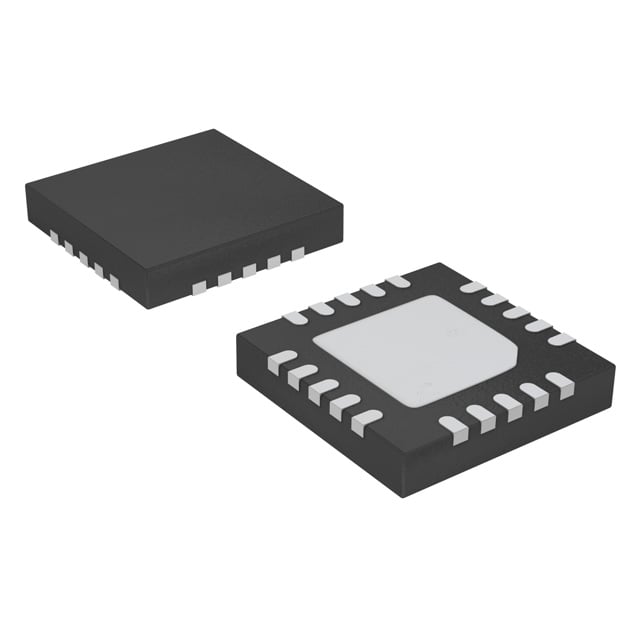
ICGOO电子元器件商城为您提供A4491EESTR-T由Allegro设计生产,在icgoo商城现货销售,并且可以通过原厂、代理商等渠道进行代购。 A4491EESTR-T价格参考。AllegroA4491EESTR-T封装/规格:PMIC - 稳压器 - DC DC 开关稳压器, 可调式 降压 开关稳压器 IC 正 0.8V 3 输出 20-WFQFN 裸露焊盘。您可以下载A4491EESTR-T参考资料、Datasheet数据手册功能说明书,资料中有A4491EESTR-T 详细功能的应用电路图电压和使用方法及教程。
| 参数 | 数值 |
| 产品目录 | 集成电路 (IC) |
| 描述 | IC REG BUCK ADJ TRPL 20QFN |
| 产品分类 | |
| 品牌 | Allegro MicroSystems, LLC |
| 数据手册 | |
| 产品图片 |
|
| 产品型号 | A4491EESTR-T |
| PWM类型 | 电流模式 |
| rohs | 无铅 / 符合限制有害物质指令(RoHS)规范要求 |
| 产品系列 | - |
| 供应商器件封装 | 20-QFN(4x4) |
| 其它名称 | 620-1516-2 |
| 包装 | 带卷 (TR) |
| 同步整流器 | 无 |
| 安装类型 | 表面贴装 |
| 封装/外壳 | 20-WFQFN 裸露焊盘 |
| 工作温度 | -40°C ~ 85°C |
| 标准包装 | 1,500 |
| 电压-输入 | 4.5 V ~ 23 V |
| 电压-输出 | 可调 |
| 电流-输出 | - |
| 类型 | 降压(降压) |
| 输出数 | 3 |
| 输出类型 | 可调式 |
| 配用 | /product-detail/zh/APEK4491EES-01-T-DK/620-1571-ND/4860637 |
| 频率-开关 | 550kHz |


- 商务部:美国ITC正式对集成电路等产品启动337调查
- 曝三星4nm工艺存在良率问题 高通将骁龙8 Gen1或转产台积电
- 太阳诱电将投资9.5亿元在常州建新厂生产MLCC 预计2023年完工
- 英特尔发布欧洲新工厂建设计划 深化IDM 2.0 战略
- 台积电先进制程称霸业界 有大客户加持明年业绩稳了
- 达到5530亿美元!SIA预计今年全球半导体销售额将创下新高
- 英特尔拟将自动驾驶子公司Mobileye上市 估值或超500亿美元
- 三星加码芯片和SET,合并消费电子和移动部门,撤换高东真等 CEO
- 三星电子宣布重大人事变动 还合并消费电子和移动部门
- 海关总署:前11个月进口集成电路产品价值2.52万亿元 增长14.8%


PDF Datasheet 数据手册内容提取
A4491 Triple Output Step-Down Switching Regulator Features and Benefits Description ▪ Three buck converters in a single package Designed to provide the power supply requirements of printers, ▪ 4.5 to 23 V input voltage range office automation, industrial, and portable equipment, the ▪ 550 kHz fixed frequency A4491 provides three high current, high performance, switching ▪ Multiphase switching for smaller components and regulator outputs in a single package, saving space, cost and lower EMI component count. ▪ Independent control of each converter for sequencing and shutdown control High frequency switching allows selection of inexpensive ▪ Power-on-reset flag with adjustable delay inductors and small ceramic output capacitors. The turn-on ▪ Internal compensation to minimize components and cycles of the regulators are interleaved to minimize stresses on simply design the input capacitors and to reduce EMI. Independent Enable ▪ 4 × 4 mm QFN Package, small PCB footprint pins simplify power sequencing and shutdown capabilities, and a power-on-reset (POR) circuit with user configurable delay indicates when enabled regulators are in specification. Continued on the next page… Package: 20-contact QFN (suffix ES) Applications: ▪ Photo, inkjet, and portable printers • Set-top boxes • Tablet computing • Other Consumer Electronics applications • Point-of-sale applications • Security systems Approximate size • Gaming machines • Other Industrial applications Typical Application VBB VDD CP1 CP2 VCP VBB1 PORZ LX1 CPOR VREG1 FB1 Microcontroller or A4491 Controller Logic VBB2 ENB1 ENB2 LX2 ENB3 VREG2 FB2 PGND VBB3 LX3 GND VREG3 FB3 4491-DS, Rev. 1
A4491 Triple Output Step-Down Switching Regulator Description (continued) The POR flag also indicates when the input voltage drops below Output current capability is ≈ 4.5A total for all 3 outputs, depending specification, giving the system controller advance warning while on the combinations of V and each V level. IN OUT the switchers continue to operate down to the shutdown level. The A4491 is provided in a 20-contact, 4 mm × 4 mm, 0.75 mm Internal diagnostics provide comprehensive protection against nominal overall height QFN, with exposed pad for enhanced overloads, input undervoltages, and overtemperatures. thermal dissipation. It is lead (Pb) free, with 100% matte tin leadframe plating. Selection Guide Operating Temperature Range Part Number Packing (°C) A4491EESTR-T 1500 pieces per 7-in. reel –40 to 85 Absolute Maximum Ratings (reference to GND) Characteristic Symbol Notes Rating Units Load Supply Voltage V 24 V BB LX1, LX2, and LX3 Pins V –1 to 24 V LXn PORZ and VDD Pins V –0.3 to 7 V IN ENBx Pin Input Current I Driven by a current-limited voltage source 1 mA ENBx Operating Ambient Temperature T Range E –40 to 85 ºC A Maximum Junction Temperature T (max) 150 ºC J Storage Temperature T –55 to 150 ºC stg Recommended Operating Conditions Characteristic Symbol Conditions Min. Typ. Max. Units To operate at V < 6 V, connect V BB DD Load Supply Voltage V supply to the V supply. See Powering 4.5 – 23 V BB BB Configurations section. LX1, LX2, and LX3 Pins V –0.7 – 23 V LXn Operating Ambient Temperature T –40 – 85 ºC A Junction Temperature T –40 – 125 ºC J Thermal Characteristics may require derating at maximum conditions, see application information Characteristic Symbol Test Conditions* Value Units Package Thermal Resistance R On 4-layer PCB based on JEDEC standard 37 ºC/W θJA *Additional thermal information available on the Allegro website. Allegro MicroSystems, LLC 2 115 Northeast Cutoff Worcester, Massachusetts 01615-0036 U.S.A. 1.508.853.5000; www.allegromicro.com
A4491 Triple Output Step-Down Switching Regulator Functional Block Diagram C2 47 nF C C P P VBB 1 2 VDD Regulator Charge Pump VCP C1 C3 100 nF Switch 47 nF VBB VBB1 C4 VBB Bias Supply VCP 10 μF VREG1 L1 5 V / 1.5 A LX1 100 kΩ 15 μH C5 Switcher #1 D1 Switcher Control ENB1 SS R1 10 μF FB1 R2 VBB2 C6 VCP 10 μF VREG2 L2 3.3 V / 1.5 A LX2 ENB2 SS Switcher #2 10 μH C7 C8 D2 VDD Switcher Control 10 μF 10 μF R3 FB2 PORZ R4 POR Block VBB3 C9 CPOR C14 10 μF VREG3 VCP L3 1.0 V / 1.5 A 470 nF LX3 4.7 μH C10 C11 C12 C13 ENB3 SS Switcher #3 D3 Switcher Control 10 μF 10 μF 10 μF 10 μF R5 FB3 PGND GND R6 Note: All capacitors ceramic X5R. Allegro MicroSystems, LLC 3 115 Northeast Cutoff Worcester, Massachusetts 01615-0036 U.S.A. 1.508.853.5000; www.allegromicro.com
A4491 Triple Output Step-Down Switching Regulator Pin-out Diagram 1 1 3 NB X1 BB BB X3 E L V V L 0 9 8 7 6 2 1 1 1 1 FB1 1 15 ENB3 VDD 2 14 FB3 GND 3 PAD 13 PGND FB2 4 12 CP1 ENB2 5 11 CP2 6 7 8 9 10 2 2 R Z P X B O R C L VB CP PO V Terminal List Number Name Function 1 FB1 Feedback REG1 2 VDD Bias supply 3 GND1 Ground 4 FB2 Feedback REG2 5 ENB2 Enable REG2, logic input, active high 6 LX2 Switch node REG2 7 VBB22 Input supply for REG2 8 CPOR POR delay adjustment 9 PORZ Power on reset output, active low 10 VCP Charge pump reservoir 11 CP2 Charge pump capacitor terminal 12 CP1 Charge pump capacitor terminal 13 PGND1 Ground for charge pump circuitry 14 FB3 Feedback REG3 15 ENB3 Enable REG3, logic input, active high 16 LX3 Switch node REG3 17 VBB32 Input supply for REG3 18 VBB12 Input supply for REG1 19 LX1 Switch node REG1 20 ENB1 Enable REG1, logic input, active high – PAD3 Exposed pad for enhanced thermal dissipation 1GND and PGND should be connected externally. 2The three VBBx pins should be connected together externally. 3Thermal pad should be connected to the ground (0 V) plane using thermal vias. Allegro MicroSystems, LLC 4 115 Northeast Cutoff Worcester, Massachusetts 01615-0036 U.S.A. 1.508.853.5000; www.allegromicro.com
A4491 Triple Output Step-Down Switching Regulator ELECTRICAL CHARACTERISTICS* at T = 25°C, V = 12 V, V supplied externally, unless noted otherwise A BB DD Characteristics Symbol Test Conditions Min. Typ. Max. Units General ENBx = high, I = 0 mA, V = 12 V, I LOAD BB – 1 2 mA VBB Quiescent Current BBON current drawn by feedback resistors ignored I ENBx = 0 V – 1 – μA BBOFF VDD Supply Range V 3.3 – 5.5 V DD ENBx = high – – 6 mA VDD Quiescent Current I DD ENBx = 0 V – 1 – μA REG1, REG2, and REG3 Feedback Input Bias Current I –400 –100 100 nA BIAS Feedback Voltage V With respect to 0.8 V target voltage; V = 6 to 23 V – ±1 – % FB BB Fixed Frequency f 470 550 630 kHz SW Maximum Duty Cycle DC 90 – – % max Minimum Duty Cycle DC – 5 – % min T = 25°C, I = 1.5 A, V = 6.0 V – 450 – mΩ J LOAD BB T = 125°C, I = 1.5 A, V = 6.0 V – 700 – mΩ J LOAD BB Buck Switch On-Resistance R DS(on) T = 25°C, I = 1.5 A, V = 4.5 V – 560 – mΩ J LOAD BB T = 125°C, I = 1.5 A, V = 4.5 V – 870 – mΩ J LOAD BB Current Limit Threshold I Peak current through switch with D = 0.9 2.0 A LIM Soft Start Duration t 0.625 1.25 1.875 ms ss Logic Inputs and Outputs V – – 0.8 V IL ENBx Input Voltage V 2.0 – – V IH ENBx Input Hysteresis V 300 500 – mV I(hys) ENBx Input Current I V ≤ 5 V –1 – 1 μA IL IH PORZ Output (Open Drain) V I = 1 mA, fault asserted – – 0.4 V PORZL PORZL PORZ Output Leakage Current I V = 5 V, fault not asserted –1 – 1 μA PORZH PORZ Power-On Reset Duration t C = 470 nF 75 115 155 ms POR POR Protection VREGx Undervoltage Lockout Startup V FB1, FB2, and FB3 rising – 85 – %V REGUV(su) FB VREGx Undervoltage Lockout Shutdown V FB1, FB2, and FB3 falling – 80 – %V REGUV(sd) FB VREGx Undervoltage Lockout V – 5 – % Startup Hysteresis REGUV(suhys) V No external VDD supply, V rising 3.7 4.3 4.7 V BBUV(su) BB VBB Undervoltage Lockout Startup V External VDD supply, V rising 3.8 4.2 4.6 V BBCPUV(su) BB V No external VDD supply, V falling 3.6 4.1 4.7 V BBUV(sd) BB VBB Undervoltage Lockout Shutdown V External VDD supply, V falling 3.0 3.5 4.3 V BBCPUV(sd) BB VBB Undervoltage Lockout VBBUV(sdhys) No external VDD supply – 500 – mV Shutdown Hysteresis V External VDD supply – 600 – mV BBCPUV(sdhys) V falling (forces PORZ low); switchers continue VBB Undervoltage Warning Threshold V BB – 3.6 – V BBUV(por) to operate Junction Overtemperature Shutdown T Temperature rising – 165 – °C JTSD Junction Overtemperature Shutdown T Recovery = T –T – 15 – °C Hysteresis JTSD(hys) JTSD JTSD(hys) *For input and output current specifications, negative current is defined as coming out of (sourcing) the specified pin. Allegro MicroSystems, LLC 5 115 Northeast Cutoff Worcester, Massachusetts 01615-0036 U.S.A. 1.508.853.5000; www.allegromicro.com
A4491 Triple Output Step-Down Switching Regulator Functional Description Basic Operation auto-restart under control of the soft start circuit after the thermal The A4491 contains three fixed frequency, buck switching con- disable condition is removed, and assuming all other conditions verters with peak current-mode control, including slope compen- are met. See the Shutdown section for more information. sation. Each converter can be independently turned on and off via Power Configuration the enable inputs (EN1, EN2, and EN3), which are active high. The A4491 supports alternative schemes for providing logic sup- When enabled, the corresponding output is brought-up under the ply voltage on the VDD pin. In addition, the IC can be powered control of a soft start routine, which avoids output voltage over- up and down using either the VBB or ENB pins. shoot and minimizes input inrush current. Powering VDD To minimize power dissipation, especially at The output voltage is typically divided down by an external high input voltages, it is recommended that an external sup- potential divider, and is compared against an internal reference ply be applied to the VDD input pin. Typically, this voltage is voltage to produce an error signal, also known as the current derived from one of the three regulated outputs that are set-up for demand signal. The current signal through the buck switch is between 3.3 and 5 V (V ). REGx converted into a voltage. This signal is then compared against the current demand signal to create the required duty cycle. Another advantage of powering the VDD externally is that the VBB undervoltage lockout level is lowered. To maximize the At the beginning of each switching cycle, the buck switch is run time of the switchers during a VBB power-down condition, turned on. When the current signal through the switch reaches the two alternative undervoltage shutdown conditions are supported, level of the current demand signal, the on-time of the switch is depending on which VDD-powering configuration has been terminated. On the next switching cycle, the switch is turned on implemented. When no external VDD is applied, the minimum again and the cycle is repeated. V , V ,is 4.1 V typical. When an external VDD is BB BBUV(sd) applied, the minimum V , V , is 3.5 V typical. One shared clock is used to define the switching frequency for BB BBCPUV(sd) each regulator. Each of the three switching cycles (REG1, REG2, One note of caution when deriving VDD from a VREG output: and REG3) are phase shifted with respect to one another by 120° during initial application of V , the internal bias supply auto- BB in an attempt to minimize the pulsed current drawn from the matically starts from the internal regulator because VREG has not input filter capacitors. Under certain conditions, for example at yet reached regulation. This means the startup threshold is deter- low VBB conditions and relatively high user-set output voltages, mined by VBBUV(su) (4.3 V typical) because there is no external switching overlap between channels is inevitable. VDD. When VREG has begun to supply VDD externally, the shutdown threshold reduces to V (3.5 V typical). This Under conditions, such as light loads or high V voltages, that BBCPUV(sd) BB assumes that V is present. cause duty cycles (DC) of less than the minimum value, the REG converter enters a pulse-skipping mode to ensure regulation is Powering Up and Down with VBB Referring to figure 1, maintained. each of the enable inputs (ENBx) are held high by being tied to the V rail via a 100 kΩ resistor and the VDD is supplied from A charge pump regulator is provided to ensure a sufficient gate BB one of the regulator outputs. When the V voltage reaches the drive is available for all three power switches across the full input BB minimum threshold, V , the charge pump supply (VCP) voltage range. This regulator allows operation even at very wide BBUV(su) ramps up. When V + V has reached the minimum thresh- operating duty cycles. On initial power-up, an internal regulator BB CP old V , the soft start routines are initiated (t ) for all is used to provide the bias supply for on-chip control functions. BBCPUV(su) SS three regulator channels (VREGx). When all three regulators Each regulator channel utilizes pulse-by-pulse current limiting in have reached the 85% FBx threshold, the power-on-reset timer the event of either a short circuit or an overload. If the overload is initiated. After the power-on-reset period, t , has elapsed, POR is applied long enough, the IC temperature may rise sufficiently PORZ goes high, indicating that all the regulators and V are in BB to cause the thermal shutdown circuit to operate. The part will specification. Allegro MicroSystems, LLC 6 115 Northeast Cutoff Worcester, Massachusetts 01615-0036 U.S.A. 1.508.853.5000; www.allegromicro.com
A4491 Triple Output Step-Down Switching Regulator VBBUV(su) VBBUV(por) VBB 0V V +5.5 V BB V BBCPUV(su) VBB+VCP V BBCPUV(sd) VREG1 85%FB1 VREG2 VREG3 85%FB2 85%FB3 PORZ tSS tPOR Figure 1. Timing diagram for powering up and down using the VBB pin VBB 0V ENB1 ENB2 ENB3 VREG1 85%FB1 VREG2 VREG3 85%FB2 80%FB2 85%FB2 85%FB3 tSS tPOR tSS tPOR tPOR t PORZ SS Figure 2. Timing diagram for powering up and down using the ENB pin Allegro MicroSystems, LLC 7 115 Northeast Cutoff Worcester, Massachusetts 01615-0036 U.S.A. 1.508.853.5000; www.allegromicro.com
A4491 Triple Output Step-Down Switching Regulator When the V voltage starts to fall below the undervoltage warn- PORZ signal, it is recommended that the system be designed such BB ing level, V , of 3.6 V typical, the PORZ flag resets. that all three regulator channels are within specification before BBUV(por) This gives advance warning to the system controller that the V t has elapsed. BB POR voltage is falling. Note that this feature is only guaranteed when If any regulator channel drops below 80% FB, the PORZ signal VDD is supplied externally. During this interval, the three switch- will be reset. If the voltage then recovers to within 85% FB, the ers continue to operate. POR timer is initiated again. Note that a soft start is not initiated While V falls further, the VCP supply also tends to fall, which when the feedback voltage drops below the 80% FB level. This is BB degrades the drive voltage to the series switches. In addition, to allow a rapid auto-restart in the event of an overload or similar the higher voltage rails start to fall out of regulation first, as the fault. If a soft start is required, it is recommended that on receipt corresponding maximum duty cycle (D ) for these particular of the PORZ reset signal, the system controller disables and then max converters is reached. re-enables the relevant regulator channels again. As soon as the last regulator is disabled the PORZ signal is reset. The regulators that have the lower output voltages achieve some level of steady state, before the A4491 powers down when all Power on Reset The power-on-reset duration, t , is deter- POR of the corresponding V undervoltage thresholds have been mined by selecting an appropriate capacitor connected to the BB reached. For example, it may be possible for a 1 V output to CPOR pin. The value of t can be determined by the following POR continue to operate down to a V of 3.4 V typical, if the VDD formula: BB supply is derived externally. The extent of this effect depends on t = 2.131 ×10⁵ × C . (1) POR POR a myriad of factors, including input and output filter capacitance, The PORZ output goes high when both V is above the under- output loads, gate drive amplitude, MOSFET R , and so BB DS(on) voltage warning levels, and the FB pins of the regulators that are forth. enabled are > 85% of the V voltage. REG Powering Up and Down with Enable Referring to figure 2, Because the external capacitor is charged via a 5 μA current V is present and the UVLO start-up thresholds, V BB BBUV(su) source, care must be taken in the layout to avoid additional leak- and V have been reached. Each of the regulators are BBCPUV(su) age paths. The capacitor should be positioned adjacent to the enabled in turn. Initially, VREG1 is enabled and is brought-up CPOR pin, and the ground connection to the A4491 GND pin under the control of the soft start circuit (t ). Before VREG1 SS should be as short as possible. reaches 85% FB1, VREG2 is enabled and is brought-up under a separate soft start control. It is recommended that the t period be set to exceed the POR start-up phases of all three regulators, to avoid the possibility of When both regulators have reached their respective 85% FB multiple triggerings of the PORZ output. thresholds, the power-on-reset (POR) timer is initiated. Note that the POR timer is only enabled after all of the enabled regulators Output Voltage Selection The output voltage on each of the reach their corresponding 85% FB levels. After the power-on- three regulators is set by the following relationship, shown here reset time, tPOR , has elapsed, if the FB levels of VREG1 and for the VREG1 channel: VREG2 are not below their respective 80% FB levels, then the ⎛V ⎞ PORZ signal will go high. R1 = R2 ⎜⎜ VREG1 – 1 ⎟⎟ , (2) ⎝ FB ⎠ At some point later, if VREG3 is enabled, then the PORZ is reset and VREG3 is brought-up under the control of the soft start where R2 (connected between GND and the FB1 pin) should circuit. When the 85% FB3 threshold is reached, the POR timer be a value between 4.7 and 12 kΩ. R1 is connected between the is initiated. After t has elapsed, if all the FB levels are above output rail and the FB1 pin. V is the set output regulator POR REG1 their respective 80% FB levels, then the PORZ signal will go voltage. V is the reference voltage. FB high. The tolerances of the feedback resistors influence the voltage set- Note that if any regulator channel is not enabled, the channel point. It is therefore important to consider the tolerance selection will not influence PORZ. To avoid multiple signal changes of the when targeting an overall regulation figure. Allegro MicroSystems, LLC 8 115 Northeast Cutoff Worcester, Massachusetts 01615-0036 U.S.A. 1.508.853.5000; www.allegromicro.com
A4491 Triple Output Step-Down Switching Regulator The bias current, I , flowing out of the FB1 node into R2, will to check the implications on the thermal performance. See the BIAS introduce a small voltage offset to the output. Thermal Considerations section. Enable Each regulator channel can be individually enabled via Component Selection the corresponding ENBx pin. If any channel is required to start- up automatically after the VBB voltage is applied, that particu- Inductor The inductance value, L, determines the ripple current. lar channel should have the ENB pin tied to the VBB rail via a It is important to ensure that the minimum current limit is not pull up resistor. exceeded under worst-case conditions: V (min), I (max), BB LOAD f (min), and L(min). This resistor should be selected to limit the current to less than SW the maximum specified value, 1 mA. This prevents the internal It is recommended that gapped ferrite solutions be used as protection clamps from turning on. It is recommended that a opposed to powdered iron solutions, the latter of which exhibit 100 kΩ pull-up resistor be used. This would ensure the current relatively high core losses that can have a large impact on long remains below the maximum value when V = 24 V. term reliability. BB Soft Start Each regulator channel contains a soft start circuit. A Inductors are typically specified at two current levels, rms cur- soft start cycle is initiated when the appropriate regulator enable rent and saturation current. With regard to the rms current, it is input is set to high; the V , charge pump, and bias supply volt- important to understand how the rms current level is specified, BB ages are above the minimum values; and no thermal shutdown in terms of ambient temperature. Some manufacturers quote an condition exists. Note that an overload or short circuit will not ambient only, whilst others quote a temperature that includes a cause a soft start cycle, unless a thermal shutdown event occurs. self-induced temperature rise. For example, if an inductor is rated for 85°C and includes a self-induced temperature rise of 25°C During a soft start cycle, the reference voltage is ramped from at maximum load, then the inductor cannot be safely operated 0 to 0.8 V typical, which in turn forces the current demand signal beyond an ambient temperature of 60°C at full load. The rms cur- to increase in a linear fashion. rent can be assumed to be simply the maximum load current, with Shutdown All converter channels are disabled in the event of perhaps some margin to allow for overloads, and so forth. either a thermal shutdown event or an undervoltage on VBB The first stage of determining the inductor value is to specify a (V or V ). BBUV(sd) BBCPUV(sd) peak-to-peak ripple current of typically about 20% to 25% of the As soon as the above fault conditions have been removed, and maximum load. assuming the ENB inputs are enabled, the appropriate channels will auto-restart under control of the soft start. 5.0 4.5 Current Limit The typical peak current limit for each channel is 4.0 specified as 2.5 A minimum, with a duty cycle of 0.9. The mini- A) 3.5 mum current limit occurs at maximum duty cycle (0.9), because mit ( 3.0 the slope compensation has a maximum effect under this condi- Li 2.5 tion. As the duty cycle reduces, the current limit increases. This ent 21..05 rr means for applications that operate with a narrow duty cycle, it is u 0.5 C possible to operate with a load current greater than 2.0 A. 1.0 0.5 Figure 3 illustrates the typical peak current limit versus duty 0 cycle. For example, it is possible to operate with a peak current 0 20 40 60 80 100 limit of 3.75 A with a duty cycle of 0.3. Duty Cycle (%) As well as ensuring the peak current limit is not exceeded, under worst case load and input voltage conditions, it is also important Figure 3. Current limit versus duty cycle Allegro MicroSystems, LLC 9 115 Northeast Cutoff Worcester, Massachusetts 01615-0036 U.S.A. 1.508.853.5000; www.allegromicro.com
A4491 Triple Output Step-Down Switching Regulator The maximum peak-to-peak ripple current, I , occurs at the The output capacitor determines the output voltage ripple and is RIPPLE maximum input voltage. Therefore the duty cycle, D, should be used to close the control loop. To guarantee stability, the capaci- tance has to increase as the output voltage is reduced. This is found under these conditions (for the VREG1 channel): actually reasonable from a ripple voltage point of view, as the V +V ripple voltage is typically specified as a percentage of output D(min) = REG1 f . (3) V (max)+V voltage. BB f The following table outlines what the minimum output capaci- where V is the forward voltage drop of the recirculation diode. f tance should be for a given output voltage: The required inductance can be found: Output Voltage Minimum Output Capacitance V (max) – V 1 (V) (μF) L (min)= BB REG1×D(min)× , (4) I f (min) 5 10 RIPPLE SW 3.3 20 Note that the manufacturers inductance tolerance should also 1.8 to 2.5 30 be taken into account. This value may be as high as ±20%. The <1.8 40 peak-to-peak current should not exceed 1 A, to avoid instability Capacitance values with greater than the above values can be in the innermost circuit loops due to insufficient slope compensa- used with the effect of reducing the bandwidth. This may be nec- tion. essary in systems that have extremely low ripple/noise require- ments. The maximum peak current can be found from to ensure that the saturation current level of the chosen inductor is not exceeded: The output ripple is largely determined by the output capacitance and the effects of ESR and ESL can largely be ignored assuming I I = I + RIPPLE . (5) good layout practice is observed. sat LOAD 2 The output voltage ripple can be approximated to: Recommended inductor manufacturers and ranges are: I V ≈ RIPPLE , (6) • Taiyo Yuden: NR6045 series for 1.5 A outputs RIPPLE 8 × f × C SW OUT • Taiyo Yuden: NRG4026 series for 1.0 A outputs When using ceramic capacitors, there is generally no need to con- sider the current carrying capability due to the negligible heating • Sumida: CDH74 series for 1.5 A outputs effects of the ESR. Also, the rms current flowing into the output Output Capacitor In the interests of size, cost and perfor- capacitor is extremely low. mance, it is highly recommended that ceramic X5R or X7R Input Capacitor Again it is highly recommended that ceramic, capacitor types be used. When using ceramic capacitors another X5R or X7R capacitors be used. important consideration is the E-field effects on the actual value The value of the input capacitance determines the amount of of the capacitor. To minimize the effects of the capacitance current ripple (EMI) that appears at the source (V supply) reducing with output voltage, it is recommended that the working BB terminals. The amounts of current flowing in and out of the input voltage of the capacitor be considerably more than the set output capacitor depend on the relative impedances between the input voltage. As a suggestion, it is recommended that 6.3 V-rated capacitor impedance and the source impedance. To achieve a low capacitors should be used for output voltages of 3.3 V and below. impedance filter solution it is recommended to place at least two For output voltages of 5 V, a 10 V-rated capacitor should be used. capacitors in parallel. Allegro MicroSystems, LLC 10 115 Northeast Cutoff Worcester, Massachusetts 01615-0036 U.S.A. 1.508.853.5000; www.allegromicro.com
A4491 Triple Output Step-Down Switching Regulator Again, there is generally no need to consider the heating effects The following steps can be used as a guideline for determining a of the rms current flowing through the ESR. Also, the phase- suitable thermal solution. It should be noted that this process is shifting of the input current drawn by each of the regulators helps usually an iterative one to achieve the optimum solution. These to reduce the overall rms current. factors can be considered as follows: Flyback Diode This diode conducts during the switch off-time. Step 1. Estimate the maximum ambient temperature, T (max) , of A A Schottky diode is recommended to minimize both the forward the application. drop and switching losses. Step 2. Define the maximum junction temperature, T(max). Note J The worst case dissipation occurs at maximum VBB , when the that the absolute maximum is 150°C. duty cycle, D, is a minimum. The average current through the diode can be found: Step 3. Determine the worst case power dissipation, PD(max). The evaluation should consider these at maximum load and mini- I = I × (1 – D(min)) . (7) DIODE(av) LOAD mum V . Contributors are switch static and dynamic losses, and BB The forward voltage drop, Vf , can be found from the diode control losses. These are described in the following sections characteristics by using the actual load current (not the average Switch Static Losses The following steps can be used to current). determine switch static losses: The static power dissipation can be found: Estimate the maximum duty cycle: PSTAT = ILOAD(av) × Vf . (8) D(max) = VREG + Vf , (9) It is also important to take into account the thermal rating of V (min) + V BB f the package, RθJA , and the ambient temperature, to ensure that enough heatsinking is provided to maintain the diode junction where V is the forward voltage drop of the Schottky diode under f temperature within the safe operating area for the device. the given load current. To minimize the heating effects from the A4491 on the diode and Estimate the R of the each regulator switch at the given DS(on) vice-versa, it is recommended that the diode be mounted on the junction temperature: reverse side of the printed circuit board. ⎛ T – 25 ⎞ R =R ⎜1+ J ⎟ . Support Components POR capacitor (C11), charge pump DS(on)TJ DS(on)25C ⎜ 200 ⎟ (10) ⎝ ⎠ capacitor (C1), reservoir capacitor (C2) and VDD filter capacitor (C12) should be ceramic X5R or X7R. Note that if the V range is restricted to between 4.5 and 5.5 V, BB the R increases. For example, the R at 25°C with a Thermal Considerations DS(on) DS(on) V greater than 6 V is 450 mΩ typical, as stated in the Electri- To ensure the A4491 operates in the safe operating area, which BB cal Characteristics table. Under the same temperature conditions, effectively means restricting the junction temperature to less than with the V = 4.5 V, the R is 560 mΩ typical. For VBB 150°C, several checks should be made. The general approach BB DS(on) voltages between 4.5 and 6 V, the R can be found by linear is to work out what thermal impedance (R ) is required to DS(on) JA approximation. For more information on operating the A4491 maintain the junction temperature at a given level, for a particular between a V voltage of 4.5 and 5.5 V, see the Power Configu- power dissipation. BB rations section. Another factor worth considering is that other power dissipating components on the system PCB may influence the thermal per- The static loss for each switch can be determined: formance of the A4491. For example, the power loss contribution P = I 2 × D(max) × R , (11) from the recirculation diode and the sense resistor may cause the STAT LOAD DS(on)TJ junction temperature of the A4491 to be higher than expected. where I is the load for that particular regulator channel. LOAD Allegro MicroSystems, LLC 11 115 Northeast Cutoff Worcester, Massachusetts 01615-0036 U.S.A. 1.508.853.5000; www.allegromicro.com
A4491 Triple Output Step-Down Switching Regulator Switch Dynamic Losses The following can be used to deter- (a) Switch static losses mine switch dynamic losses: 5+0.4 V duty cycle, D = =0.84 REG1 1 6+0.4 Both turn on and turn off losses can be estimated: 3.3+0.4 V duty cycle, D = =0.58 REG2 2 6+0.4 I 1.8+0.4 P =V (min) LOAD 30 10–9 f , (12) V duty cycle, D = =0.34 DYN BB 2 SW REG3 3 6+0.4 The R of each switch can be found: where f is the switching frequency. DS(on) SW ⎛ ⎞ 115– 25 Control Losses The following steps can be used to determine RDS(on)TJ = 450×10–3 ⎜⎜1+ 20 0 ⎟⎟ = 0.653 Ω ⎝ ⎠ control losses: The static loss of each switch can be found: P = I × V , (13) VBB BBON BB P = 12 × 0.84 × 0.653 = 0.55 W STAT1 where IBBON is the quiescent current assuming all three regulators PSTAT2 = 12 × 0.58 × 0.653 = 0.379 W are on. P = 0.82 × 0.34 × 0.653 = 0.14 W STAT3 (b) Switch dynamic losses P = I × V , (14) VDD VDD DD 1 where I and is the quiescent current on VDD. P =6 30 10–9 500 103 = 0.045 W VDD DYN1 2 1 Total Losses The total losses can now be estimated: P =6 30 10–9 500 103 = 0.045 W DYN2 2 0.8 P =6 30 10–9 500 103 = 0.036 W P = P + P + P DYN3 2 TOTAL STAT1 STAT2 STAT2 +P +P + P (c) Control losses DYN1 DYN2 DYN3 P = 0.005 × 6 = 0.03 W +P + P . (15) VBB VBB VDD P = 0.001 × 3.3 = 0.003 W VDD Thermal Impedance The thermal impedance required for the (d) The total power dissipation can now be found: solution can now be determined: P = 0.55 + 0.379 + 0.14 + 0.045 TOTAL T – T + 0.045 + 0.036 + 0.03 + 0.003 = 1.228 W R(cid:81)JA= PJ A . (16) TOTAL (e) The thermal impedance required for the solution can be found: Example 115– 70 R = = 36.6 °C/W (cid:81)JA 1.228 Selected parameters: V (min) = 6 V For this particular solution a high thermal efficiency board is BB required to ensure the junction temperature is kept below 115°C. V = 5 V at 1 A REG1 For maximum effectiveness, the PCB pad area underneath the V = 3.3 V at 1 A REG2 thermal pad of the A4491 should be exposed copper. Several VREG3 = 1.8 V at 800 mA thermal vias (say between 4 and 8) should be used to connect T = 70°C the thermal pad to the internal ground plane. If possible, an A additional thermal copper plane should be applied to the bottom T = 115°C J side of the PCB and connected to the thermal pad of the A4491 V = 0.4 V f through the vias. Allegro MicroSystems, LLC 12 115 Northeast Cutoff Worcester, Massachusetts 01615-0036 U.S.A. 1.508.853.5000; www.allegromicro.com
A4491 Triple Output Step-Down Switching Regulator This calculation assumes no thermal influence from other compo- mize interference effects of ground noise from the power circuitry. nents. If possible, it is advisable to mount the flyback diodes on Figure 4 illustrates the recommended grounding architecture. the reverse side of the printed circuit board. Ensure low imped- To avoid ground bounce and offset issues, it is highly recom- ance electrical connections are implemented between board mended that the ground referenced feedback resistors (R2, R4, layers. and R6) should be connected as close to the GND connection of PCB Layout Guidelines The ground plane is largely dictated the A4491 as possible. by the thermal requirements described in the previous section. A local quiet ground plane around these components can be The ground referenced power components should be referenced implemented, however, this ground plane should have a high to a star ground, located away from the A4491 to minimize impedance connection to the star connection of the power stages. ground bounce issues. If a ground plane is used, it is recommended that it does not A small, local, relatively quiet ground plane near the A4491 should overlap the switching nodes (LX1, LX2, and LX3) to avoid the be used for the ground referenced support components, to mini- possibility of noise pick-up. To minimize the possibility of noise injection issues, it is recommended to isolate the ground plane around high impedance nodes such as: FBx, ENBx and CPOR. In terms of grounding the power components, a star connection A4491 Support should be made to minimize the ground loop impedances. Note Components Power Circuitry that although a ground plane may be required to meet the thermal Cin D Cout characteristics of the solution it is still imperative to implement A4491 a ground star connection for the power components. The ground for the charge pump (PGND) should be connected to the thermal Local “Quiet’ GND PGND vias. Ground Plane Star Connection Figures 5 and 6 below illustrates the importance of keeping the Thermal Vias ground connections as short as possible and forming good star Internal Ground Plane connections. Figure 5 also illustrates the current conduction paths during the on-cycle of the switching FET. The following points should be Figure 4. Ground plane configurations noted: • The capacitor C should be placed as close as possible to the IN Q LX L Q LX L VBB VREG VBB VREG D D CIN COUT C COUT IN RLOAD RLOAD Star Connection Star Connection Figure 5. FET on-cycle current conduction paths Figure 6. FET off-cycle current conduction paths Allegro MicroSystems, LLC 13 115 Northeast Cutoff Worcester, Massachusetts 01615-0036 U.S.A. 1.508.853.5000; www.allegromicro.com
A4491 Triple Output Step-Down Switching Regulator VBB terminals. The capacitance should be split between the VBB switching FET and the inductor. terminals for V and V and the VBB terminal for V . REG1 REG3 REG2 • Support components: POR capacitor (C11), charge pump ca- The VBB terminals for V and V should be connected REG1 REG2 pacitor (C1), reservoir capacitor (C2), and VDD filter capacitor via short and wide traces to the VBB terminal for V . REG3 (C12) should be located as close as possible to their respective • Each inductor should be connected as close as possible to the terminal connections. The ground referenced capacitors should respective switching FET (LX1, LX2, and LX3) and output be connected as close to the GND terminal as possible. capacitors. Powering Configurations The following three diagrams show Figure 6 shows the current conduction path during the off-cycle typical configurations for providing power to the application. The of the switching FET. The following points should be noted: middle diagram corresponds to the typical application shown on • The diode D should be placed as close as possible to both the the front page. Only VBB supplied VDD applied externally (first option) VDD applied externally (second option) 6 to 23 V 6 to 23 V 4.5 to 5.5 V VBB VBB VBB L L L LX VREG LX VREG LX VREG VDD VDD VDD D C D C D C Comments: Comments: Comments: - Simple configuration, only one supply required - Increased power losses at higher VBB voltages - Reduced power losses at higher VBB voltages - Power restricted as VBB < 6 V, due to increase in - V(tyBBp isctaalr)t-up = 4.3 V (typical), shutdown = 4.1 V - V(tyBBp isctaalr)t.- uInp t =h i4s. 2c aVs e(t,y tphiec aslt)a, rsth-uuptd tohwrens h=o 3ld.5 V - V RBDBS s(otan)r to-uf pb u=c 4k. 2s wVi t(ctyhpeiscal), shutdown = 3.5 V (typical) (VBBUV(su)) is lower because VREG is not present Allegro MicroSystems, LLC 14 115 Northeast Cutoff Worcester, Massachusetts 01615-0036 U.S.A. 1.508.853.5000; www.allegromicro.com
A4491 Triple Output Step-Down Switching Regulator Package ES, 20-Pin QFN 0.30 4.00 ±0.15 20 0.50 20 0.95 1 2 A 1 2 4.00 ±0.15 2.60 4.10 2.60 4.10 21X D SEATING C C PCB Layout Reference View 0.08 C PLANE +0.05 0.25–0.07 0.75 ±0.05 For Reference Only (reference JEDEC MO-220WGGD) 0.50 Dimensions in millimeters Exact case and lead configuration at supplier discretion within limits shown A Terminal #1 mark area B Exposed thermal pad (reference only, terminal #1 identifier appearance at supplier discretion) 0.40+–00..1105 C Reference land pattern layout (reference IPC7351 B QFN50P400X400X80-21BM) 2.60 All pads a minimum of 0.20 mm from all adjacent pads; adjust as necessary 2 to meet application process requirements and PCB layout tolerances; when 1 mounting on a multilayer PCB, thermal vias at the exposed thermal pad land can improve thermal dissipation (reference EIA/JEDEC Standard JESD51-5) D Coplanarity includes exposed thermal pad and terminals 20 2.60 Allegro MicroSystems, LLC 15 115 Northeast Cutoff Worcester, Massachusetts 01615-0036 U.S.A. 1.508.853.5000; www.allegromicro.com
A4491 Triple Output Step-Down Switching Regulator Revision History Revision Revision Date Description of Revision Rev. 1 June 26, 2012 Update I and undervoltage lockout DD Copyright ©2008-2013, Allegro MicroSystems, LLC Allegro MicroSystems, LLC reserves the right to make, from time to time, such de par tures from the detail spec i fi ca tions as may be required to permit improvements in the per for mance, reliability, or manufacturability of its products. Before placing an order, the user is cautioned to verify that the information being relied upon is current. Allegro’s products are not to be used in life support devices or systems, if a failure of an Allegro product can reasonably be expected to cause the failure of that life support device or system, or to affect the safety or effectiveness of that device or system. The in for ma tion in clud ed herein is believed to be ac cu rate and reliable. How ev er, Allegro MicroSystems, LLC assumes no re spon si bil i ty for its use; nor for any in fringe ment of patents or other rights of third parties which may result from its use. For the latest version of this document, visit our website: www.allegromicro.com Allegro MicroSystems, LLC 16 115 Northeast Cutoff Worcester, Massachusetts 01615-0036 U.S.A. 1.508.853.5000; www.allegromicro.com