ICGOO在线商城 > 集成电路(IC) > 时钟/计时 - 时钟缓冲器,驱动器 > 85311AMLF

 Datasheet下载
- 型号: 85311AMLF
- 制造商: Integrated Device Technology
- 库位|库存: xxxx|xxxx
- 要求:
| 数量阶梯 | 香港交货 | 国内含税 |
| +xxxx | $xxxx | ¥xxxx |
查看当月历史价格
查看今年历史价格
85311AMLF产品简介:
ICGOO电子元器件商城为您提供85311AMLF由Integrated Device Technology设计生产,在icgoo商城现货销售,并且可以通过原厂、代理商等渠道进行代购。 85311AMLF价格参考¥49.22-¥54.52。Integrated Device Technology85311AMLF封装/规格:时钟/计时 - 时钟缓冲器,驱动器, Clock Fanout Buffer (Distribution) IC 1:2 1GHz 8-SOIC (0.154", 3.90mm Width)。您可以下载85311AMLF参考资料、Datasheet数据手册功能说明书,资料中有85311AMLF 详细功能的应用电路图电压和使用方法及教程。
| 参数 | 数值 |
| 品牌 | IDT |
| 产品目录 | 半导体 |
| 描述 | 时钟缓冲器 1-to-2 LVPECL Fanout Buffer |
| 产品分类 | 集成电路 - IC |
| 产品手册 | http://www.idt.com/document/dst/85311-datasheet |
| 产品图片 |
|
| rohs | 符合RoHS |
| 产品系列 | 时钟和计时器IC,时钟缓冲器,IDT 85311AMLF |
| 产品型号 | 85311AMLF |
| 产品种类 | 时钟缓冲器 |
| 传播延迟—最大值 | 1.4 ns |
| 商标 | IDT |
| 安装风格 | SMD/SMT |
| 封装 | Tray |
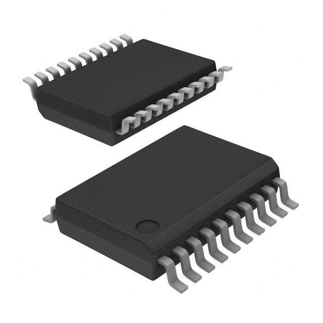
| 封装/箱体 | SOIC-8 |
| 工厂包装数量 | 97 |
| 最大工作温度 | + 70 C |
| 最大输出频率 | 1 GHz |
| 最小工作温度 | 0 C |
| 电源电压-最大 | 3.465 V |
| 电源电压-最小 | 2.375 V |
| 电源电流 | 25 mA |
| 系列 | 85311 |
| 输入类型 | Clock |
| 输出端数量 | 2 |
| 输出类型 | ECL, LVPECL |
| 零件号别名 | 85311 ICS85311AMLF |


- 商务部:美国ITC正式对集成电路等产品启动337调查
- 曝三星4nm工艺存在良率问题 高通将骁龙8 Gen1或转产台积电
- 太阳诱电将投资9.5亿元在常州建新厂生产MLCC 预计2023年完工
- 英特尔发布欧洲新工厂建设计划 深化IDM 2.0 战略
- 台积电先进制程称霸业界 有大客户加持明年业绩稳了
- 达到5530亿美元!SIA预计今年全球半导体销售额将创下新高
- 英特尔拟将自动驾驶子公司Mobileye上市 估值或超500亿美元
- 三星加码芯片和SET,合并消费电子和移动部门,撤换高东真等 CEO
- 三星电子宣布重大人事变动 还合并消费电子和移动部门
- 海关总署:前11个月进口集成电路产品价值2.52万亿元 增长14.8%


PDF Datasheet 数据手册内容提取
Low Skew, 1-to-2, Differential-to-2.5V, 3.3V 85311 LVPECL/ ECL Fanout Buffer Datasheet General Description Features The 85311 is a low skew, high performance 1-to-2 Differential-to- • Two differential 2.5V/3.3V LVPECL / ECL outputs 2.5V/3.3V ECL/LVPECL Fanout Buffer and a member of the high • One CLK, nCLK input pair performance clock solutions from IDT. The CLK, nCLK pair can accept most standard differential input levels. The 85311 is • CLK, nCLK pair can accept the following differential input levels: characterized to operate from either a 2.5V or a 3.3V power supply. LVDS, LVPECL, LVHSTL, SSTL, HCSL Guaranteed output and part-to-part skew characteristics make the 85311 ideal for those clock distribution applications demanding well • Maximum output frequency: 1GHz defined performance and repeatability. • Translates any single ended input signal to 3.3V LVPECL levels with resistor bias on nCLK input • Output skew: 15ps (maximum) • Part-to-part skew: 100ps (maximum) • Propagation delay: 1.4ns (maximum) • Additive phase jitter, RMS: 0.14ps (typical), 3.3V • LVPECL mode operating voltage supply range: V = 2.375V to 3.465V, V = 0V CC EE • ECL mode operating voltage supply range: V = 0V, V = -2.375V to -3.465V CC EE • 0°C to 70°C ambient operating temperature • Available in lead-free (RoHS 6) package Block Diagram Pin Assignment Q0 Q0 1 8 VCC CLKPulldown nQ0 nQ0 2 7 CLK nCLK Pullup Q1 Q1 3 6 nCLK nQ1 nQ1 4 5 VEE 85311 8-Lead SOIC 3.90mm x 4.903mm x 1.37mm package body M Package Top View ©2016 Integrated Device Technology, Inc. 1 Revision E, February 18, 2016
85311 Datasheet Pin Descriptions and Pin Characteristic Tables Table 1. Pin Descriptions Number Name Type Description 1, 2 Q0, nQ0 Output Differential output pair. LVPECL interface levels. 3, 4 Q1, nQ1 Output Differential output pair. LVPECL interface levels. 5 V Power Negative supply pin. EE 6 nCLK Input Pullup Inverting differential clock input. 7 CLK Input Pulldown Non-inverting differential clock input. 8 V Power Positive supply pin. CC NOTE: Pullup and Pulldown refer to internal input resistors. See Table 2, Pin Characteristics, for typical values. Table 2. Pin Characteristics Symbol Parameter Test Conditions Minimum Typical Maximum Units C Input Capacitance 4 pF IN R Input Pullup Resistor 51 k PULLUP R Input Pulldown Resistor 51 k PULLDOWN ©2016 Integrated Device Technology, Inc. 2 Revision E, February 18, 2016
85311 Datasheet Absolute Maximum Ratings NOTE: Stresses beyond those listed under Absolute Maximum Ratings may cause permanent damage to the device. These ratings are stress specifications only. Functional operation of product at these conditions or any conditions beyond those listed in the DC Characteristics or AC Characteristics is not implied. Exposure to absolute maximum rating conditions for extended periods may affect product reliability. Item Rating Supply Voltage, V 4.6V CC Inputs, V -0.5V to V + 0.5V I CC Outputs, I O Continuous Current 50mA Surge Current 100mA Storage Temperature, T -65C to 150C STG Package Thermal Impedance, 103C/W (0 lfpm) JA DC Electrical Characteristics Table 3A. Power Supply DC Characteristics, V = 3.3V±5% or 2.5V±5%, V = 0V, T = 0°C to 70°C CC EE A Symbol Parameter Test Conditions Minimum Typical Maximum Units 3.135 3.3 3.465 V V Positive Supply Voltage CC 2.375 2.5 2.625 V I Power Supply Current 25 mA EE Table 3B. Differential DC Characteristics, V = 3.3V±5% or 2.5V±5%, V = 0V, T = 0°C to 70°C CC EE A Symbol Parameter Test Conditions Minimum Typical Maximum Units nCLK V = V = 3.465V or 2.625V 5 µA CC IN I Input High Current IH CLK V = V = 3.465V or 2.625V 150 µA CC IN nCLK V = 3.465V or 2.625V, V = 0V -150 µA CC IN I Input Low Current IL CLK V = 3.465V or 2.625V, V = 0V -5 µA CC IN Peak-to-Peak Input Voltage; V 0.15 1.3 V PP NOTE 1 Common Mode Input Voltage; V V + 0.5 V – 0.85 V CMR NOTE 1, 2 EE CC NOTE 1: V should not be less than -0.3V. IL NOTE 2: Common mode voltage is defined as V . IH Table 3C. LVPECL DC Characteristics, V = 3.3V±5% or 2.5V±5%, V = 0V, T = 0°C to 70°C CC EE A Symbol Parameter Test Conditions Minimum Typical Maximum Units V Output High Current; NOTE 1 V – 1.4 V – 0.9 V OH CC CC V Output Low Current; NOTE 1 V – 2.0 V – 1.7 V OL CC CC V Peak-to-Peak Output Voltage Swing 0.65 1.0 V SWING NOTE1: Outputs terminated with 50 to V – 2V. CC ©2016 Integrated Device Technology, Inc. 3 Revision E, February 18, 2016
85311 Datasheet AC Electrical Characteristics Table 4A. AC Characteristics, V = 3.3V±5%, V = 0V, T = 0°C to 70°C CC EE A Symbol Parameter Test Conditions Minimum Typical Maximum Units f Maximum Output Frequency 1 GHz MAX t Propagation Delay; NOTE 1 ƒ 1GHz 0.9 1.4 ns PD Buffer Additive Phase Jitter, 156.25MHz, Integration Range tjit RMS; refer to Additive Phase 0.14 ps (12kHz – 20MHz) Jitter Section tsk(o) Output Skew; NOTE 2, 4 15 ps tsk(pp) Part-to-Part Skew; NOTE 3, 4 100 ps t / t Output Rise/Fall Time 20% to 80% @ 50MHz 300 700 ps R F odc Output Duty Cycle 48 52 % NOTE: Electrical parameters are guaranteed over the specified ambient operating temperature range, which is established when device is mounted in a test socket with maintained transverse airflow greater than 500 lfpm. Device will meet specifications after thermal equilibrium has been reached under these conditions. All parameters are measured 500MHz unless otherwise noted. NOTE 1: Measured from the differential input crossing point to the differential output crossing point. NOTE 2: Defined as skew between outputs at the same supply voltage and with equal load conditions. Measured at the differential cross points. NOTE 3: Defined as skew between outputs on different devices operating at the same supply voltages and with equal load conditions. Using the same type of inputs on each device, the outputs are measured at the differential cross points. NOTE 4: This parameter is defined in accordance with JEDEC Standard 65. Table 4B. AC Characteristics, V = 2.5V±5%, V = 0V, T = 0°C to 70°C CC EE A Symbol Parameter Test Conditions Minimum Typical Maximum Units f Maximum Output Frequency 1 GHz MAX t Propagation Delay; NOTE 1 ƒ 1GHz 0.9 1.4 ns PD Buffer Additive Phase Jitter, 156.25MHz, Integration Range tjit RMS; refer to Additive Phase 0.135 ps (12kHz – 20MHz) Jitter Section tsk(o) Output Skew; NOTE 2, 4 15 ps tsk(pp) Part-to-Part Skew; NOTE 3, 4 100 ps t / t Output Rise/Fall Time 20% to 80% @ 50MHz 300 700 ps R F odc Output Duty Cycle 48 52 % See Table 5A for NOTES. ©2016 Integrated Device Technology, Inc. 4 Revision E, February 18, 2016
85311 Datasheet Additive Phase Jitter (3.3V) The spectral purity in a band at a specific offset from the fundamental of the power in the 1Hz band to the power in the fundamental. When compared to the power of the fundamental is called the dBc Phase the required offset is specified, the phase noise is called a dBc value, Noise. This value is normally expressed using a Phase noise plot which simply means dBm at a specified offset from the fundamental. and is most often the specified plot in many applications. Phase noise By investigating jitter in the frequency domain, we get a better is defined as the ratio of the noise power present in a 1Hz band at a understanding of its effects on the desired application over the entire specified offset from the fundamental frequency to the power value of time record of the signal. It is mathematically possible to calculate an the fundamental. This ratio is expressed in decibels (dBm) or a ratio expected bit error rate given a phase noise plot. Additive Phase Jitter @ 156.25MH z 12kHz to 20MHz = 0.14ps (typical) z H c/ B d e s oi N e s a h P B S S Offset Frequency (Hz) As with most timing specifications, phase noise measurements has is illustrated above. The device meets the noise floor of what is issues relating to the limitations of the equipment. Often the noise shown, but can actually be lower. The phase noise is dependent on floor of the equipment is higher than the noise floor of the device. This the input source and measurement equipment. ©2016 Integrated Device Technology, Inc. 5 Revision E, February 18, 2016
85311 Datasheet Parameter Measurement Information 2V 2V SCOPE SCOPE VCC Qx VCC Qx nQx nQx VEE VEE -1.3V ± 0.165V -0.5V ± 0.125V 3.3V Core/ 3.3V LVPECL Output Load AC Test Circuit 2.5V Core/ 2.5V LVPECL Output Load AC Test Circuit VCC nQx Qx nCLK V Cross Points V nQy PP CMR CLK Qy VEE Differential Input Level Output Skew Part 1 nQx nCLK Qx CLK nQy Part 2 nQ[0:1] Qy Q[0:1] tsk(pp) tPD Part-to-Part Skew Propagation Delay ©2016 Integrated Device Technology, Inc. 6 Revision E, February 18, 2016
85311 Datasheet Parameter Measurement Information, continued nQ[0:1] nQ[0:1] Q[0:1] Q[0:1] Output Duty Cycle/Pulse Width/Period Output Rise/Fall Time Applications Information Wiring the Differential Input to Accept Single Ended Levels Figure 1 shows how the differential input can be wired to accept single ended levels. The reference voltage V_REF = V /2 is generated by the bias resistors R1, R2 and C1. This biaCsC circuit VCC should be located as close as possible to the input pin. The ratio of R1 and R2 might need to be adjusted to position the V_REF in the center of the input voltage swing. For example, if the input clock R1 1K swing is only 2.5V and V = 3.3V, V_REF should be 1.25V and CC R2/R1 = 0.609. Single Ended Clock Input CLK V_REF nCLK C1 0.1u R2 1K Figure 1. Single-Ended Signal Driving Differential Input ©2016 Integrated Device Technology, Inc. 7 Revision E, February 18, 2016
85311 Datasheet Differential Clock Input Interface The CLK /nCLK accepts LVDS, LVPECL, LVHSTL, SSTL, HCSL only. Please consult with the vendor of the driver component to and other differential signals. Both signals must meet the V and confirm the driver termination requirements. For example, in Figure PP V input requirements. Figures 2A to 2F show interface 2A, the input termination applies for IDT’s open emitter LVHSTL CMR examples for the CLK/nCLK input driven by the most common drivers. If you are using an LVHSTL driver from another vendor, driver types. The input interfaces suggested here are examples use their termination recommendation. 3.3V 1.8V Zo = 50Ω CLK Zo = 50Ω nCLK LVHSTL Differential Input ILDVTHSTL Driver R501Ω R502Ω Figure 2A. CLK/nCLK Input Driven by an Figure 2B. CLK/nCLK Input Driven by a IDT Open Emitter LVHSTL Driver 3.3V LVPECL Driver Figure 2C. CLK/nCLK Input Driven by a 3.3V LVPECL Driver Figure 2D. CLK/nCLK Input Driven by a 3.3V LVDS Driver 3.3V 3.3V 2.5V 3.3V *R3 2.5V R1230Ω R1240Ω CLK Zo = 60Ω CLK nCLK Zo = 60Ω HCSL *R4 DInipffuetrential nCLK Differential SSTL Input R1 R2 120Ω 120Ω Figure 2E. CLK/nCLK Input Driven by a 3.3V HCSL Driver Figure 2F. CLK/nCLK Input Driven by a 2.5V SSTL Driver ©2016 Integrated Device Technology, Inc. 8 Revision E, February 18, 2016
85311 Datasheet Recommendations for Unused Output Pins Outputs: LVPECL Outputs All unused LVPECL outputs can be left floating. We recommend that there is no trace attached. Both sides of the differential output pair should either be left floating or terminated. Termination for 3.3V LVPECL Outputs The clock layout topology shown below is a typical termination for transmission lines. Matched impedance techniques should be LVPECL outputs. The two different layouts mentioned are used to maximize operating frequency and minimize signal recommended only as guidelines. distortion. Figures 3A and 3B show two different layouts which are recommended only as guidelines. Other suitable clock layouts may FOUT and nFOUT are low impedance follower outputs that exist and it would be recommended that the board designers generate ECL/LVPECL compatible outputs. Therefore, terminating simulate to guarantee compatibility across all printed circuit and resistors (DC current path to ground) or current sources must be clock component process variations. used for functionality. These outputs are designed to drive 50 3.3V R3 R4 125 125 3.3V 3.3V Z = 50 o + _ Input Z = 50 o R1 R2 84 84 Figure 3A. 3.3V LVPECL Output Termination Figure 3B. 3.3V LVPECL Output Termination ©2016 Integrated Device Technology, Inc. 9 Revision E, February 18, 2016
85311 Datasheet Termination for 2.5V LVPECL Outputs Figure 4A and Figure 4B show examples of termination for 2.5V level. The R3 in Figure 4B can be eliminated and the termination is LVPECL driver. These terminations are equivalent to terminating 50 shown in Figure 4C. to V – 2V. For V = 2.5V, the V – 2V is very close to ground CC CC CC 2.5V VCC = 2.5V 2.5V 2.5V VCC = 2.5V R1 R3 50Ω 250Ω 250Ω + 50Ω + 50Ω – 50Ω 2.5V LVPECL Driver – R1 R2 50Ω 50Ω 2.5V LVPECL Driver R2 R4 62.5Ω 62.5Ω R3 18Ω Figure 4A. 2.5V LVPECL Driver Termination Example Figure 4B. 2.5V LVPECL Driver Termination Example 2.5V VCC = 2.5V 50Ω + 50Ω – 2.5V LVPECL Driver R1 R2 50Ω 50Ω Figure 4C. 2.5V LVPECL Driver Termination Example ©2016 Integrated Device Technology, Inc. 10 Revision E, February 18, 2016
85311 Datasheet Power Considerations This section provides information on power dissipation and junction temperature for the 85311. Equations and example calculations are also provided. 1. Power Dissipation. The total power dissipation for the 85311 is the sum of the core power plus the power dissipated in the load(s). The following is the power dissipation for V = 3.3V + 5% = 3.465V, which gives worst case results. CC NOTE: Please refer to Section 3 for details on calculating power dissipated in the load. (cid:129) Power (core) = V * I = 3.465V * 25mA = 86.6mW MAX CC_MAX EE_MAX (cid:129) Power (outputs) = 30mW/Loaded Output pair MAX If all outputs are loaded, the total power is 2 * 30mW = 60mW Total Power_ (3.3V, with all outputs switching) = 86.6mW + 60mW = 146.6mW MAX 2. Junction Temperature. Junction temperature, Tj, is the temperature at the junction of the bond wire and bond pad and directly affects the reliability of the device. The maximum recommended junction temperature for devices is 125°C. The equation for Tj is as follows: Tj = * Pd_total + T JA A Tj = Junction Temperature = Junction-to-Ambient Thermal Resistance JA Pd_total = Total Device Power Dissipation (example calculation is in section 1 above) T = Ambient Temperature A In order to calculate junction temperature, the appropriate junction-to-ambient thermal resistance must be used. Assuming no air flow JA and a multi-layer board, the appropriate value is 103°C/W per Table 5 below. Therefore, Tj for an ambient temperature of 70°C with all outputs switching is: 70°C + 0.147W * 103°C/W = 85.14°C. This is well below the limit of 125°C. This calculation is only an example. Tj will obviously vary depending on the number of loaded outputs, supply voltage, air flow and the type of board (single layer or multi-layer). Table 5. Thermal Resistance for 8 Lead SOIC, Forced Convection JA vs. Air Flow JA Linear Feet per Minute 0 200 500 Multi-Layer PCB, JEDEC Standard Test Boards 103°C/W 94°C/W 89°C/W ©2016 Integrated Device Technology, Inc. 11 Revision E, February 18, 2016
85311 Datasheet 3. Calculations and Equations. The purpose of this section is to derive the power dissipated into the load. LVPECL output driver circuit and termination are shown in Figure 5. V CC Q1 V OUT RL V -2V CC Figure 5. LVPECL Driver Circuit and Termination To calculate worst case power dissipation into the load, use the following equations which assume a 50 load, and a termination voltage of V – 2V. CC (cid:129) For logic high, V = V = V – 0.9V OUT OH_MAX CC_MAX (V – V ) = 0.9V CC_MAX OH_MAX (cid:129) For logic low, V = V = V – 1.7V OUT OL_MAX CC_MAX (V – V ) = 1.7V CC_MAX OL_MAX Pd_H is power dissipation when the output drives high. Pd_L is the power dissipation when the output drives low. Pd_H = [(V (V – 2V))/R ] * (V – V ) = [(2V – (V – V ))/R ] * (V – V ) = OH_MAX – CC_MAX L CC_MAX OH_MAX CC_MAX OH_MAX L CC_MAX OH_MAX [(2V – 0.9V)/50] * 0.9V = 19.8mW Pd_L = [(V – (V – 2V))/R ] * (V – V ) = [(2V – (V – V ))/R ] * (V – V ) = OL_MAX CC_MAX L CC_MAX OL_MAX CC_MAX OL_MAX L CC_MAX OL_MAX [(2V – 1.7V)/50] * 1.7V = 10.2mW Total Power Dissipation per output pair = Pd_H + Pd_L = 30mW ©2016 Integrated Device Technology, Inc. 12 Revision E, February 18, 2016
85311 Datasheet Reliability Information Table 6. vs. Air Flow Table for a 8 Lead SOIC JA by Velocity JA Linear Feet per Minute 0 200 500 Multi-Layer PCB, JEDEC Standard Test Boards 103°C/W 94°C/W 89°C/W Transistor Count The transistor count for 85311 is: 225 Package Outline and Package Dimensions Package Outline - M Suffix for 8 Lead SOIC Table 7. Package Dimensions All Dimensions in Millimeters Symbol Minimum Maximum N 8 A 1.35 1.75 A1 0.10 0.25 B 0.33 0.51 C 0.19 0.25 D 4.80 5.00 E 3.80 4.00 e 1.27 Basic H 5.80 6.20 h 0.25 0.50 L 0.40 1.27 0° 8° Reference Document: JEDEC Publication 95, MS-012 150 il (N B d ) SOIC ©2016 Integrated Device Technology, Inc. 13 Revision E, February 18, 2016
85311 Datasheet Ordering Information Table 8. Ordering Information Part/Order Number Marking Package Shipping Packaging Temperature 85311AMLF 85311ALF “Lead-Free” 8 Lead SOIC Tube 0C to 70C 85311AMLFT 85311ALF “Lead-Free” 8 Lead SOIC Tape & Reel 0C to 70C ©2016 Integrated Device Technology, Inc. 14 Revision E, February 18, 2016
85311 Datasheet Revision History Sheet Rev Table Page Description of Change Date A 8 Added Termination for LVPECL Outputs section. 5/30/02 5 3.3V Output Load Test Circuit Diagram - corrected VEE equation to read A -1.3V ± 0.165V from ± 0.135V. 9/23/02 7 Updated Output Rise/Fall Time Diagram. 1 Add Lead-Free bullet in Features section. T2 2 Pin Characteristics table - changed C 4pF max. to 4pF typical. IN 3 Absolute Maximum Ratings, updated Outputs rating. 3 Combined 3.3V & 2.5V Power tables and Differential DC Characteristics tables. B 5 Updated Parameter Measurement Information. 6/17/04 6 Updated Single Ended Signal Driving Differential Input diagram. 7 Added Termination for 2.5V LVPECL Output section. T8 8 Added Differential Clock Input Interface section. 13 Ordering Information table - added Lead Free part number. 7 Added Recommendations for Unused Input and Output Pins. B T8 13 Ordering Information Table - corrected Lead-Free marking and added 7/28/05 Lead-Free Note. T3 3 LVPECL DC Characteristics Table -corrected V max. from V - 1.0V to V - OH CC CCO C 0.9V; and V max. from 0.9V to 1.0V. 4/11/07 SWING 9 - 10 Power Considerations - corrected power dissipation to reflect VOH max in Table 3C. T4A - T4B 4 Added 2.5V AC Characteristics Table. Added Additive Phase Jitter spec to both AC Tables. D 10/22/08 5 Added Additive Phase Jitter plot. 8 Updated Differential Input Clock Interface section. T8 14 Ordering Information - removed leaded devices. D 7/8/15 Updated data sheet format. 11 Power Considerations - updated Junction Temperature section and corrected Table 5, Thermal Resistance Table. T6 13 Corrected table. E T8 14 2/16/16 Ordering Information Table - deleted table note. Deleted HiperClockS reference throughout the datasheet. Updated datasheet header/footer. ©2016 Integrated Device Technology, Inc. 15 Revision E, February 18, 2016
Corporate Headquarters Sales Tech Support 6024 Silver Creek Valley Road 1-800-345-7015 or 408-284-8200 email: clocks@idt.com San Jose, CA 95138 USA Fax: 408-284-2775 www.IDT.com DISCLAIMER Integrated Device Technology, Inc. (IDT) and its subsidiaries reserve the right to modify the products and/or specifications described herein at any time and at IDT’s sole discretion. All information in this document, including descriptions of product features and performance, is subject to change without notice. Performance specifications and the operating parameters of the described products are determined in the independent state and are not guaranteed to perform the same way when installed in customer products. The information contained herein is provided without representation or warranty of any kind, whether express or implied, including, but not limited to, the suitability of IDT’s products for any particular purpose, an implied warranty of merchantability, or non-infringement of the intellectual property rights of others. Thi s document is presented only as a guide and does not convey any license under intellectual property rights of IDT or any third parties. IDT’s products are not intended for use in applications involving extreme environmental conditions or in life support systems or similar devices where the failure or malfunction of an IDT product can be reasonabl y expected to significantly affect the health or safety of users. Anyone using an IDT product in such a manner does so at their own risk, absent an express, written agreement by IDT. While the information presented herein has been checked for both accuracy and reliability, Integrated Device Technology (IDT) assumes no responsibility for either its use or for the infringement of any patents o r other rights of third parties, which would result from its use. No other circuits, patents, or licenses are implied. This product is intended for use in normal commercial applications. Any other applications, such a s those requiring extended temperature ranges, high reliability or other extraordinary environmental requirements are not recommended without additional processing by IDT. IDT reserves the right to change any circuitry or specifications without notice. IDT does not authorize or warrant any IDT product for use in life support devices or critical medical instruments. Integrated Device Technology, IDT and the IDT logo are registered trademarks of IDT. Product specification subject to change without notice. Other trademarks and service marks used herein, including protected names, logos and designs, are the property of IDT or their respective third party owners. Copyright ©2015 Integrated Device Technology, Inc. All rights reserved.
Mouser Electronics Authorized Distributor Click to View Pricing, Inventory, Delivery & Lifecycle Information: I DT (Integrated Device Technology): 85311AMLF 85311AMLFT