ICGOO在线商城 > 集成电路(IC) > 时钟/计时 - 时钟发生器,PLL,频率合成器 > 843001AG-21LF

 Datasheet下载
- 型号: 843001AG-21LF
- 制造商: Integrated Device Technology
- 库位|库存: xxxx|xxxx
- 要求:
| 数量阶梯 | 香港交货 | 国内含税 |
| +xxxx | $xxxx | ¥xxxx |
查看当月历史价格
查看今年历史价格
843001AG-21LF产品简介:
ICGOO电子元器件商城为您提供843001AG-21LF由Integrated Device Technology设计生产,在icgoo商城现货销售,并且可以通过原厂、代理商等渠道进行代购。 843001AG-21LF价格参考。Integrated Device Technology843001AG-21LF封装/规格:时钟/计时 - 时钟发生器,PLL,频率合成器, 。您可以下载843001AG-21LF参考资料、Datasheet数据手册功能说明书,资料中有843001AG-21LF 详细功能的应用电路图电压和使用方法及教程。
| 参数 | 数值 |
| 品牌 | IDT |
| 产品目录 | 半导体 |
| 描述 | 时钟合成器/抖动清除器 1 LVPECL/1 LVCMOS REF OUT |
| 产品分类 | 集成电路 - IC |
| 产品手册 | http://www.idt.com/document/dst/843001-21-datasheet |
| 产品图片 |
|
| rohs | 符合RoHS |
| 产品系列 | 时钟和计时器IC,时钟合成器/抖动清除器,IDT 843001AG-21LF |
| 产品型号 | 843001AG-21LF |
| 产品种类 | 时钟合成器/抖动清除器 |
| 商标 | IDT |
| 安装风格 | SMD/SMT |
| 封装 | Tube |
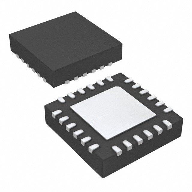
| 封装/箱体 | TSSOP-24 |
| 工厂包装数量 | 62 |
| 最大工作温度 | + 70 C |
| 最大输入频率 | 40 MHz |
| 最大输出频率 | 700 MHz |
| 最小工作温度 | 0 C |
| 电源电压-最大 | 3.465 V |
| 电源电压-最小 | 3.135 V |
| 电源电流 | 170 mA |
| 系列 | 843001-21 |
| 输入电平 | Crystal, LVCMOS, LVTTL |
| 输出电平 | LVCMOS, LVTTL, LVPECL |
| 输出端数量 | 2 |
| 零件号别名 | 843001-21 ICS843001AG-21LF |


- 商务部:美国ITC正式对集成电路等产品启动337调查
- 曝三星4nm工艺存在良率问题 高通将骁龙8 Gen1或转产台积电
- 太阳诱电将投资9.5亿元在常州建新厂生产MLCC 预计2023年完工
- 英特尔发布欧洲新工厂建设计划 深化IDM 2.0 战略
- 台积电先进制程称霸业界 有大客户加持明年业绩稳了
- 达到5530亿美元!SIA预计今年全球半导体销售额将创下新高
- 英特尔拟将自动驾驶子公司Mobileye上市 估值或超500亿美元
- 三星加码芯片和SET,合并消费电子和移动部门,撤换高东真等 CEO
- 三星电子宣布重大人事变动 还合并消费电子和移动部门
- 海关总署:前11个月进口集成电路产品价值2.52万亿元 增长14.8%


PDF Datasheet 数据手册内容提取
FemtoClocks™ Crystal-to-3.3V LVPECL 843001-21 Frequency Synthesizer PRODUCT DISCONTINUATION NOTICE - LAST TIME BUY EXPIRES MAY 6, 2017 DATA SHEET Description Features The 843001-21 is a a highly versatile, low phase noise LVPECL • One 3.3Vdifferential LVPECL output pair and Synthesizer which can generate low jitter reference clocks for a one LVCMOS/LVTTL single-ended reference clock output variety of communications applications. The dual crystal interface • Selectable crystal oscillator interface allows the synthesizer to support up to two communications or LVCMOS/LVTTL single-ended input standards in a given application (i.e. 1GB Ethernet with a 25MHz • VCO range: 560MHz – 700MHz crystal and 1Gb Fibre Channel using a 26.5625MHz crystal). The • Supports the following applications: rms phase jitter performance is typically less than 1ps, thus SONET, Ethernet, Fibre Channel, Serial ATA, and HDTV making the device acceptable for use in demanding applications • Selectable ÷1 or ÷2 operation such as OC48 SONET and 10Gb Ethernet. The 843001-21 is packaged in a small 24-pin TSSOP package. • RMS phase jitter @ 622.08MHz (12kHz - 20MHz): 0.80ps (typical) Offset Noise Power 100Hz................-60.3 dBc/Hz 1kHz..................-88.5 dBc/Hz 10kHz................-111.9 dBc/Hz 100kHz..............-113.0 dBc/Hz • Full 3.3V supply mode • 0°C to 70°C ambient operating temperature • Available in lead-free (RoHS 6) package • For drop in replacement use 843001i-22 Pin Assignment Block Diagram VCCO_CMOS 1 24 REF_CLK 3 N0 2 23 VEE N2:N0 N1 3 22 OE_REF N2 4 21 M2 SEL0 Pulldown VCCO_PECL 5 20 M1 Q0 6 19 M0 SEL1 Pulldown Q0 7 18 MR N VEE 8 17 SEL1 VCCA 9 16 SEL0 XTAL_IN0 000 ÷1 VCC 10 15 TEST_CLK OSC 00 11 001 ÷2 XTAL_OUT1 11 14 XTAL_IN0 010 ÷3 Q0XTAL_IN1 12 13 XTAL_OUT0 XTAL_OUT0 011 ÷4 (default) Phase 10 100 ÷5 Q0 843001-21 XTAL_IN1 OSC 01 Detector VCO 0010 110110 ÷÷68 24-Lead TSSOP 4.4mm x 7.8mm x 0.925mm XTAL_OUT1 111 ÷10 package body M TEST_CLK Pulldown 10 000 ÷18 G Package 001 ÷22 Top View 010 ÷24 011 ÷25 100 ÷32 (default) 101 ÷40 MR Pulldown 3 M2:M0 REF_CLK OE_REF Pulldown 843001-21 Rev A 5/20/16 1 ©2016 Integrated Device Technology, Inc.
843001-21 DATA SHEET Table 1. Pin Descriptions Number Name Type Description 1 V Power Output supply pin for REF_CLK output. CCO_CMOS 2, 3 N0, N1 Input Pullup Output divider select pins. Default ÷4. LVCMOS/LVTTL interface levels. 4 N2 Input Pulldown See Table 3C. 5 V Power Output supply pin for LVPECL output. CCO_PECL 6, 7 Q0, Q0 Output Differential output pair. LVPECL interface levels. 8, 23 V Power Negative supply pins. EE 9 V Power Analog supply pin. CCA 10 V Power Core supply pin. CC 11, XTAL_OUT1, Parallel resonant crystal interface. Input 12 XTAL_IN1 XTAL_OUT1 is the output, XTAL_IN1 is the input. 13, XTAL_OUT0, Parallel resonant crystal interface. Input 14 XTAL_IN0 XTAL_OUT0 is the output, XTAL_IN0 is the input. 15 TEST_CLK Input Pulldown LVCMOS/LVTTL clock input. 16, 17 SEL0, SEL1 Input Pulldownp Input MUX select pins. LVCMOS/LVTTL interface levels. See Table 3D. Active HIGH Master Reset. When logic HIGH, the internal dividers are reset causing the true output Q0 to go low and the inverted output Q0 to go high. 18 MR Input Pulldown When logic LOW, the internal dividers and the outputs are enabled. LVCMOS/LVTTL interface levels. 19, 20 M0, M1 Input Pulldown Feedback divider select pins. Default ÷32. See Table 3B 21 M2 Input Pullup LVCMOS/LVTTL interface levels. 22 OE_REF Input Pulldown Reference clock output enable. Default Low. LVCMOS/LVTTL interface levels. 24 REF_CLK Output Reference clock output. LVCMOS/LVTTL interface levels. NOTE: Pullup and Pulldown refer to intenal input resistors. See Table 2, Pin Characteristics, for typical values. Table 2. Pin Characteristics Symbol Parameter Test Conditions Minimum Typical Maximum Units C Input Capacitance 4 pF IN R Input Pullup Resistor 51 k PULLUP R Input Pulldown Resistor 51 k PULLDOWN R Output Impedance 7 OUT Rev A 5/20/16 2 FEMTOCLOCKS™ CRYSTAL-TO-3.3V LVPECL FREQUENCY SYNTHESIZER
843001-21 DATA SHEET Function Tables Table 3A. Common Configuration Table Input M Divider N Divider Output Frequency Reference Clock (MHz) Value Value VCO (MHz) (MHz) Application 27 22 8 594 74.25 HDTV 24.75 24 8 594 74.25 HDTV 14.8351649 40 8 593.4066 74.1758245 HDTV 19.44 32 4 622.08 155.52 SONET 19.44 32 8 622.08 77.76 SONET 19.44 32 1 622.08 622.08 SONET 19.44 32 2 622.08 311.04 SONET 19.53125 32 4 625 156.25 10 GigE 25 25 5 625 125 1 GigE 25 25 10 625 62.5 1 GigE 25 24 6 600 100 PCI Express 25 24 4 600 150 SATA 25 24 8 600 75 SATA 26.5625 24 6 637.5 106.25 Fibre Channel 1 26.5625 24 3 637.5 212.5 4 Gig Fibre Channel 26.5625 24 4 637.5 159.375 10 Gig Fibre Channel 31.25 18 5 562.5 187.5 12 GigE Table 3B. Programmable M Output Divider Function Table Inputs Input Frequency (MHz) M Divider M2 M1 M0 Value Minimum Maximum 0 0 0 18 31.1 38.9 0 0 1 22 25.5 31.8 0 1 0 24 23.3 29.2 0 1 1 25 22.4 28.0 1 0 0 32 17.5 21.9 1 0 1 40 14.0 17.5 Table 3C. Programmable N Output Divider Inputs Function Table M Divider N2 N1 N0 Value Inputs M Divider 0 1 1 4 N2 N1 N0 Value 1 0 0 5 0 0 0 1 0 0 1 2 0 1 0 3 FEMTOCLOCKS™ CRYSTAL-TO-3.3V LVPECL FREQUENCY 3 Rev A 5/20/16 SYNTHESIZER
843001-21 DATA SHEET Inputs M Divider N2 N1 N0 Value 1 0 1 6 1 1 0 8 1 1 1 10 Table 3D. Bypass Mode Function Table Inputs SEL1 SEL0 Reference PLL Mode 0 0 XTAL0 1 0 1 XTAL1 2 1 0 TEST_CLK 8 1 1 TEST_CLK1 10 Rev A 5/20/16 4 FEMTOCLOCKS™ CRYSTAL-TO-3.3V LVPECL FREQUENCY SYNTHESIZER
843001-21 DATA SHEET Absolute Maximum Ratings NOTE: Stresses beyond those listed under Absolute Maximum Ratings may cause permanent damage to the device. These ratings are stress specifications only. Functional operation of product at these conditions or any conditions beyond those listed in the DC Characteristics or AC Characterisitcs is not implied. Exposure to absolute maximum rating conditions for extended periods may affect product reliability. Item Rating Supply Voltage, V 4.6V CC Inputs, V -0.5V to V + 0.5V I CC Outputs, I (LVPECL) O Continuous Current 50mA Surge Current 100mA Outputs, V (LVCMOS) -0.5V to V + 0.5V O CCO_CMOS Package Thermal Impedance, 70C/W (0 mps) JA Storage Temperature, T -65C to 150C STG DC Electrical Characteristics Table 4A. Power Supply DC Characteristics, V = V = V = V = 3.3V ± 5%, T = 0°C to 70°C CC CCA CCO_CMOS CCO_PECL A Symbol Parameter Test Conditions Minimum Typical Maximum Units V Core Supply Voltage 3.135 3.3 3.465 V CC V Analog Supply Voltage 3.135 3.3 3.465 V CCA V CCO_PECL, Output Supply Voltage 3.135 3.3 3.465 V V CCO_CMOS I Power Supply Current 170 mA EE I Analog Supply Current 11 mA CCA I CCO_PECL, Output Supply Current 8 mA I CCO_CMOS FEMTOCLOCKS™ CRYSTAL-TO-3.3V LVPECL FREQUENCY 5 Rev A 5/20/16 SYNTHESIZER
843001-21 DATA SHEET Table 4B. LVCMOS/LVTTL DC Characteristics, V = V = V = 3.3V ± 5%, T = 0°C to 70°C CC CCA CCO_CMOS A Symbol Parameter Test Conditions Minimum Typical Maximum Units V Input High Voltage 2 V + 0.3 V IH CC SEL0, SEL1, OE_REF, -0.3 0.8 V V Input Low Voltage N0:N2, MR, M0:M2 IL TEST_CLK -0.3 1.3 V TEST_CLK, M0, M1, N2, MR, OE_REF, V = V = 3.465V 150 µA CC IN IIH Input High Current SEL0, SEL1 M2, N0, N1 V = V = 3.465V 5 µA CC IN TEST_CLK, M0, M1, V = 3.465V, N2, MR, OE_REF, CC -5 µA V = 0V I Input Low Current SEL0, SEL1 IN IL V = 3.465V, M2, N0, N1 CC -150 µA V = 0V IN Output High Voltage: V REF_CLK 2.6 V OH NOTE 1 Output Low Voltage: V REF_CLK 0.5 V OL NOTE 1 NOTE 1: Output terminated with 50 to V /2. See Parameter Measurement Information Section, CCO _CMOS ""3.3V LVCMOS Output Load Test Circuit Diagram"". Table 4C. LVPECL DC Characteristics, V = V = V = 3.3V ± 5%, T = 0°C to 70°C CC CCA CCO_PECL A Symbol Parameter Test Conditions Minimum Typical Maximum Units V Output High Current; NOTE 1 V – 1.4 V – 0.9 µA OH CCO CCO V Output Low Current; NOTE 1 V – 2.0 V – 1.7 µA OL CCO CCO V Peak-toPeak Output Voltage Swing 0.6 1.0 V SWING NOTE 1: Outputs termination with 50 to V – 2V. CCO_PECL Table 5. Crystal Characteristics Parameter Test Conditions Minimum Typical Maximum Units Mode of Oscillation Fundamental Frequency 12 40 MHz Equivalent Series Resistance (ESR) 50 Shunt Capacitance 7 pF NOTE: Characterized using an 18pF parallel resonant crystal. Rev A 5/20/16 6 FEMTOCLOCKS™ CRYSTAL-TO-3.3V LVPECL FREQUENCY SYNTHESIZER
843001-21 DATA SHEET AC Electrical Characteristics Table 6. AC Characteristics, V = V = V = V = 3.3V ± 5%, T = 0°C to 70°C CC CCA CCO_CMOS CCO_PECL A Parameter Symbol Test Conditions Minimum Typical Maximum Units f Output Frequency 56 700 MHz OUT Propagation Delay; TEST_CLK to t 2.3 2.8 ns PD NOTE 1 REF_CLK RMS Phase Jitter, (Random); 622.08MHz, tjit(Ø) 0.80 ps NOTE 2, 3 (12kHz – 20MHz) t PLL VCO Lock Range 560 700 MHz VCO Output Q0, Q0 20% to 80% 200 500 ps t / t R F Rise/Fall Time REF_CLK 20% to 80% 300 800 ps Q0, Q0 45 55 % odc Output Duty Cycle REF_CLK 44 56 % NOTE 1: Measured from the V /2 of the input to V /2 of the output. CC CCO_CMOS NOTE 2: Phase jitter measured using a 19.44MHz quartz crystal. NOTE 3: This parameter is defined in accordance with JEDEC Standard 65. Typical Phase Noise at 622.08MHz 0 -10 ➝ OC-12 Filter -20 -30 622.08MHz RMS Phase Jitter (Random) -40 12kHz to 20MHz = 0.80ps (typical) -50 -60 BcHz -70 d -80 r e w -90 o ➝ Raw Phase Noise Data P -100 e s oi -110 N -120 ➝ -130 Phase Noise Result by adding a -140 Sonet OC-12 filter to raw data -150 -160 -170 -180 -190 100 1k 10k 100k 1M 10M 100M Offset Frequency (Hz) FEMTOCLOCKS™ CRYSTAL-TO-3.3V LVPECL FREQUENCY 7 Rev A 5/20/16 SYNTHESIZER
843001-21 DATA SHEET Parameter Measurement Information 2V% 1.65V±5% SCOPE SCOPE VCC, Qx VCC, VCCA, VCCA, VCCO_PECL VCCO_CMOS Qx nQx GND V EE -1.65V±5% -1.3V ± 0.165V - 3.3V LVPECL Output Load AC Test Circuit 3.3V LVCMOS Output Load AC Test Circuit Phase Noise Plot V er CC w TEST_CLK 2 o P e s oi Phase Noise Mask N V CCO_LVCMOS REF_CLK 2 t Offset Frequency PD f f 1 2 RMS Jitter = Area Under the Masked Phase Noise Plot RMS Phase Jitter Propagation Delay Q0 V CCO_CMOS 2 Q0 REF_CLK t PW t PERIOD t PW odc = x 100% t PERIOD LVPECL Output Duty Cycle/Pulse Width/Period LVCMOS Output Duty Cycle/Pulse Width/Period Rev A 5/20/16 8 FEMTOCLOCKS™ CRYSTAL-TO-3.3V LVPECL FREQUENCY SYNTHESIZER
843001-21 DATA SHEET Parameter Measurement Information, continued 80% 80% 80% 80% V SWING Clock 20% 20% 20% 20% Outputs Clock tR tF Outputs tR tF LVPECL Output Rise/Fall Time LVCMOS Output Rise/Fall Time Application Information Power Supply Filtering Technique As in any high speed analog circuitry, the power supply pins are vulnerable to random noise. The 843001-21 provides separate power supplies to isolate any high switching noise from the outputs 3.3V to the internal PLL. VCC, VCCA and VCCO_x should be individually VCC connected to the power supply plane through vias, and bypass 0.01µF capacitors should be used for each pin. To achieve optimum jitter performance, power supply isolation is required. Figure 1 VCCA illustrates how a 10 resistor along with a 10F and a .01F 0.01µF 10µF bypass capacitor should be connected to each V pin. CCA Figure 1. Power Supply Filtering FEMTOCLOCKS™ CRYSTAL-TO-3.3V LVPECL FREQUENCY 9 Rev A 5/20/16 SYNTHESIZER
843001-21 DATA SHEET Crystal Input Interface The 843001-21 has been characterized with 18pF parallel were determined using a 19.44MHz, 18pF parallel resonant crystal resonant crystals. The capacitor values shown in Figure 2 below and were chosen to minimize the ppm error. XTAL_IN C1 22pF X1 18pF Parallel Crystal XTAL_OUT C2 22pF Figure 2. Crystal Input Interface LVCMOS to XTAL Interface The XTAL_IN input can accept a single-ended LVCMOS signal impedance of the driver (Ro) plus the series resistance (Rs) equals through an AC coupling capacitor. A general interface diagram is the transmission line impedance. In addition, matched termination shown in Figure 3. The XTAL_OUT pin can be left floating. The at the crystal input will attenuate the signal in half. This can be input edge rate can be as slow as 10ns. For LVCMOS inputs, it is done in one of two ways. First, R1 and R2 in parallel should equal recommended that the amplitude be reduced from full swing to half the transmission line impedance. For most 50 applications, R1 swing in order to prevent signal interference with the power rail and and R2 can be 100. This can also be accomplished by removing to reduce noise. This configuration requires that the output R1 and making R2 50. VCC VCC R1 Ro Rs 50Ω 0.1µf XTAL_IN Zo = Ro + Rs R2 XTAL_OUT Figure 3. General Disgram for LVCMOS Driver to XTAL Input Interface Rev A 5/20/16 10 FEMTOCLOCKS™ CRYSTAL-TO-3.3V LVPECL FREQUENCY SYNTHESIZER
843001-21 DATA SHEET Recommendations for Unused Input and Output Pins Inputs: Outputs: Crystal Inputs: LVPECL Output: For applications not requiring the use of the crystal oscillator input, All unused LVPECL outputs can be left floating. We recommend both XTAL_IN and XTAL_OUT can be left floating. Though not that there is no trace attached. Both sides of the differential output required, but for additional protection, a 1k resistor can be tied pair should either be left floating or terminated. from XTAL_IN to ground. LVCMOS Output: TEST_CLK Input: All unused LVCMOS output can be left floating. We recommend For applications not requiring the use of the test clock, it can be left that there is no trace attached. floating. Though not required, but for additional protection, a 1k resistor can be tied from the TEST_CLK to ground. LVCMOS Control Pins: All control pins have internal pull-ups or pull-downs; additional resistance is not required but can be added for additional protection. A 1k resistor can be used. Termination for 3.3V LVPECL Outputs The clock layout topology shown below is a typical termination for transmission lines. Matched impedance techniques should be LVPECL outputs. The two different layouts mentioned are used to maximize operating frequency and minimize signal recommended only as guidelines. distortion. Figures 4A and 4B show two different layouts which are recommended only as guidelines. Other suitable clock layouts may FOUT and FOUT are low impedance follower outputs that exist and it would be recommended that the board designers generate ECL/LVPECL compatible outputs. Therefore, terminating simulate to guarantee compatibility across all printed circuit and resistors (DC current path to ground) or current sources must be clock component process variations. used for functionality. These outputs are designed to drive 50 3.3V Z = 50Ω o 125Ω 125Ω FOUT FIN Z = 50Ω o Z = 50Ω o FOUT FIN 50Ω 50Ω VCC - 2V Zo = 50Ω 1 RTT = Z RTT ((VOH + VOL) / (VCC – 2)) – 2 o 84Ω 84Ω Figure 4A. 3.3V LVPECL Output Termination Figure 4B. 3.3V LVPECL Output Termination FEMTOCLOCKS™ CRYSTAL-TO-3.3V LVPECL FREQUENCY 11 Rev A 5/20/16 SYNTHESIZER
843001-21 DATA SHEET Power Considerations This section provides information on power dissipation and junction temperature for the ICS843001.21. Equations and example calculations are also provided. 1. Power Dissipation. The total power dissipation for the 843001-21 is the sum of the core power plus the power dissipated in the load(s). The following is the power dissipation for V = 3.3V + 5% = 3.465V, which gives worst case results. CC NOTE: Please refer to Section 3 for details on calculating power dissipated in the load. (cid:129) Power (core) = V * I = 3.465V * 170mA = 589.05mW MAX CC_MAX EE_MAX (cid:129) Power (outputs) = 30mW/Loaded Output pair MAX Total Power_ (3.3V, with all outputs switching) = 589.05mW + 30mW = 619.05mW MAX 2. Junction Temperature. Junction temperature, Tj, is the temperature at the junction of the bond wire and bond pad and directly affects the reliability of the device. The maximum recommended junction temperature for HiPerClockS devices is 125°C. The equation for Tj is as follows: Tj = * Pd_total + T JA A Tj = Junction Temperature = Junction-to-Ambient Thermal Resistance JA Pd_total = Total Device Power Dissipation (example calculation is in section 1 above) T = Ambient Temperature A In order to calculate junction temperature, the appropriate junction-to-ambient thermal resistance must be used. Assuming a moderate JA air flow of 1 meter per second and a multi-layer board, the appropriate value is 65°C/W per Table 7below. Therefore, Tj for an ambient temperature of 70°C with all outputs switching is: 70°C + 0.619W * 65°C/W = 110.2°C. This is below the limit of 125°C. This calculation is only an example. Tj will obviously vary depending on the number of loaded outputs, supply voltage, air flow and the type of board (single layer or multi-layer). Table 7. Thermal Resitance for 24 Lead TSSOP, Forced Convection JA vs. Air Flow JA Meters per Second 0 1 2.5 Multi-Layer PCB, JEDEC Standard Test Boards 70°C/W 65 62 Rev A 5/20/16 12 FEMTOCLOCKS™ CRYSTAL-TO-3.3V LVPECL FREQUENCY SYNTHESIZER
843001-21 DATA SHEET 3. Calculations and Equations. The purpose of this section is to derive the power dissipated into the load. LVPECL output driver circuit and termination are shown in Figure 5. V CCO Q1 V OUT RL 50Ω VCCO - 2V Figure 5. LVPECL Driver Circuit and Termination To calculate worst case power dissipation into the load, use the following equations which assume a 50 load, and a termination voltage of V - 2V. CCO (cid:129) For logic high, V = V = V – 0.9V OUT OH_MAX CCO_MAX (V - V ) = 0.9V CCO_MAX OH_MAX (cid:129) For logic low, V = V = V 1.7V OUT OL_MAX COO_MAX – (V - V ) = 1.7V CCO_MAX OL_MAX Pd_H is power dissipation when the output drives high. Pd_L is the power dissipation when the output drives low. Pd_H = [(V (V - 2V))/R] * (V - V ) = [(2V - (V - V ))/R] * (V - V ) = OH_MAX – CCO_MAX L CCO_MAX OH_MAX CCO_MAX OH_MAX L CCO_MAX OH_MAX [(2V - 0.9V)/50] * 0.9V = 19.8mW Pd_L = [(V (V - 2V))/R] * (V - V ) = [(2V - (V - V ))/R] * (V - V ) = OL_MAX – CCO_MAX L CCO_MAX OL_MAX CCO_MAX OL_MAX L CCO_MAX OL_MAX [(2V - 1.7V)/50] * 1.7V = 10.2mW Total Power Dissipation per output pair = Pd_H + Pd_L = 30mW FEMTOCLOCKS™ CRYSTAL-TO-3.3V LVPECL FREQUENCY 13 Rev A 5/20/16 SYNTHESIZER
843001-21 DATA SHEET Reliability Information Table 8. vs. Air Flow Table for a 24 Lead TSSOP JA vs. Air Flow JA Meters per Second 0 1 2.5 Multi-Layer PCB, JEDEC Standard Test Boards 70°C/W 65 62 Transistor Count The transistor count for 843001-21 is: 4057 Package Outline and Package Dimension Package Outline - G Suffix for 24 Lead TSSOP Table 9. Package Dimensions All Dimensions in Millimeters Symbol Minimum Maximum N 24 A 1.20 A1 0.5 0.15 A2 0.80 1.05 b 0.19 0.30 c 0.09 0.20 D 7.70 7.90 E 6.40 Basic E1 4.30 4.50 e 0.65 Basic L 0.45 0.75 0° 8° aaa 0.10 Reference Document: JEDEC Publication 95, MO-153 Rev A 5/20/16 14 FEMTOCLOCKS™ CRYSTAL-TO-3.3V LVPECL FREQUENCY SYNTHESIZER
843001-21 DATA SHEET Ordering Information Table 10. Ordering Information Part/Order Number Marking Package Shipping Packaging Temperature 843001AG-21LF ICS843001A21L “Lead-Free” 24 Lead TSSOP Tube 0C to 70C 843001AG-21LFT ICS843001A21L “Lead-Free” 24 Lead TSSOP Tape & Reel 0C to 70C NOTE: Parts that are ordered with an "LF" suffix to the part number are the Pb-Free configuration and are RoHS compliant. FEMTOCLOCKS™ CRYSTAL-TO-3.3V LVPECL FREQUENCY 15 Rev A 5/20/16 SYNTHESIZER
843001-21 DATA SHEET Revision History Sheet Rev Table Page Description of Change Date 1 Features Section - added Lead-Free bullet. A 2/8/05 T10 14 Ordering Information table - added Lead-Free marking. T3C 3 Programmable N Output Divider Function Table - corrected heading from M Divide Value to N Divide value. A 10/26/05 9 Added Recommendations for Unused Input and Output Pins. T10 10 Ordering Information Table - added lead-free note. 1 General Description - corrected crystal frequency from 25.5625MHz crystal to 26.5625MHz crystal. A 9 Added LVCMOS Output RiseFall Time Diagram. 3/15/07 10 Added LVCMOS to XTAL Interface section. Updated format throughout the datasheet. T10 15 Ordering Information - removed leaded devices. A 4/6/15 Updated data sheet information. Product Discontinuation Notice - Last time buy expires May 6, 2017. A 5/20/16 PDN CQ-16-01 FEMTOCLOCKS™ CRYSTAL-TO-3.3V LVPECL FREQUENCY 16 Rev A 5/20/16 SYNTHESIZER
Corporate Headquarters Sales Tech Support 6024 Silver Creek Valley Road 1-800-345-7015 or 408-284-8200 email: clocks@idt.com San Jose, CA 95138 USA Fax: 408-284-2775 www.IDT.com DISCLAIMER Integrated Device Technology, Inc. (IDT) and its subsidiaries reserve the right to modify the products and/or specifications described herein at any time and at IDT’s sole discretion. All information in this document, including descriptions of product features and performance, is subject to change without notice. Performance specifications and the operating parameters of the described products are determined in the independent state and are not guaranteed to perform the same way when installed in customer products. The information contained herein is provided without representation or warranty of any kind, whether express or implied, including, but not limited to, the suitability of IDT’s products for any particular purpose, an implied warranty of merchantability, or non-infringement of the intellectual property rights of others. This document is presented only as a guide and does not convey any license under intellectual property rights of IDT or any third parties. IDT’s products are not intended for use in applications involving extreme environmental conditions or in life support systems or similar devices where the failure or malfunction of an IDT product can be reasonably expected to significantly affect the health or safety of users. Anyone using an IDT product in such a manner does so at their own risk, absent an express, written agreement by IDT. While the information presented herein has been checked for both accuracy and reliability, Integrated Device Technology (IDT) assumes no responsibility for either its use or for the infringement of any patents or other rights of third parties, which would result from its use. No other circuits, patents, or licenses are implied. This product is intended for use in normal commercial applications. Any other applications, such as those requiring extended temperature ranges, high reliability or other extraordinary environmental requirements are not recommended without additional processing by IDT. IDT reserves the right to change any circuitry or specifications without notice. IDT does not authorize or warrant any IDT product for use in life support devices or critical medical instruments. Integrated Device Technology, IDT and the IDT logo are registered trademarks of IDT. Product specification subject to change without notice. Other trademarks and service marks used herein, including protected names, logos and designs, are the property of IDT or their respective third party owners. Copyright ©2016 Integrated Device Technology, Inc.. All rights reserved.