ICGOO在线商城 > 74HCT4316D,112
 Datasheet下载
- 型号: 74HCT4316D,112
- 制造商: NXP Semiconductors
- 库位|库存: xxxx|xxxx
- 要求:
| 数量阶梯 | 香港交货 | 国内含税 |
| +xxxx | $xxxx | ¥xxxx |
查看当月历史价格
查看今年历史价格
74HCT4316D,112产品简介:
ICGOO电子元器件商城为您提供74HCT4316D,112由NXP Semiconductors设计生产,在icgoo商城现货销售,并且可以通过原厂、代理商等渠道进行代购。 提供74HCT4316D,112价格参考¥1.66-¥1.66以及NXP Semiconductors74HCT4316D,112封装/规格参数等产品信息。 你可以下载74HCT4316D,112参考资料、Datasheet数据手册功能说明书, 资料中有74HCT4316D,112详细功能的应用电路图电压和使用方法及教程。
| 参数 | 数值 |
| 产品目录 | 集成电路 (IC)半导体 |
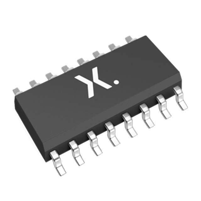
| 描述 | IC SWITCH QUAD 1X1 16SOIC模拟开关 IC QUAD BILATRL ANALOG |
| 产品分类 | |
| 品牌 | NXP Semiconductors |
| 产品手册 | |
| 产品图片 |
|
| rohs | 符合RoHS无铅 / 符合限制有害物质指令(RoHS)规范要求 |
| 产品系列 | 开关 IC,模拟开关 IC,NXP Semiconductors 74HCT4316D,11274HCT |
| 数据手册 | |
| 产品型号 | 74HCT4316D,112 |
| 产品种类 | 模拟开关 IC |
| 供应商器件封装 | 16-SO |
| 其它名称 | 74HCT4316D |
| 功能 | |
| 包装 | 管件 |
| 商标 | NXP Semiconductors |
| 安装类型 | 表面贴装 |
| 安装风格 | SMD/SMT |
| 导通电阻 | 240 欧姆 |
| 导通电阻—最大值 | 320 Ohms |
| 封装 | Tube |
| 封装/外壳 | 16-SOIC(0.154",3.90mm 宽) |
| 封装/箱体 | SO-16 |
| 工作温度 | -40°C ~ 125°C |
| 工作电源电压 | +/- 2.5 V |
| 工厂包装数量 | 1000 |
| 开关配置 | SPST |
| 最大功率耗散 | 500 mW |
| 最大双重电源电压 | +/- 5 V |
| 最大工作温度 | + 125 C |
| 最小工作温度 | - 40 C |
| 标准包装 | 50 |
| 电压-电源,单/双 (±) | 4.5 V ~ 5.5 V, ±1 V ~ 5 V |
| 电压源 | 单/双电源 |
| 电流-电源 | 1nA |
| 电源电压-最大 | 5.5 V |
| 电源电压-最小 | 4.5 V |
| 电路 | 4 x SPST |
| 空闲时间—最大值 | 50 ns |
| 运行时间—最大值 | 56 ns |
| 零件号别名 | 74HCT4316D |


- 商务部:美国ITC正式对集成电路等产品启动337调查
- 曝三星4nm工艺存在良率问题 高通将骁龙8 Gen1或转产台积电
- 太阳诱电将投资9.5亿元在常州建新厂生产MLCC 预计2023年完工
- 英特尔发布欧洲新工厂建设计划 深化IDM 2.0 战略
- 台积电先进制程称霸业界 有大客户加持明年业绩稳了
- 达到5530亿美元!SIA预计今年全球半导体销售额将创下新高
- 英特尔拟将自动驾驶子公司Mobileye上市 估值或超500亿美元
- 三星加码芯片和SET,合并消费电子和移动部门,撤换高东真等 CEO
- 三星电子宣布重大人事变动 还合并消费电子和移动部门
- 海关总署:前11个月进口集成电路产品价值2.52万亿元 增长14.8%


PDF Datasheet 数据手册内容提取
74HC4316; 74HCT4316 Quad single-pole single-throw analog switch Rev. 4 — 15 October 2018 Product data sheet 1. General description The 74HC4316; 74HCT4316 is a quad single pole, single throw analog switch (SPST). Each switch features two input/output terminals (nY and nZ) and an active HIGH enable input (nS). When nS is LOW, the analog switch is turned off. When E is HIGH all four analog switches are turned off. Inputs include clamp diodes. This enables the use of current limiting resistors to interface inputs to voltages in excess of V . CC 2. Features and benefits • Input levels E and nS inputs: • For 74HC4316: CMOS level • For 74HCT4316: TTL level • Low ON resistance: • 160 Ω (typical) at V - V = 4.5 V CC EE • 120 Ω (typical) at V - V = 6.0 V CC EE • 80 Ω (typical) at V - V = 9.0 V CC EE • Logic level translation: • To enable 5 V logic to communicate with ±5 V analog signals • Typical break-before-make built in • Specified in compliance with JEDEC standard no. 7A • ESD protection: • HBM JESD22-A114F exceeds 2000 V • MM JESD22-A115-A exceeds 200 V • Multiple package options • Specified from -40 °C to +85 °C and -40 °C to +125 °C 3. Applications • Signal gating • Modulation • Demodulation • Chopper
Nexperia 74HC4316; 74HCT4316 Quad single-pole single-throw analog switch 4. Ordering information Table 1. Ordering information Type number Package Temperature range Name Description Version 74HC4316D -40 °C to +125 °C SO16 plastic small outline package; 16 leads; body width 3.9 mm SOT109-1 74HCT4316D 74HC4316DB -40 °C to +125 °C SSOP16 plastic shrink small outline package; 16 leads; SOT338-1 body width 5.3 mm 74HCT4316DB 74HC4316PW -40 °C to +125 °C TSSOP16 plastic thin shrink small outline package; 16 leads; SOT403-1 body width 4.4 mm 74HCT4316PW 5. Functional diagram 7 7 G1 G1 2 1 2 1 2 2 2 15 # 15 # 1Y 1 1 X 2 15 1 1S 1Z 3 4 3 4 3 5 2S 2Y 4 5 # 1 5 # 2Z 11 10 11 10 11 6 3Y 3S 6 # 6 # 10 1 3Z 14 12 12 13 12 13 4S 4Y 13 14 # 14 # E 4Z 1 7 (a) (b) aaa-024846 aaa-024847 Fig. 1. Logic symbol Fig. 2. IEC logic symbol 74HC_HCT4316 All information provided in this document is subject to legal disclaimers. © Nexperia B.V. 2018. All rights reserved Product data sheet Rev. 4 — 15 October 2018 2 / 24
Nexperia 74HC4316; 74HCT4316 Quad single-pole single-throw analog switch VCC 16 1 1Z 1S 15 2 1Y 4 2Z 2S 5 3 2Y LOGIC LEVEL 10 3Z CONVERSION 3S 6 AND CONTROL 11 3Y 13 4Z 4S 14 12 4Y E 7 8 9 GND VEE aaa-024848 Fig. 3. Functional diagram nY VCC VEE LOGIC LEVEL E CONVERSION VEE VCC LOGIC LEVEL nS CONVERSION VCC VEE nZ aaa-024850 Fig. 4. Schematic diagram (one switch) 74HC_HCT4316 All information provided in this document is subject to legal disclaimers. © Nexperia B.V. 2018. All rights reserved Product data sheet Rev. 4 — 15 October 2018 3 / 24
Nexperia 74HC4316; 74HCT4316 Quad single-pole single-throw analog switch 6. Pinning information 6.1. Pinning 74HC4316 74HCT4316 74HC4316 1Z 1 16 VCC 74HCT4316 1Y 2 15 1S 1Z 1 16 VCC 2Y 3 14 4S 1Y 2 15 1S 2Y 3 14 4S 2Z 4 13 4Z 2Z 4 13 4Z 2S 5 12 4Y 2S 5 12 4Y 3S 6 11 3Y 3S 6 11 3Y E 7 10 3Z E 7 10 3Z GND 8 9 VEE GND 8 9 VEE aaa-024852 aaa-024851 Fig. 6. Pin configuration SOT338-1 (SSOP16) and Fig. 5. Pin configuration SOT109-1 (SO16) SOT403-1 (TSSOP16) 6.2. Pin description Table 2. Pin description Symbol Pin Description 1Z, 2Z, 3Z, 4Z 1, 4, 10, 13 independent input or output 1Y, 2Y, 3Y, 4Y 2, 3, 11, 12 independent input or output E 7 enable input (active LOW) GND 8 ground (0 V) V 9 negative supply voltage EE 1S, 2S, 3S, 4S 15, 5, 6, 14 select input (active HIGH) V 14 positive supply voltage CC 7. Functional description Table 3. Function table H = HIGH voltage level; L = LOW voltage level; X = don’t care. Input Switch E nS L L OFF L H ON H X OFF 74HC_HCT4316 All information provided in this document is subject to legal disclaimers. © Nexperia B.V. 2018. All rights reserved Product data sheet Rev. 4 — 15 October 2018 4 / 24
Nexperia 74HC4316; 74HCT4316 Quad single-pole single-throw analog switch 8. Limiting values Table 4. Limiting values In accordance with the Absolute Maximum Rating System (IEC 60134). Voltages are referenced to GND (ground = 0 V). Symbol Parameter Conditions Min Max Unit V supply voltage -0.5 +11.0 V CC I input clamping current V < -0.5 V or V > V + 0.5 V - ±20 mA IK I I CC I switch clamping current V < -0.5 V or V > V + 0.5 V - ±20 mA SK SW SW CC I switch current V = -0.5 V to V + 0.5 V [1] - ±25 mA SW SW CC I supply current - 20 mA EE I supply current - 50 mA CC I ground current -50 - mA GND T storage temperature -65 +150 °C stg P total power dissipation T = -40 °C to +125 °C [2] - 500 mW tot amb P power dissipation per switch - 100 mW [1] To avoid drawing VCC current out of terminal nZ, when switch current flows in terminals nY, the voltage drop across the bidirectional switch must not exceed 0.4 V. If the switch current flows into terminal nZ, no VCC current will flow out of terminals nY. In this case there is no limit for the voltage drop across the switch, but the voltages at nY and nZ may not exceed VCC or VEE. [2] For SO16 package: Ptot derates linearly with 8 mW/K above 70 °C. For (T)SSOP16 packages: Ptot derates linearly with 5.5 mW/K above 60 °C. 9. Recommended operating conditions Table 5. Recommended operating conditions Symbol Parameter Conditions 74HC4316 74HCT4316 Unit Min Typ Max Min Typ Max V supply voltage see Fig. 7 and Fig. 8 CC V - GND 2.0 5.0 10.0 4.5 5.0 5.5 V CC V - GND 2.0 5.0 10.0 2.0 5.0 10.0 V EE V input voltage GND - V GND - V V I CC CC V switch voltage V - V V - V V SW EE CC EE CC T ambient temperature -40 +25 +125 -40 +25 +125 °C amb Δt/ΔV input transition rise V = 2.0 V - - 625 - - - ns/V CC and fall rate V = 4.5 V - 1.67 139 - 1.67 139 ns/V CC V = 6.0 V - - 83 - - - ns/V CC V = 10.0 V - - 35 - - - ns/V CC 74HC_HCT4316 All information provided in this document is subject to legal disclaimers. © Nexperia B.V. 2018. All rights reserved Product data sheet Rev. 4 — 15 October 2018 5 / 24
Nexperia 74HC4316; 74HCT4316 Quad single-pole single-throw analog switch 001aad545 001aad546 10 10 VCC - GND VCC - GND (V) (V) 8 8 6 operating area 6 operating area 4 4 2 2 0 0 0 2 4 6 8 10 0 2 4 6 8 10 VCC - VEE (V) VCC - VEE (V) Fig. 7. Guaranteed operating area as a function of the Fig. 8. Guaranteed operating area as a function of the supply voltages for 74HC4316 supply voltages for 74HCT4316 10. Static characteristics Table 6. R resistance per switch for types 74HC4316 and 74HCT4316 ON V = V or V ; for test circuit see Fig. 9. I IH IL V is the input voltage at a nY or nZ terminal, whichever is assigned as an input. is V is the output voltage at a nY or nZ terminal, whichever is assigned as an output. os For 74HC4316: V - GND or V - V = 2.0 V, 4.5 V, 6.0 V and 9.0 V. CC CC EE For 74HCT4316: V - GND = 4.5 V and 5.5 V; V - V = 2.0 V, 4.5 V, 6.0 V and 9.0 V. CC CC EE Symbol Parameter Conditions 25 °C -40 °C to +85 °C -40 °C to +125 °C Unit Typ Max Min Max Min Max R ON resistance V = V to V [1] ON(peak) is CC EE (peak) V = 2.0 V; V = 0 V; - - - - - - Ω CC EE I = 100 μA SW V = 4.5 V; V = 0 V; 160 320 - 400 - 480 Ω CC EE I = 1000 μA SW V = 6.0 V; V = 0 V; 120 240 - 300 - 360 Ω CC EE I = 1000 μA SW V = 4.5 V; V = -4.5 V; 85 170 - 215 - 255 Ω CC EE I = 1000 μA SW 74HC_HCT4316 All information provided in this document is subject to legal disclaimers. © Nexperia B.V. 2018. All rights reserved Product data sheet Rev. 4 — 15 October 2018 6 / 24
Nexperia 74HC4316; 74HCT4316 Quad single-pole single-throw analog switch Symbol Parameter Conditions 25 °C -40 °C to +85 °C -40 °C to +125 °C Unit Typ Max Min Max Min Max R ON resistance V = V [1] ON(rail) is EE (rail) V = 2.0 V; V = 0 V; 160 - - - - - Ω CC EE I = 100 μA SW V = 4.5 V; V = 0 V; 80 160 - 200 - 240 Ω CC EE I = 1000 μA SW V = 6.0 V; V = 0 V; 70 140 - 175 - 210 Ω CC EE I = 1000 μA SW V = 4.5 V; V = -4.5 V; 60 120 - 150 - 180 Ω CC EE I = 1000 μA SW V = V [1] is CC V = 2.0 V; V = 0 V; 170 - - - - - Ω CC EE I = 100 μA SW V = 4.5 V; V = 0 V; 90 180 - 225 - 270 Ω CC EE I = 1000 μA SW V = 6.0 V; V = 0 V; 80 160 - 200 - 240 Ω CC EE I = 1000 μA SW V = 4.5 V; V = -4.5 V; 65 135 - 170 - 205 Ω CC EE I = 1000 μA SW ΔR ON resistance V = V to V [1] ON is CC EE mismatch V = 2.0 V; V = 0 V - - - - - - Ω CC EE between channels VCC = 4.5 V; VEE = 0 V 16 - - - - - Ω V = 6.0 V; V = 0 V 9 - - - - - Ω CC EE V = 4.5 V; V = -4.5 V 6 - - - - - Ω CC EE [1] When supply voltages (VCC - VEE) near 2.0 V the analog switch ON resistance becomes extremely non-linear. When using a supply of 2 V, it is recommended to use these devices only for transmitting digital signals. aaa-024854 200 RON Vsw (Ω) VCC = 4.5 V V VCC VIH nS 100 VCC = 6.0 V VIL E VCC = 9.0 V nY nZ Vis GND VEE Isw aaa-024853 0 Vis = 0 V to (VCC - VEE) 0 5 10 Vis (V) V = 0 V to (V - V ) is CC EE Fig. 9. Test circuit for measuring R Fig. 10. Typical R as a function of input voltage V ON ON is 74HC_HCT4316 All information provided in this document is subject to legal disclaimers. © Nexperia B.V. 2018. All rights reserved Product data sheet Rev. 4 — 15 October 2018 7 / 24
Nexperia 74HC4316; 74HCT4316 Quad single-pole single-throw analog switch Table 7. Static characteristics 74HC4316 At recommended operating conditions; voltages are referenced to GND (ground = 0 V). V is the input voltage at a nY or nZ terminal, whichever is assigned as an input. is V is the output voltage at a nY or nZ terminal, whichever is assigned as an output. os Symbol Parameter Conditions Min Typ Max Unit T = 25 °C amb V HIGH-level input voltage V = 2.0 V 1.5 1.2 - V IH CC V = 4.5 V 3.15 2.4 - V CC V = 6.0 V 4.2 3.2 - V CC V = 9.0 V 6.3 4.3 - V CC V LOW-level input voltage V = 2.0 V - 0.8 0.5 V IL CC V = 4.5 V - 2.1 1.35 V CC V = 6.0 V - 2.8 1.8 V CC V = 9.0 V - 4.3 2.7 V CC I input leakage current V = V or GND I I CC V = 6.0 V; V = 0 V - - ±0.1 μA CC EE V = 10.0 V; V = 0 V - - ±0.2 μA CC EE I OFF-state leakage current V = 10.0 V; V = 0 V; V = V or V ; - - ±0.1 μA S(OFF) CC EE I IH IL |V | = V - V ; see Fig. 11 SW CC EE I ON-state leakage current V = 10.0 V; V = 0 V; V = V or V ; - - ±0.1 μA S(ON) CC EE I IH IL |V | = V - V ; see Fig. 12 SW CC EE I supply current V = V or GND; V = V or V ; CC I CC is EE CC V = V or V os CC EE V = 6.0 V; V = 0 V - - 8.0 μA CC EE V = 10.0 V; V = 0 V - - 16.0 μA CC EE C input capacitance - 3.5 - pF I C switch capacitance - 5 - pF sw T = -40 °C to +85 °C amb V HIGH-level input voltage V = 2.0 V 1.5 - - V IH CC V = 4.5 V 3.15 - - V CC V = 6.0 V 4.2 - - V CC V = 9.0 V 6.3 - - V CC V LOW-level input voltage V = 2.0 V - - 0.5 V IL CC V = 4.5 V - - 1.35 V CC V = 6.0 V - - 1.8 V CC V = 9.0 V - - 2.7 V CC I input leakage current V = V or GND I I CC V = 6.0 V; V = 0 V - - ±1.0 μA CC EE V = 10.0 V; V = 0 V - - ±2.0 μA CC EE I OFF-state leakage current V = 10.0 V; V = 0 V; V = V or V ; - - ±1.0 μA S(OFF) CC EE I IH IL |V | = V - V ; see Fig. 11 SW CC EE I ON-state leakage current V = 10.0 V; V = 0 V; V = V or V ; - - ±1.0 μA S(ON) CC EE I IH IL |V | = V - V ; see Fig. 12 SW CC EE I supply current V = V or GND; V = V or V ; CC I CC is EE CC V = V or V os CC EE V = 6.0 V; V = 0 V - - 80.0 μA CC EE V = 10.0 V; V = 0 V - - 160.0 μA CC EE 74HC_HCT4316 All information provided in this document is subject to legal disclaimers. © Nexperia B.V. 2018. All rights reserved Product data sheet Rev. 4 — 15 October 2018 8 / 24
Nexperia 74HC4316; 74HCT4316 Quad single-pole single-throw analog switch Symbol Parameter Conditions Min Typ Max Unit T = -40 °C to +125 °C amb V HIGH-level input voltage V = 2.0 V 1.5 - - V IH CC V = 4.5 V 3.15 - - V CC V = 6.0 V 4.2 - - V CC V = 9.0 V 6.3 - - V CC V LOW-level input voltage V = 2.0 V - - 0.5 V IL CC V = 4.5 V - - 1.35 V CC V = 6.0 V - - 1.8 V CC V = 9.0 V - - 2.7 V CC I input leakage current V = V or GND I I CC V = 6.0 V; V = 0 V - - ±1.0 μA CC EE V = 10.0 V; V = 0 V - - ±2.0 μA CC EE I OFF-state leakage current V = 10.0 V; V = 0 V; V = V or V ; - - ±1.0 μA S(OFF) CC EE I IH IL |V | = V - V ; see Fig. 11 SW CC EE I ON-state leakage current V = 10.0 V; V = 0 V; V = V or V ; - - ±1.0 μA S(ON) CC EE I IH IL |V | = V - V ; see Fig. 12 SW CC EE I supply current V = V or GND; V = V or V ; CC I CC is EE CC V = V or V os CC EE V = 6.0 V; V = 0 V - - 160 μA CC EE V = 10.0 V; V = 0 V - - 320 μA CC EE Table 8. Static characteristics 74HCT4316 At recommended operating conditions; voltages are referenced to GND (ground = 0 V). V is the input voltage at a nY or nZ terminal, whichever is assigned as an input. is V is the output voltage at a nY or nZ terminal, whichever is assigned as an output. os Symbol Parameter Conditions Min Typ Max Unit T = 25 °C amb V HIGH-level input voltage V = 4.5 V to 5.5 V 2.0 1.6 - V IH CC V LOW-level input voltage V = 4.5 V to 5.5 V - 1.2 0.8 V IL CC I input leakage current V = V or GND; V = 5.5 V; V = 0 V - - ±0.1 μA I I CC CC EE I OFF-state leakage current V = 10 V; V = 0 V; V = V or V ; - - ±0.1 μA S(OFF) CC EE I IH IL |V | = V - V ; see Fig. 11 SW CC EE I ON-state leakage current V = 10 V; V = 0 V; V = V or V ; - - ±0.1 μA S(ON) CC EE I IH IL |V | = V - V ; see Fig. 12 SW CC EE I supply current V = V or GND; V = V or V ; CC I CC is EE CC V = V or V os CC EE V = 5.5 V; V = 0 V - - 8.0 μA CC EE V = 5.0 V; V = -5.0 V - - 16.0 μA CC EE ΔI additional supply current nS and E; per input pin; V = V - 2.1 V; - 50 180 μA CC I CC other inputs at V or GND; CC V = 4.5 V to 5.5 V; V = 0 V CC EE C input capacitance - 3.5 - pF I C switch capacitance - 5 - pF sw 74HC_HCT4316 All information provided in this document is subject to legal disclaimers. © Nexperia B.V. 2018. All rights reserved Product data sheet Rev. 4 — 15 October 2018 9 / 24
Nexperia 74HC4316; 74HCT4316 Quad single-pole single-throw analog switch Symbol Parameter Conditions Min Typ Max Unit T = -40 °C to +85 °C amb V HIGH-level input voltage V = 4.5 V to 5.5 V 2.0 - - V IH CC V LOW-level input voltage V = 4.5 V to 5.5 V - - 0.8 V IL CC I input leakage current V = V or GND; V = 5.5 V; V = 0 V - - ±1.0 μA I I CC CC EE I OFF-state leakage current V = 10 V; V = 0 V; V = V or V ; - - ±1.0 μA S(OFF) CC EE I IH IL |V | = V - V ; see Fig. 11 SW CC EE I ON-state leakage current V = 10 V; V = 0 V; V = V or V ; - - ±1.0 μA S(ON) CC EE I IH IL |V | = V - V ; see Fig. 12 SW CC EE I supply current V = V or GND; V = V or V ; CC I CC is EE CC V = V or V os CC EE V = 5.5 V; V = 0 V - - 80 μA CC EE V = 5.0 V; V = -5.0 V - - 160 μA CC EE ΔI additional supply current nS and E; per input pin; V = V - 2.1 V; - - 225 μA CC I CC other inputs at V or GND; CC V = 4.5 V to 5.5 V; V = 0 V CC EE T = -40 °C to +125 °C amb V HIGH-level input voltage V = 4.5 V to 5.5 V 2.0 - - V IH CC V LOW-level input voltage V = 4.5 V to 5.5 V - - 0.8 V IL CC I input leakage current V = V or GND; V = 5.5 V; V = 0 V - - ±1.0 μA I I CC CC EE I OFF-state leakage current V = 10 V; V = 0 V; V = V or V ; - - ±1.0 μA S(OFF) CC EE I IH IL |V | = V - V ; see Fig. 11 SW CC EE I ON-state leakage current V = 10 V; V = 0 V; V = V or V ; - - ±1.0 μA S(ON) CC EE I IH IL |V | = V - V ; see Fig. 12 SW CC EE I supply current V = V or GND; V = V or V ; CC I CC is EE CC V = V or V os CC EE V = 5.5 V; V = 0 V - - 160 μA CC EE V = 5.0 V; V = -5.0 V - - 320 μA CC EE ΔI additional supply current nS and E; per input pin; V = V - 2.1 V; - - 245 μA CC I CC other inputs at V or GND; CC V = 4.5 V to 5.5 V; V = 0 V CC EE VCC VCC nS nS VIL VIH E E VIH Isw Isw VIL Isw nY nZ nY nZ A A A Vos Vis GND VEE Vos Vis GND VEE aaa-024855 aaa-024856 V = V and V = V V = V and V = open is CC os EE is CC os V = V and V = V V = V and V = open is EE os CC is EE os Fig. 11. Test circuit for measuring OFF-state leakage Fig. 12. Test circuit for measuring ON-state leakage current current 74HC_HCT4316 All information provided in this document is subject to legal disclaimers. © Nexperia B.V. 2018. All rights reserved Product data sheet Rev. 4 — 15 October 2018 10 / 24
Nexperia 74HC4316; 74HCT4316 Quad single-pole single-throw analog switch 11. Dynamic characteristics Table 9. Dynamic characteristics GND = 0 V; t = t = 6 ns; C = 50 pF unless specified otherwise; for test circuit see Fig. 15. r f L V is the input voltage at a nY or nZ terminal, whichever is assigned as an input. is V is the output voltage at a nY or nZ terminal, whichever is assigned as an output. os Symbol Parameter Conditions 25 °C -40 °C to +85 °C -40 °C to +125 °C Unit Typ Max Min Max Min Max 74HC4316 t propagation nY to nZ or nZ to nY; R = ∞ Ω; [1] pd L delay see Fig. 13 V = 2.0 V; V = 0 V 17 60 - 75 - 90 ns CC EE V = 4.5 V; V = 0 V 6 12 - 15 - 18 ns CC EE V = 6.0 V; V = 0 V 5 10 - 13 - 15 ns CC EE V = 4.5 V; V = -4.5 V 4 8 - 10 - 12 ns CC EE t turn-off time E to nY or nZ; see Fig. 14 [2] off V = 2.0 V; V = 0 V 63 220 - 275 - 330 ns CC EE V = 4.5 V; V = 0 V 23 44 - 55 - 66 ns CC EE V = 5.0 V; V = 0 V;C = 15 pF 20 - - - - - ns CC EE L V = 6.0 V; V = 0 V 18 37 - 47 - 56 ns CC EE V = 4.5 V; V = -4.5 V 21 39 - 49 - 59 ns CC EE nS to nY or nZ; see Fig. 14 [2] V = 2.0 V; V = 0 V 55 175 - 220 - 265 ns CC EE V = 4.5 V; V = 0 V 20 35 - 44 - 53 ns CC EE V = 5.0 V; V = 0 V; C = 15 pF 16 - - - - - ns CC EE L V = 6.0 V; V = 0 V 16 30 - 37 - 45 ns CC EE V = 4.5 V; V = -4.5 V 18 36 - 45 - 54 ns CC EE t turn-on time E to nY or nZ; see Fig. 14 [3] on V = 2.0 V; V = 0 V 61 205 - 255 - 310 ns CC EE V = 4.5 V; V = 0 V 22 41 - 51 - 62 ns CC EE V = 5.0 V; V = 0 V; C = 15 pF 19 - - - - - ns CC EE L V = 6.0 V; V = 0 V 18 35 - 43 - 53 ns CC EE V = 4.5 V; V = -4.5 V 19 37 - 47 - 56 ns CC EE nS to nY or nZ; see Fig. 14 [3] V = 2.0 V; V = 0 V 52 175 - 220 - 265 ns CC EE V = 4.5 V; V = 0 V 19 35 - 44 - 53 ns CC EE V = 5.0 V; V = 0 V; C = 15 pF 16 - - - - - ns CC EE L V = 6.0 V; V = 0 V 15 30 - 37 - 45 ns CC EE V = 4.5 V; V = -4.5 V 17 34 - 43 - 51 ns CC EE C power per switch; V = GND to V [4] 13 - - - - - pF PD I CC dissipation capacitance 74HC_HCT4316 All information provided in this document is subject to legal disclaimers. © Nexperia B.V. 2018. All rights reserved Product data sheet Rev. 4 — 15 October 2018 11 / 24
Nexperia 74HC4316; 74HCT4316 Quad single-pole single-throw analog switch Symbol Parameter Conditions 25 °C -40 °C to +85 °C -40 °C to +125 °C Unit Typ Max Min Max Min Max 74HCT4316 t propagation nY to nZ or nZ to nY; R = ∞ Ω; [1] pd L delay see Fig. 13 V = 4.5 V; V = 0 V 6 12 - 15 - 18 ns CC EE V = 4.5 V; V = -4.5 V 4 8 - 10 - 12 ns CC EE t OFF-state E to nY or nZ; see Fig. 14 PZH to HIGH V = 4.5 V; V = 0 V 22 44 - 55 - 66 ns CC EE propagation delay VCC = 5.0 V; VEE = 0 V; CL = 15 pF 19 - - - - - ns V = 4.5 V; V = -4.5 V 21 42 - 53 - 63 ns CC EE nS to nY or nZ; see Fig. 14 V = 4.5 V; V = 0 V 20 40 - 53 - 60 ns CC EE V = 5.0 V; V = 0 V; C = 15 pF 17 - - - - - ns CC EE L V = 4.5 V; V = -4.5 V 17 34 - 43 - 51 ns CC EE t OFF-state E to nY or nZ; see Fig. 14 PZL to LOW V = 4.5 V; V = 0 V 28 56 - 70 - 84 ns CC EE propagation delay VCC = 5.0 V; VEE = 0 V; CL = 15 pF 24 - - - - - ns V = 4.5 V; V = -4.5 V 21 42 - 53 - 63 ns CC EE nS to nY or nZ; see Fig. 14 V = 4.5 V; V = 0 V 25 50 - 63 - 75 ns CC EE V = 5.0 V; V = 0 V; C = 15 pF 21 - - - - - ns CC EE L V = 4.5 V; V = -4.5 V 17 34 - 43 - 51 ns CC EE t turn-off time E to nY or nZ; see Fig. 14 [2] off V = 4.5 V; V = 0 V 25 50 - 63 - 75 ns CC EE V = 5.0 V; V = 0 V; C = 15 pF 21 - - - - - ns CC EE L V = 4.5 V; V = -4.5 V 23 46 - 58 - 69 ns CC EE nS to nY or nZ; see Fig. 14 [2] V = 4.5 V; V = 0 V 22 44 - 55 - 66 ns CC EE V = 5.0 V; V = 0 V; C = 15 pF 19 - - - - - ns CC EE L V = 4.5 V; V = -4.5 V 20 40 - 50 - 60 ns CC EE C power per switch; V = GND to (V - 1.5 V) [4] 14 - - - - - pF PD I CC dissipation capacitance [1] tpd is the same as tPHL and tPLH. [2] toff is the same as tPHZ and tPLZ. [3] ton is the same as tPZH and tPZL. [4] CPD is used to determine the dynamic power dissipation (PD in μW). PD = CPD x VCC2 x fi + ∑((CL + Csw) x VCC2 x fo) where: fi = input frequency in MHz; fo = output frequency in MHz; ∑((CL + Csw) x VCC2 x fo) = sum of outputs; CL = output load capacitance in pF; Csw = switch capacitance in pF; VCC = supply voltage in V. 74HC_HCT4316 All information provided in this document is subject to legal disclaimers. © Nexperia B.V. 2018. All rights reserved Product data sheet Rev. 4 — 15 October 2018 12 / 24
Nexperia 74HC4316; 74HCT4316 Quad single-pole single-throw analog switch 11.1. Waveforms and test circuit Vis input 50 % tPLH tPHL Vos output 50 % 001aad555 Fig. 13. Input (V ) to output (V ) propagation delays is os VI nS, E input VM 0 V tPLZ tPZL Vos output 50 % 10 % tPHZ tPZH 90 % 50 % Vos output switch ON switch OFF switch ON aaa-024857 Measurement points are shown in Table 10. Fig. 14. Turn-on and turn-off times Table 10. Measurement points Type V V I M 74HC4316 V 0.5V CC CC 74HCT4316 3.0 V 1.3 V 74HC_HCT4316 All information provided in this document is subject to legal disclaimers. © Nexperia B.V. 2018. All rights reserved Product data sheet Rev. 4 — 15 October 2018 13 / 24
Nexperia 74HC4316; 74HCT4316 Quad single-pole single-throw analog switch tW VI 90 % negative pulse VM VM 10 % 0 V tf tr tr tf VI 90 % positive pulse VM VM 10 % 0 V tW VCC Vis VCC PULSE VI Vos RL S1 DUT open GENERATOR RT CL GND VEE aaa-024858 Test data is given in Table 11. Definitions test circuit: R = Termination resistance should be equal to output impedance Z of the pulse generator. T o C = Load capacitance including jig and probe capacitance. L R = Load resistance. L S1 = Test selection switch. Fig. 15. Test circuit for measuring switching times Table 11. Test data Test Input Output S1 position E nS Switch nY (nZ) t, t Switch nZ (nY) r f V V at f other [1] C R I is max L L t t [2] GND to V < 2 ns 6 ns 50 pF - open PHL, PLH CC t , t [2] V < 2 ns 6 ns 50 pF, 15 pF 1 kΩ V PHZ PZH CC EE t , t [2] V < 2 ns 6 ns 50 pF, 15 pF 1 kΩ V PLZ PZL EE CC [1] tr = tf = 6 ns; when measuring fmax, there is no constraint to tr and tf with 50 % duty factor. [2] VI values: For 74HC4316: VI = VCC For 74HCT4316: VI = 3 V 74HC_HCT4316 All information provided in this document is subject to legal disclaimers. © Nexperia B.V. 2018. All rights reserved Product data sheet Rev. 4 — 15 October 2018 14 / 24
Nexperia 74HC4316; 74HCT4316 Quad single-pole single-throw analog switch 11.2. Additional dynamic characteristics Table 12. Additional dynamic characteristics Recommended conditions and typical values; GND = 0 V; T = 25 °C; C = 50 pF. amb L V is the input voltage at a nY or nZ terminal, whichever is assigned as an input. is V is the output voltage at a nY or nZ terminal, whichever is assigned as an output. os Symbol Parameter Conditions Min Typ Max Unit THD total harmonic f = 1 kHz; R = 10 kΩ; see Fig. 16 i L distortion V = 4.0 V (p-p); V = 2.25 V; V = -2.25 V - 0.80 - % is CC EE V = 8.0 V (p-p); V = 4.5 V; V = -4.5 V - 0.40 - % is CC EE f = 10 kHz; R = 10 kΩ; see Fig. 16 i L V = 4.0 V (p-p); V = 2.25 V; V = -2.25 V - 2.40 - % is CC EE V = 8.0 V (p-p); V = 4.5 V; V = -4.5 V - 1.20 - % is CC EE f -3 dB frequency R = 50 Ω; C = 10 pF; see Fig. 17 [1] (-3dB) L L response V = 2.25 V; V = -2.25 V - 150 - MHz CC EE V = 4.5 V; V = -4.5 V - 160 - MHz CC EE α isolation (OFF-state) R = 600 Ω; f = 1 MHz; see Fig. 18 [2] iso L i V = 2.25 V; V = -2.25 V - -50 - dB CC EE V = 4.5 V; V = -4.5 V - -50 - dB CC EE V crosstalk voltage between digital input and switch (peak to peak value); ct R = 600 Ω; f = 1 MHz; E or nS square wave between L i V and GND; t = t = 6 ns; see Fig. 19 CC r f V = 4.5 V; V = 0 V - 110 - mV CC EE V = 4.5 V; V = -4.5 V - 220 - mV CC EE Xtalk crosstalk between switches; R = 600 Ω; f = 1 MHz; see Fig. 20 [2] L i V = 2.25 V; V = -2.25 V - -60 - dB CC EE V = 4.5 V; V = -4.5 V - -60 - dB CC EE [1] Adjust input voltage Vis to 0 dBm level at Vos for 1 MHz (0 dBm = 1 mW into 50 Ω). [2] Adjust input voltage Vis to 0 dBm level (0 dBm = 1 mW into 600 Ω). VCC nS VIH E VIL 10 µF nYn/nZ nZ/nYn Vis Vos VEE GND RL CL dB aaa-024860 Fig. 16. Test circuit for measuring total harmonic distortion 74HC_HCT4316 All information provided in this document is subject to legal disclaimers. © Nexperia B.V. 2018. All rights reserved Product data sheet Rev. 4 — 15 October 2018 15 / 24
Nexperia 74HC4316; 74HCT4316 Quad single-pole single-throw analog switch VCC nS VIH E VIL 0.1 µF nYn/nZ nZ/nYn Vis Vos VEE GND RL CL dB aaa-024861 V = 4.5 V; GND = 0 V; V = -4.5 V; R = 50 Ω; R = 1 kΩ. CC EE L S a. Test circuit aaa-024862 5 (dB) 0 -5 10 102 103 104 105 106 fi (kHz) b. Typical -3 dB frequency response Fig. 17. -3 dB frequency response 74HC_HCT4316 All information provided in this document is subject to legal disclaimers. © Nexperia B.V. 2018. All rights reserved Product data sheet Rev. 4 — 15 October 2018 16 / 24
Nexperia 74HC4316; 74HCT4316 Quad single-pole single-throw analog switch VCC nS VIH E VIL 0.1 µF nYn/nZ nZ/nYn Vis Vos VEE GND RL CL dB aaa-024861 V = 4.5 V; GND = 0 V; V = -4.5 V; R = 600 Ω; R = 1 kΩ. CC EE L S a. Test circuit 001aae332 0 αiso (dB) -20 -40 -60 -80 -100 10 102 103 104 105 106 fi (kHz) b. Isolation (OFF-state) as a function of frequency Fig. 18. Isolation (OFF-state) as a function of frequency 2RL VCC 2RL Vct nS, E nY nZ G 2RL VEE GND 2RL oscilloscope aaa-024863 Fig. 19. Test circuit for measuring crosstalk voltage (between the digital input and the switch) 74HC_HCT4316 All information provided in this document is subject to legal disclaimers. © Nexperia B.V. 2018. All rights reserved Product data sheet Rev. 4 — 15 October 2018 17 / 24
Nexperia 74HC4316; 74HCT4316 Quad single-pole single-throw analog switch VCC nS VIH E VIL 0.1 µF RL nY/nZ nZ/nY Vis VEE GND RL CL VCC nS VIL E VIH nY/nZ nZ/nY Vos RL VEE GND RL CL dB aaa-024864 Fig. 20. Test circuit for measuring crosstalk (between the switches) 74HC_HCT4316 All information provided in this document is subject to legal disclaimers. © Nexperia B.V. 2018. All rights reserved Product data sheet Rev. 4 — 15 October 2018 18 / 24
Nexperia 74HC4316; 74HCT4316 Quad single-pole single-throw analog switch 12. Package outline SO16: plastic small outline package; 16 leads; body width 3.9 mm SOT109-1 D E A X c y H E v M A Z 16 9 Q A 2 A 1 (A 3 ) A pin 1 index θ L p 1 8 L e w M detail X b p 0 2.5 5 mm scale DIMENSIONS (inch dimensions are derived from the original mm dimensions) UNIT mAax . A 1 A 2 A 3 b p c D (1) E (1) e H E L L p Q v w y Z (1) θ 0.25 1.45 0.49 0.25 10.0 4.0 6.2 1.0 0.7 0.7 mm 1.75 0.25 1.27 1.05 0.2 5 0.25 0.1 0.10 1.25 0.36 0.19 9.8 3.8 5.8 0.4 0.6 0.3 8 o 0.010 0.057 0.019 0.0100 0.39 0.16 0.244 0.039 0.028 0.028 0 o inches 0.069 0.01 0.05 0.041 0.01 0.01 0.004 0.004 0.049 0.014 0.0075 0.38 0.15 0.228 0.016 0.020 0.012 Note 1. Plastic or metal protrusions of 0.15 mm (0.006 inch) maximum per side are not included. OUTLINE REFERENCES EUROPEAN ISSUE DATE VERSION IEC JEDEC JEITA PROJECTION 99-12-27 SOT109-1 076E07 MS-012 03-02-19 Fig. 21. Package outline SOT109-1 (SO16) 74HC_HCT4316 All information provided in this document is subject to legal disclaimers. © Nexperia B.V. 2018. All rights reserved Product data sheet Rev. 4 — 15 October 2018 19 / 24
Nexperia 74HC4316; 74HCT4316 Quad single-pole single-throw analog switch SSOP16: plastic shrink small outline package; 16 leads; body width 5.3 mm SOT338-1 D E A X c y H E v M A Z 16 9 Q A 2 A 1 (A 3 ) A pin 1 index θ L p L 1 8 detail X w M e b p 0 2.5 5 mm scale DIMENSIONS (mm are the original dimensions) UNIT mAax . A 1 A 2 A 3 b p c D (1) E (1) e H E L L p Q v w y Z (1) θ 0.21 1.80 0.38 0.20 6.4 5.4 7.9 1.03 0.9 1.00 8 o mm 2 0.05 1.65 0.25 0.25 0.09 6.0 5.2 0.65 7.6 1.25 0.63 0.7 0.2 0.13 0.1 0.55 0 o Note 1. Plastic or metal protrusions of 0.25 mm maximum per side are not included. OUTLINE REFERENCES EUROPEAN ISSUE DATE VERSION IEC JEDEC JEITA PROJECTION 99-12-27 SOT338-1 MO-150 03-02-19 Fig. 22. Package outline SOT338-1 (SSOP16) 74HC_HCT4316 All information provided in this document is subject to legal disclaimers. © Nexperia B.V. 2018. All rights reserved Product data sheet Rev. 4 — 15 October 2018 20 / 24
Nexperia 74HC4316; 74HCT4316 Quad single-pole single-throw analog switch TSSOP16: plastic thin shrink small outline package; 16 leads; body width 4.4 mm SOT403-1 D E A X c y H E v M A Z 16 9 Q A 2 (A 3 ) A pin 1 index A 1 θ L p L 1 8 detail X w M e b p 0 2.5 5 mm scale DIMENSIONS (mm are the original dimensions) UNIT mAax . A 1 A 2 A 3 b p c D (1) E (2) e H E L L p Q v w y Z (1) θ 0.15 0.95 0.30 0.2 5.1 4.5 6.6 0.75 0.4 0.40 8 o mm 1.1 0.05 0.80 0.25 0.19 0.1 4.9 4.3 0.65 6.2 1 0.50 0.3 0.2 0.13 0.1 0.06 0 o Notes 1. Plastic or metal protrusions of 0.15 mm maximum per side are not included. 2. Plastic interlead protrusions of 0.25 mm maximum per side are not included. OUTLINE REFERENCES EUROPEAN ISSUE DATE VERSION IEC JEDEC JEITA PROJECTION 99-12-27 SOT403-1 MO-153 03-02-18 Fig. 23. Package outline SOT403-1 (TSSOP16) 74HC_HCT4316 All information provided in this document is subject to legal disclaimers. © Nexperia B.V. 2018. All rights reserved Product data sheet Rev. 4 — 15 October 2018 21 / 24
Nexperia 74HC4316; 74HCT4316 Quad single-pole single-throw analog switch 13. Abbreviations Table 13. Abbreviations Acronym Description CMOS Complementary Metal-Oxide Semiconductor DUT Device Under Test ESD ElectroStatic Discharge HBM Human Body Model MM Machine Model TTL Transistor-Transistor Logic 14. Revision history Table 14. Revision history Document ID Release date Data sheet status Change notice Supersedes 74HC_HCT4316 v.4 20181016 Product data sheet - 74HC_HCT4316 v.3 Modifications: • The format of this data sheet has been redesigned to comply with the identity guidelines of Nexperia. • Legal texts have been adapted to the new company name where appropriate. 74HC_HCT4316 v.3 20170102 Product data sheet - 74HC_HCT4316_CNV v.2 Modifications: • The format of this data sheet has been redesigned to comply with the new identity guidelines of NXP Semiconductors. • Legal texts have been adapted to the new company name where appropriate. • Type numbers 74HC4316N and 74HCT4316N removed. 74HC_HCT4316_CNV v.2 19930901 Product specification - - 74HC_HCT4316 All information provided in this document is subject to legal disclaimers. © Nexperia B.V. 2018. All rights reserved Product data sheet Rev. 4 — 15 October 2018 22 / 24
Nexperia 74HC4316; 74HCT4316 Quad single-pole single-throw analog switch injury, death or severe property or environmental damage. Nexperia and its 15. Legal information suppliers accept no liability for inclusion and/or use of Nexperia products in such equipment or applications and therefore such inclusion and/or use is at the customer’s own risk. Quick reference data — The Quick reference data is an extract of the Data sheet status product data given in the Limiting values and Characteristics sections of this document, and as such is not complete, exhaustive or legally binding. Document status Product Definition Applications — Applications that are described herein for any of these [1][2] status [3] products are for illustrative purposes only. Nexperia makes no representation Objective [short] Development This document contains data from or warranty that such applications will be suitable for the specified use data sheet the objective specification for without further testing or modification. product development. Customers are responsible for the design and operation of their applications and products using Nexperia products, and Nexperia accepts no liability for Preliminary [short] Qualification This document contains data from any assistance with applications or customer product design. It is customer’s data sheet the preliminary specification. sole responsibility to determine whether the Nexperia product is suitable Product [short] Production This document contains the product and fit for the customer’s applications and products planned, as well as data sheet specification. for the planned application and use of customer’s third party customer(s). Customers should provide appropriate design and operating safeguards to minimize the risks associated with their applications and products. [1] Please consult the most recently issued document before initiating or completing a design. Nexperia does not accept any liability related to any default, damage, costs [2] The term 'short data sheet' is explained in section "Definitions". or problem which is based on any weakness or default in the customer’s [3] The product status of device(s) described in this document may have applications or products, or the application or use by customer’s third party changed since this document was published and may differ in case of customer(s). Customer is responsible for doing all necessary testing for the multiple devices. The latest product status information is available on customer’s applications and products using Nexperia products in order to the internet at https://www.nexperia.com. avoid a default of the applications and the products or of the application or use by customer’s third party customer(s). Nexperia does not accept any liability in this respect. Definitions Limiting values — Stress above one or more limiting values (as defined in Draft — The document is a draft version only. The content is still under the Absolute Maximum Ratings System of IEC 60134) will cause permanent internal review and subject to formal approval, which may result in damage to the device. Limiting values are stress ratings only and (proper) modifications or additions. Nexperia does not give any representations or operation of the device at these or any other conditions above those warranties as to the accuracy or completeness of information included herein given in the Recommended operating conditions section (if present) or the and shall have no liability for the consequences of use of such information. Characteristics sections of this document is not warranted. Constant or repeated exposure to limiting values will permanently and irreversibly affect Short data sheet — A short data sheet is an extract from a full data sheet the quality and reliability of the device. with the same product type number(s) and title. A short data sheet is intended for quick reference only and should not be relied upon to contain Terms and conditions of commercial sale — Nexperia products are detailed and full information. For detailed and full information see the relevant sold subject to the general terms and conditions of commercial sale, as full data sheet, which is available on request via the local Nexperia sales published at http://www.nexperia.com/profile/terms, unless otherwise agreed office. In case of any inconsistency or conflict with the short data sheet, the in a valid written individual agreement. In case an individual agreement is full data sheet shall prevail. concluded only the terms and conditions of the respective agreement shall apply. Nexperia hereby expressly objects to applying the customer’s general Product specification — The information and data provided in a Product terms and conditions with regard to the purchase of Nexperia products by data sheet shall define the specification of the product as agreed between customer. Nexperia and its customer, unless Nexperia and customer have explicitly agreed otherwise in writing. In no event however, shall an agreement be No offer to sell or license — Nothing in this document may be interpreted valid in which the Nexperia product is deemed to offer functions and qualities or construed as an offer to sell products that is open for acceptance or the beyond those described in the Product data sheet. grant, conveyance or implication of any license under any copyrights, patents or other industrial or intellectual property rights. Export control — This document as well as the item(s) described herein Disclaimers may be subject to export control regulations. Export might require a prior Limited warranty and liability — Information in this document is believed authorization from competent authorities. to be accurate and reliable. However, Nexperia does not give any Non-automotive qualified products — Unless this data sheet expressly representations or warranties, expressed or implied, as to the accuracy states that this specific Nexperia product is automotive qualified, the or completeness of such information and shall have no liability for the product is not suitable for automotive use. It is neither qualified nor tested in consequences of use of such information. Nexperia takes no responsibility accordance with automotive testing or application requirements. Nexperia for the content in this document if provided by an information source outside accepts no liability for inclusion and/or use of non-automotive qualified of Nexperia. products in automotive equipment or applications. In no event shall Nexperia be liable for any indirect, incidental, punitive, In the event that customer uses the product for design-in and use in special or consequential damages (including - without limitation - lost automotive applications to automotive specifications and standards, profits, lost savings, business interruption, costs related to the removal customer (a) shall use the product without Nexperia’s warranty of the or replacement of any products or rework charges) whether or not such product for such automotive applications, use and specifications, and (b) damages are based on tort (including negligence), warranty, breach of whenever customer uses the product for automotive applications beyond contract or any other legal theory. Nexperia’s specifications such use shall be solely at customer’s own risk, Notwithstanding any damages that customer might incur for any reason and (c) customer fully indemnifies Nexperia for any liability, damages or failed whatsoever, Nexperia’s aggregate and cumulative liability towards customer product claims resulting from customer design and use of the product for for the products described herein shall be limited in accordance with the automotive applications beyond Nexperia’s standard warranty and Nexperia’s Terms and conditions of commercial sale of Nexperia. product specifications. Right to make changes — Nexperia reserves the right to make changes Translations — A non-English (translated) version of a document is for to information published in this document, including without limitation reference only. The English version shall prevail in case of any discrepancy specifications and product descriptions, at any time and without notice. This between the translated and English versions. document supersedes and replaces all information supplied prior to the publication hereof. Trademarks Suitability for use — Nexperia products are not designed, authorized or warranted to be suitable for use in life support, life-critical or safety-critical Notice: All referenced brands, product names, service names and systems or equipment, nor in applications where failure or malfunction trademarks are the property of their respective owners. of an Nexperia product can reasonably be expected to result in personal 74HC_HCT4316 All information provided in this document is subject to legal disclaimers. © Nexperia B.V. 2018. All rights reserved Product data sheet Rev. 4 — 15 October 2018 23 / 24
Nexperia 74HC4316; 74HCT4316 Quad single-pole single-throw analog switch Contents 1. General description......................................................1 2. Features and benefits..................................................1 3. Applications..................................................................1 4. Ordering information....................................................2 5. Functional diagram.......................................................2 6. Pinning information......................................................4 6.1. Pinning.........................................................................4 6.2. Pin description.............................................................4 7. Functional description.................................................4 8. Limiting values.............................................................5 9. Recommended operating conditions..........................5 10. Static characteristics..................................................6 11. Dynamic characteristics...........................................11 11.1. Waveforms and test circuit.......................................13 11.2. Additional dynamic characteristics...........................15 12. Package outline........................................................19 13. Abbreviations............................................................22 14. Revision history........................................................22 15. Legal information......................................................23 © Nexperia B.V. 2018. All rights reserved For more information, please visit: http://www.nexperia.com For sales office addresses, please send an email to: salesaddresses@nexperia.com Date of release: 15 October 2018 74HC_HCT4316 All information provided in this document is subject to legal disclaimers. © Nexperia B.V. 2018. All rights reserved Product data sheet Rev. 4 — 15 October 2018 24 / 24