ICGOO在线商城 > 74HCT1G86GW,125

 Datasheet下载
- 型号: 74HCT1G86GW,125
- 制造商: NXP Semiconductors
- 库位|库存: xxxx|xxxx
- 要求:
| 数量阶梯 | 香港交货 | 国内含税 |
| +xxxx | $xxxx | ¥xxxx |
查看当月历史价格
查看今年历史价格
74HCT1G86GW,125产品简介:
ICGOO电子元器件商城为您提供74HCT1G86GW,125由NXP Semiconductors设计生产,在icgoo商城现货销售,并且可以通过原厂、代理商等渠道进行代购。 提供74HCT1G86GW,125价格参考以及NXP Semiconductors74HCT1G86GW,125封装/规格参数等产品信息。 你可以下载74HCT1G86GW,125参考资料、Datasheet数据手册功能说明书, 资料中有74HCT1G86GW,125详细功能的应用电路图电压和使用方法及教程。
| 参数 | 数值 |
| 产品目录 | 集成电路 (IC)半导体 |
| 描述 | IC GATE XOR 1CH 2-INP 5-TSSOP逻辑门 2-INP EXCLUSVE-OR GT |
| 产品分类 | |
| 品牌 | NXP Semiconductors |
| 产品手册 | |
| 产品图片 |
|
| rohs | 符合RoHS无铅 / 符合限制有害物质指令(RoHS)规范要求 |
| 产品系列 | 逻辑集成电路,逻辑门,NXP Semiconductors 74HCT1G86GW,12574HCT |
| 数据手册 | |
| 产品型号 | 74HCT1G86GW,125 |
| 不同V、最大CL时的最大传播延迟 | 23ns @ 4.5V,50pF |
| 产品 | OR |
| 产品培训模块 | http://www.digikey.cn/PTM/IndividualPTM.page?site=cn&lang=zhs&ptm=24983 |
| 产品种类 | 逻辑门 |
| 传播延迟时间 | 10 ns |
| 低电平输出电流 | 2 mA |
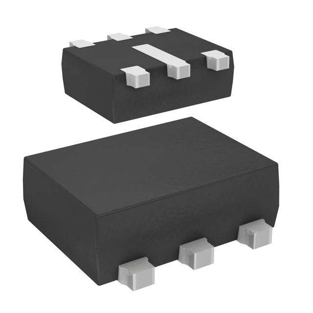
| 供应商器件封装 | 5-TSSOP |
| 其它名称 | 568-11079-1 |
| 包装 | 剪切带 (CT) |
| 商标 | NXP Semiconductors |
| 安装类型 | 表面贴装 |
| 安装风格 | SMD/SMT |
| 封装 | Reel |
| 封装/外壳 | 6-TSSOP(5 引线),SC-88A,SOT-353 |
| 封装/箱体 | SOT-353 |
| 工作温度 | -40°C ~ 125°C |
| 工厂包装数量 | 3000 |
| 最大工作温度 | + 125 C |
| 最小工作温度 | - 40 C |
| 栅极数量 | 1 Gate |
| 标准包装 | 1 |
| 特性 | - |
| 电压-电源 | 4.5 V ~ 5.5 V |
| 电流-输出高,低 | 2mA,2mA |
| 电流-静态(最大值) | 10µA |
| 电源电压-最大 | 5.5 V |
| 电源电压-最小 | 4.5 V |
| 电路数 | 1 |
| 输入/输出线数量 | 2 / 1 |
| 输入数 | 2 |
| 输入线路数量 | 2 |
| 输出线路数量 | 1 |
| 逻辑电平-低 | 0.8V |
| 逻辑电平-高 | 2V |
| 逻辑类型 | XOR(异或) |
| 逻辑系列 | HCT |
| 零件号别名 | 74HCT1G86GW-G |
| 高电平输出电流 | - 2 mA |


- 商务部:美国ITC正式对集成电路等产品启动337调查
- 曝三星4nm工艺存在良率问题 高通将骁龙8 Gen1或转产台积电
- 太阳诱电将投资9.5亿元在常州建新厂生产MLCC 预计2023年完工
- 英特尔发布欧洲新工厂建设计划 深化IDM 2.0 战略
- 台积电先进制程称霸业界 有大客户加持明年业绩稳了
- 达到5530亿美元!SIA预计今年全球半导体销售额将创下新高
- 英特尔拟将自动驾驶子公司Mobileye上市 估值或超500亿美元
- 三星加码芯片和SET,合并消费电子和移动部门,撤换高东真等 CEO
- 三星电子宣布重大人事变动 还合并消费电子和移动部门
- 海关总署:前11个月进口集成电路产品价值2.52万亿元 增长14.8%


PDF Datasheet 数据手册内容提取
74HC1G86; 74HCT1G86 2-input EXCLUSIVE-OR gate Rev. 04 — 20 July 2007 Product data sheet 1. General description 74HC1G86 and 74HCT1G86 are high-speed Si-gate CMOS devices. They provide a 2-input EXCLUSIVE-OR function. The HC device has CMOS input switching levels and supply voltage range 2 V to 6 V. The HCT device has TTL input switching levels and supply voltage range 4.5 V to 5.5 V. The standard output currents arehalf those of the 74HC/HCT86. 2. Features n Symmetrical output impedance n High noise immunity n Low power dissipation n Balanced propagation delays n SOT353-1 and SOT753 package options n Specified from-40 (cid:176)Cto+125 (cid:176)C 3. Ordering information Table 1. Ordering information Type number Package Temperature range Name Description Version 74HC1G86GW -40 (cid:176)C to +125 (cid:176)C TSSOP5 plastic thin shrink small outline package; SOT353-1 5leads; body width1.25mm 74HCT1G86GW 74HC1G86GV -40 (cid:176)C to +125 (cid:176)C SC-74A plastic surface-mounted package; 5 leads SOT753 74HCT1G86GV 4. Marking Table 2. Marking codes Type number Marking 74HC1G86GW HH 74HCT1G86GW TH 74HC1G86GV H86 74HCT1G86GV T86
74HC1G86; 74HCT1G86 Nexperia 2-input EXCLUSIVE-OR gate 5. Functional diagram B 1 Y A 4 1 = 1 2 4 2 mna038 mna039 Fig 1. Logic symbol Fig 2. IEC logic symbol B Y A mna040 Fig 3. Logic diagram 6. Pinning information 6.1 Pinning 74HC1G86 B 1 5 VCC A 2 GND 3 4 Y 001aaf055 Fig 4. Pin configuration 6.2 Pin description Table 3. Pin description Symbol Pin Description B 1 data input A 2 data input GND 3 ground (0 V) Y 4 data output V 5 supply voltage CC 74HC_HCT1G86_4 © Nexperia B.V. 2017. All rights reserved Product data sheet Rev. 04 — 20 July 2007 2 of 11
74HC1G86; 74HCT1G86 Nexperia 2-input EXCLUSIVE-OR gate 7. Functional description Table 4. Function table H = HIGH voltage level; L = LOW voltage level Inputs Output A B Y L L L L H H H L H H H L 8. Limiting values Table 5. Limiting values In accordance with the Absolute Maximum Rating System (IEC 60134). Voltages are referenced to GND (ground = 0 V).[1] Symbol Parameter Conditions Min Max Unit V supply voltage - 0.5 +7.0 V CC I input clamping current V <-0.5V or V >V + 0.5V - –20 mA IK I I CC I output clamping current V <-0.5V or V >V + 0.5V - –20 mA OK O O CC I output current -0.5 V < V <V +0.5V - –12.5 mA O O CC I supply current - 25 mA CC I ground current - 25 - mA GND T storage temperature - 65 +150 (cid:176)C stg P total power dissipation T =-40 (cid:176)Cto+125 (cid:176)C [2] - 200 mW tot amb [1] The input and output voltage ratings may be exceeded if the input and output current ratings are observed. [2] Above 55(cid:176)C the value ofP derates linearly with 2.5mW/K. tot 9. Recommended operating conditions Table 6. Recommended operating conditions Voltages are referenced to GND (ground = 0 V). Symbol Parameter Conditions 74HC1G86 74HCT1G86 Unit Min Typ Max Min Typ Max V supply voltage 2.0 5.0 6.0 4.5 5.0 5.5 V CC V input voltage 0 - V 0 - V V I CC CC V output voltage 0 - V 0 - V V O CC CC T ambient temperature -40 +25 +125 - 40 +25 +125 (cid:176)C amb Dt/DV input transition rise V = 2.0 V - - 625 - - - ns/V CC and fall rate V = 4.5 V - - 139 - - 139 ns/V CC V = 6.0 V - - 83 - - - ns/V CC 74HC_HCT1G86_4 © Nexperia B.V. 2017. All rights reserved Product data sheet Rev. 04 — 20 July 2007 3 of 11
74HC1G86; 74HCT1G86 Nexperia 2-input EXCLUSIVE-OR gate 10. Static characteristics Table 7. Static characteristics Voltages are referenced to GND (ground = 0 V). All typical values are measured at T =25(cid:176) C. amb Symbol Parameter Conditions - 40(cid:176)C to+85 (cid:176)C -40 (cid:176)C to+125 (cid:176)C Unit Min Typ Max Min Max For type 74HC1G86 V HIGH-level input V = 2.0 V 1.5 1.2 - 1.5 - V IH CC voltage V = 4.5 V 3.15 2.4 - 3.15 - V CC V = 6.0 V 4.2 3.2 - 4.2 - V CC V LOW-level input V = 2.0 V - 0.8 0.5 - 0.5 V IL CC voltage V = 4.5 V - 2.1 1.35 - 1.35 V CC V = 6.0 V - 2.8 1.8 - 1.8 V CC V HIGH-level output V = V or V OH I IH IL voltage I =-20 m A; V =2.0V 1.9 2.0 - 1.9 - V O CC I =-20 m A; V =4.5V 4.4 4.5 - 4.4 - V O CC I =-20 m A; V =6.0V 5.9 6.0 - 5.9 - V O CC I =-2.0mA; V =4.5V 4.13 4.32 - 3.7 - V O CC I =-2.6mA; V =6.0V 5.63 5.81 - 5.2 - V O CC V LOW-level output V = V or V OL I IH IL voltage I = 20m A; V =2.0V - 0 0.1 - 0.1 V O CC I = 20m A; V =4.5V - 0 0.1 - 0.1 V O CC I = 20m A; V =6.0V - 0 0.1 - 0.1 V O CC I = 2.0mA; V =4.5V - 0.15 0.33 - 0.4 V O CC I = 2.6mA; V =6.0V - 0.16 0.33 - 0.4 V O CC I input leakage current V =V orGND; V =6.0V - - 1.0 - 1.0 m A I I CC CC I supply current V =V orGND; I =0A; - - 10 - 20 m A CC I CC O V =6.0V CC C input capacitance - 1.5 - - - pF I For type 74HCT1G86 V HIGH-level input V = 4.5 V to 5.5 V 2.0 1.6 - 2.0 - V IH CC voltage V LOW-level input V = 4.5 V to 5.5 V - 1.2 0.8 - 0.8 V IL CC voltage V HIGH-level output V = V or V OH I IH IL voltage I =-20 m A; V =4.5V 4.4 4.5 - 4.4 - V O CC I =-2.0mA; V =4.5V 4.13 4.32 - 3.7 - V O CC V LOW-level output V = V or V OL I IH IL voltage I = 20m A; V =4.5V - 0 0.1 - 0.1 V O CC I = 2.0mA; V =4.5V - 0.15 0.33 - 0.4 V O CC I input leakage current V =V orGND; V =5.5V - - 1.0 - 1.0 m A I I CC CC 74HC_HCT1G86_4 © Nexperia B.V. 2017. All rights reserved Product data sheet Rev. 04 — 20 July 2007 4 of 11
74HC1G86; 74HCT1G86 Nexperia 2-input EXCLUSIVE-OR gate Table 7. Static characteristics …continued Voltages are referenced to GND (ground = 0 V). All typical values are measured at T =25(cid:176) C. amb Symbol Parameter Conditions - 40(cid:176)C to+85 (cid:176)C -40 (cid:176)C to+125 (cid:176)C Unit Min Typ Max Min Max I supply current V =V orGND; I =0A; - - 10 - 20 m A CC I CC O V =5.5V CC DI additional supply per input; V =4.5Vto5.5V; - - 500 - 850 m A CC CC current V =V - 2.1V; I =0A I CC O C input capacitance - 1.5 - - - pF I 11. Dynamic characteristics Table 8. Dynamic characteristics GND = 0 V; t = t£ 6.0 ns; All typical values are measured at T =25(cid:176) C. For test circuit seeFigure6 r f amb Symbol Parameter Conditions -40 (cid:176)C to+85 (cid:176)C -40 (cid:176)C to+125 (cid:176)C Unit Min Typ Max Min Max For type 74HC1G86 t propagation delay Aand B toY; seeFigure5 [1] pd V = 2.0 V; C =50pF - 22 115 - 135 ns CC L V = 4.5 V; C =50pF - 11 23 - 27 ns CC L V = 5.0 V; C =15pF - 9 - - - ns CC L V = 6.0 V; C =50pF - 9 20 - 23 ns CC L C power dissipation V =GNDtoV [2] - 23 - - - pF PD I CC capacitance For type 74HCT1G86 t propagation delay Aand B toY; seeFigure5 [1] pd V = 4.5 V; C =50pF - 13 23 - 27 ns CC L V = 5.0 V; C =15pF - 10 - - - ns CC L C power dissipation V =GNDtoV - 1.5V [2] - 23 - - - pF PD I CC capacitance [1] t is the same as t and t . pd PLH PHL [2] C is used to determine the dynamic power dissipation P (mW). PD D P =C · V 2· f +(cid:229) (C · V 2· f )where: D PD CC i L CC o f =input frequency in MHz i f =output frequency in MHz o C =output load capacitance in pF L V =supply voltage in Volts CC (cid:229) (C · V 2· f ) = sum of outputs L CC o 74HC_HCT1G86_4 © Nexperia B.V. 2017. All rights reserved Product data sheet Rev. 04 — 20 July 2007 5 of 11
74HC1G86; 74HCT1G86 Nexperia 2-input EXCLUSIVE-OR gate 12. Waveforms A, B input VM tPHL tPLH Y output VM mna041 For 74HC1G86: V =0.5· V ; V =GNDtoV . M CC I CC For 74HCT1G86:V =1.3V; V =GNDto3.0V. M I Fig 5. The input (AandB) to output (Y) propagation delays VCC VI VO PULSE DUT GENERATOR RT C50L pF mna034 Test data is given inTable8. Definitions for test circuit: C = Load capacitance including jig and probe capacitance. L R = Termination resistance should be equal to output impedance Z of the pulse generator. T o Fig 6. Load circuitry for switching times 74HC_HCT1G86_4 © Nexperia B.V. 2017. All rights reserved Product data sheet Rev. 04 — 20 July 2007 6 of 11
74HC1G86; 74HCT1G86 Nexperia 2-input EXCLUSIVE-OR gate 13. Package outline TSSOP5: plastic thin shrink small outline package; 5 leads; body width 1.25 mm SOT353-1 D E A X c y HE v M A Z 5 4 A2 A A1 (A3) q 1 3 Lp L e w M bp e1 detail X 0 1.5 3 mm scale DIMENSIONS (mm are the original dimensions) UNIT mAax. A1 A2 A3 bp c D(1) E(1) e e1 HE L Lp v w y Z(1) q mm 1.1 0.1 1.0 0.15 0.30 0.25 2.25 1.35 0.65 1.3 2.25 0.425 0.46 0.3 0.1 0.1 0.60 7(cid:176) 0 0.8 0.15 0.08 1.85 1.15 2.0 0.21 0.15 0(cid:176) Note 1. Plastic or metal protrusions of 0.15 mm maximum per side are not included. OUTLINE REFERENCES EUROPEAN ISSUE DATE VERSION IEC JEDEC JEITA PROJECTION 00-09-01 SOT353-1 MO-203 SC-88A 03-02-19 Fig 7. Package outline SOT353-1 (TSSOP5) 74HC_HCT1G86_4 © Nexperia B.V. 2017. All rights reserved Product data sheet Rev. 04 — 20 July 2007 7 of 11
74HC1G86; 74HCT1G86 Nexperia 2-input EXCLUSIVE-OR gate Plastic surface-mounted package; 5 leads SOT753 D B E A X y HE v M A 5 4 Q A A1 c 1 2 3 Lp detail X e bp w M B 0 1 2 mm scale DIMENSIONS (mm are the original dimensions) UNIT A A1 bp c D E e HE Lp Q v w y 1.1 0.100 0.40 0.26 3.1 1.7 3.0 0.6 0.33 mm 0.95 0.2 0.2 0.1 0.9 0.013 0.25 0.10 2.7 1.3 2.5 0.2 0.23 OUTLINE REFERENCES EUROPEAN ISSUE DATE VERSION IEC JEDEC JEITA PROJECTION 02-04-16 SOT753 SC-74A 06-03-16 Fig 8. Package outline SOT753 (SC-74A) 74HC_HCT1G86_4 © Nexperia B.V. 2017. All rights reserved Product data sheet Rev. 04 — 20 July 2007 8 of 11
74HC1G86; 74HCT1G86 Nexperia 2-input EXCLUSIVE-OR gate 14. Abbreviations Table 9. Abbreviations Acronym Description DUT Device Under Test TTL Transistor-Transistor Logic 15. Revision history Table 10. Revision history Document ID Release date Data sheet status Change notice Supersedes 74HC_HCT1G86_4 20070720 Product data sheet - 74HC_HCT1G86_3 Modifications: • The format of this data sheet has been redesigned to comply with the new identity guidelines of NXP Semiconductors. • Legal texts have been adapted to the new company name where appropriate. • Package SOT353 changed to SOT353-1 inTable1 andFigure7. • Quick Reference Data and Soldering sections removed. • Section 2 “Features” updated. 74HC_HCT1G86_3 20020515 Product specification - 74HC_HCT1G86_2 74HC_HCT1G86_2 20010406 Product specification - 74HC_HCT1G86_1 74HC_HCT1G86_1 19980805 Product specification - - 74HC_HCT1G86_4 © Nexperia B.V. 2017. All rights reserved Product data sheet Rev. 04 — 20 July 2007 9 of 11
74HC1G86; 74HCT1G86 Nexperia 2-input EXCLUSIVE-OR gate 16. Legal information 16.1 Data sheet status Document status[1][2] Product status[3] Definition Objective [short] data sheet Development This document contains data from the objective specification for product development. Preliminary [short] data sheet Qualification This document contains data from the preliminary specification. Product [short] data sheet Production This document contains the product specification. [1] Please consult the most recently issued document before initiating or completing a design. [2] The term ‘short data sheet’ is explained in section “Definitions”. [3] Theproductstatusofdevice(s)describedinthisdocumentmayhavechangedsincethisdocumentwaspublishedandmaydifferincaseofmultipledevices.Thelatestproductstatus information is available on the Internet at URLhttp://www.nexperia.com. 16.2 Definitions malfunctionofaNexperiaproductcanreasonablybeexpectedto result in personal injury, death or severe property or environmental damage. Nexperia accepts no liability for inclusion and/or use of Nexperia Draft —The document is a draft version only. The content is still under products in such equipment or applications and therefore internal review and subject to formal approval, which may result in such inclusion and/or use is at the customer’s own risk. modifications or additions. Nexperia does not give any representations or warranties as to the accuracy or completeness of Applications —Applications that are described herein for any of these informationincludedhereinandshallhavenoliabilityfortheconsequencesof products are for illustrative purposes only. Nexperia makes no use of such information. representation or warranty that such applications will be suitable for the specified use without further testing or modification. Short data sheet —A short data sheet is an extract from a full data sheet withthesameproducttypenumber(s)andtitle.Ashortdatasheetisintended Limiting values —Stress above one or more limiting values (as defined in forquickreferenceonlyandshouldnotbereliedupontocontaindetailedand theAbsoluteMaximumRatingsSystemofIEC60134)maycausepermanent full information. For detailed and full information see the relevant full data damagetothedevice.Limitingvaluesarestressratingsonlyandoperationof sheet, which is available on request via the local Nexperia sales the device at these or any other conditions above those given in the office. In case of any inconsistency or conflict with the short data sheet, the Characteristics sections of this document is not implied. Exposure to limiting full data sheet shall prevail. values for extended periods may affect device reliability. Terms and conditions of sale —Nexperia products are sold 16.3 Disclaimers subjecttothegeneraltermsandconditionsofcommercialsale,aspublished athttp://www.nexperia.com/profile/terms, including those pertaining to warranty, intellectual property rights infringement and limitation of liability, unless General —Information in this document is believed to be accurate and explicitly otherwise agreed to in writing by Nexperia. In case of reliable.However,Nexperiadoesnotgiveanyrepresentationsor any inconsistency or conflict between information in this document and such warranties,expressedorimplied,astotheaccuracyorcompletenessofsuch terms and conditions, the latter will prevail. information and shall have no liability for the consequences of use of such No offer to sell or license —Nothing in this document may be interpreted information. or construed as an offer to sell products that is open for acceptance or the Right to make changes —Nexperiareservestherighttomake grant,conveyanceorimplicationofanylicenseunderanycopyrights,patents changes to information published in this document, including without or other industrial or intellectual property rights. limitation specifications and product descriptions, at any time and without notice.Thisdocumentsupersedesandreplacesallinformationsuppliedprior to the publication hereof. 16.4 Trademarks Suitability for use —Nexperia products are not designed, Notice:Allreferencedbrands,productnames,servicenamesandtrademarks authorized or warranted to be suitable for use in medical, military, aircraft, are the property of their respective owners. space or life support equipment, nor in applications where failure or 17. Contact information For additional information, please visit:http://www.nexperia.com For sales office addresses, send an email to:salesaddresses@nexperia.com 74HC_HCT1G86_4 © Nexperia B.V. 2017. All rights reserved Product data sheet Rev. 04 — 20 July 2007 10 of 11
74HC1G86; 74HCT1G86 Nexperia 2-input EXCLUSIVE-OR gate 18. Contents 1 General description. . . . . . . . . . . . . . . . . . . . . . 1 2 Features . . . . . . . . . . . . . . . . . . . . . . . . . . . . . . . 1 3 Ordering information. . . . . . . . . . . . . . . . . . . . . 1 4 Marking. . . . . . . . . . . . . . . . . . . . . . . . . . . . . . . . 1 5 Functional diagram . . . . . . . . . . . . . . . . . . . . . . 2 6 Pinning information. . . . . . . . . . . . . . . . . . . . . . 2 6.1 Pinning . . . . . . . . . . . . . . . . . . . . . . . . . . . . . . . 2 6.2 Pin description . . . . . . . . . . . . . . . . . . . . . . . . . 2 7 Functional description . . . . . . . . . . . . . . . . . . . 3 8 Limiting values. . . . . . . . . . . . . . . . . . . . . . . . . . 3 9 Recommended operating conditions. . . . . . . . 3 10 Static characteristics. . . . . . . . . . . . . . . . . . . . . 4 11 Dynamic characteristics . . . . . . . . . . . . . . . . . . 5 12 Waveforms . . . . . . . . . . . . . . . . . . . . . . . . . . . . . 6 13 Package outline . . . . . . . . . . . . . . . . . . . . . . . . . 7 14 Abbreviations. . . . . . . . . . . . . . . . . . . . . . . . . . . 9 15 Revision history. . . . . . . . . . . . . . . . . . . . . . . . . 9 16 Legal information. . . . . . . . . . . . . . . . . . . . . . . 10 16.1 Data sheet status . . . . . . . . . . . . . . . . . . . . . . 10 16.2 Definitions. . . . . . . . . . . . . . . . . . . . . . . . . . . . 10 16.3 Disclaimers. . . . . . . . . . . . . . . . . . . . . . . . . . . 10 16.4 Trademarks. . . . . . . . . . . . . . . . . . . . . . . . . . . 10 17 Contact information. . . . . . . . . . . . . . . . . . . . . 10 18 Contents. . . . . . . . . . . . . . . . . . . . . . . . . . . . . . 11 © Nexperia B.V. 2017. All rights reserved For more information, please visit: http://www.nexperia.com For sales office addresses, please send an email to: salesaddresses@nexperia.com Date of release: 20 July 2007