ICGOO在线商城 > 74AUP3G3404GDH

 Datasheet下载
- 型号: 74AUP3G3404GDH
- 制造商: NXP Semiconductors
- 库位|库存: xxxx|xxxx
- 要求:
| 数量阶梯 | 香港交货 | 国内含税 |
| +xxxx | $xxxx | ¥xxxx |
查看当月历史价格
查看今年历史价格
74AUP3G3404GDH产品简介:
ICGOO电子元器件商城为您提供74AUP3G3404GDH由NXP Semiconductors设计生产,在icgoo商城现货销售,并且可以通过原厂、代理商等渠道进行代购。 提供74AUP3G3404GDH价格参考以及NXP Semiconductors74AUP3G3404GDH封装/规格参数等产品信息。 你可以下载74AUP3G3404GDH参考资料、Datasheet数据手册功能说明书, 资料中有74AUP3G3404GDH详细功能的应用电路图电压和使用方法及教程。
| 参数 | 数值 |
| 产品目录 | 集成电路 (IC) |
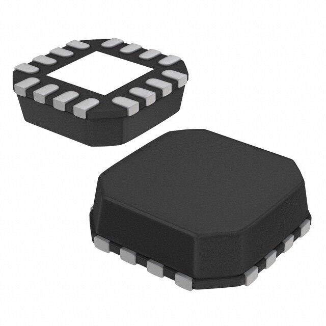
| 描述 | IC DUAL BUFFER SGL INVERT 8XSON |
| 产品分类 | |
| 品牌 | NXP Semiconductors |
| 数据手册 | |
| 产品图片 | |
| 产品型号 | 74AUP3G3404GDH |
| rohs | 无铅 / 符合限制有害物质指令(RoHS)规范要求 |
| 产品系列 | 74AUP |
| 供应商器件封装 | 8-XSON,SOT996-2 (2x3) |
| 其它名称 | 568-11393-1 |
| 包装 | 剪切带 (CT) |
| 安装类型 | 表面贴装 |
| 封装/外壳 | 8-XFDFN |
| 工作温度 | -40°C ~ 125°C |
| 施密特触发器输入 | 是 |
| 标准包装 | 1 |
| 电压-电源 | 0.8 V ~ 3.6 V |
| 电流-输出高,低 | 4mA,4mA |
| 电路数 | 3 |
| 输入数 | 3 输入(2,1) |
| 输出类型 | 单端 |
| 逻辑类型 | 缓冲器/逆变器 |


- 商务部:美国ITC正式对集成电路等产品启动337调查
- 曝三星4nm工艺存在良率问题 高通将骁龙8 Gen1或转产台积电
- 太阳诱电将投资9.5亿元在常州建新厂生产MLCC 预计2023年完工
- 英特尔发布欧洲新工厂建设计划 深化IDM 2.0 战略
- 台积电先进制程称霸业界 有大客户加持明年业绩稳了
- 达到5530亿美元!SIA预计今年全球半导体销售额将创下新高
- 英特尔拟将自动驾驶子公司Mobileye上市 估值或超500亿美元
- 三星加码芯片和SET,合并消费电子和移动部门,撤换高东真等 CEO
- 三星电子宣布重大人事变动 还合并消费电子和移动部门
- 海关总署:前11个月进口集成电路产品价值2.52万亿元 增长14.8%


PDF Datasheet 数据手册内容提取
74AUP3G3404 Low-power dual buffer and single inverter Rev. 2 — 26 April 2019 Product data sheet 1. General description The 74AUP3G3404 is a dual buffer and single inverter. Schmitt trigger action at all inputs makes the circuit tolerant of slower input rise and fall times across the entire V range from 0.8 V to 3.6 V. CC This device ensures a very low static and dynamic power consumption across the entire V range CC from 0.8 V to 3.6 V. This device is fully specified for partial Power-down applications using I . The I circuitry OFF OFF disables the output, preventing a damaging backflow current through the device when it is powered down. 2. Features and benefits • Wide supply voltage range from 0.8 V to 3.6 V • High noise immunity • Complies with JEDEC standards: • JESD8-12 (0.8 V to 1.3 V) • JESD8-11 (0.9 V to 1.65 V) • JESD8-7 (1.2 V to 1.95 V) • JESD8-5 (1.8 V to 2.7 V) • JESD8-B (2.7 V to 3.6 V) • ESD protection: • HBM JESD22-A114F Class 3A exceeds 5000 V • MM JESD22-A115-A exceeds 200 V • CDM JESD22-C101E exceeds 1000 V • Low static power consumption; I = 0.9 μA (maximum) CC • Latch-up performance exceeds 100 mA per JESD 78B Class II • Inputs accept voltages up to 3.6 V • Low noise overshoot and undershoot < 10 % of V CC • I circuitry provides partial Power-down mode operation OFF • Multiple package options • Specified from -40 °C to +85 °C and -40 °C to +125 °C
Nexperia 74AUP3G3404 Low-power dual buffer and single inverter 3. Ordering information Table 1. Ordering information Type number Package Temperature range Name Description Version 74AUP3G3404DC -40 °C to +125 °C VSSOP8 plastic very thin shrink small outline package; SOT765-1 8 leads; body width 2.3 mm 74AUP3G3404GT -40 °C to +125 °C XSON8 plastic extremely thin small outline package; SOT833-1 no leads; 8 terminals; body 1 x 1.95 x 0.5 mm 74AUP3G3404GF -40 °C to +125 °C XSON8 extremely thin small outline package; no leads; SOT1089 8 terminals; body 1.35 x 1 x 0.5 mm 74AUP3G3404GM -40 °C to +125 °C XQFN8 plastic, extremely thin quad flat package; no leads; SOT902-2 8 terminals; body 1.6 x 1.6 x 0.5 mm 74AUP3G3404GN -40 °C to +125 °C XSON8 extremely thin small outline package; no leads; SOT1116 8 terminals; body 1.2 x 1.0 x 0.35 mm 74AUP3G3404GS -40 °C to +125 °C XSON8 extremely thin small outline package; no leads; SOT1203 8 terminals; body 1.35 x 1.0 x 0.35 mm 4. Marking Table 2. Marking codes Type number Marking code[1] 74AUP3G3404DC aZ 74AUP3G3404GT aZ 74AUP3G3404GF aZ 74AUP3G3404GM aZ 74AUP3G3404GN aZ 74AUP3G3404GS aZ [1] The pin 1 indicator is located on the lower left corner of the device, below the marking code. 5. Functional diagram 1 1A 1Y 1 1A 1Y 2A 2Y 2A 2Y 3A 3Y 1 3A 3Y aaa-005904 aaa-005905 aaa-005906 Fig. 1. Logic symbol Fig. 2. IEC logic symbol Fig. 3. Logic diagram 74AUP3G3404 All information provided in this document is subject to legal disclaimers. © Nexperia B.V. 2019. All rights reserved Product data sheet Rev. 2 — 26 April 2019 2 / 19
Nexperia 74AUP3G3404 Low-power dual buffer and single inverter 6. Pinning information 6.1. Pinning 74AUP3G3404 1A 1 8 VCC 3Y 2 7 1Y 74AUP3G3404 2A 3 6 3A 1A 1 8 VCC 3Y 2 7 1Y GND 4 5 2Y 2A 3 6 3A aaa-005907 GND 4 5 2Y Transparent top view aaa-005908 Fig. 5. Pin configuration SOT833-1, SOT1089, SOT1116 Fig. 4. Pin configuration SOT765-1 (VSSOP8) and SOT1203 (XSON8) 74AUP3G3404 terminal 1 C C index area V 1Y 1 8 7 1A 3A 2 6 3Y 2Y 3 5 2A 4 ND aaa-005910 G Transparent top view Fig. 6. Pin configuration SOT902-2 (XQFN8) 6.2. Pin description Table 3. Pin description Symbol Pin Description SOT765-1, SOT833-1, SOT1089, SOT1116 and SOT902-2 SOT1203 1A, 2A, 3A 1, 3, 6 7, 5, 2 data input 1Y, 2Y, 3Y 7, 5, 2 1, 3, 6 data output GND 4 4 ground (0 V) V 8 8 supply voltage CC 74AUP3G3404 All information provided in this document is subject to legal disclaimers. © Nexperia B.V. 2019. All rights reserved Product data sheet Rev. 2 — 26 April 2019 3 / 19
Nexperia 74AUP3G3404 Low-power dual buffer and single inverter 7. Functional description Table 4. Function table H = HIGH voltage level; L = LOW voltage level. Input Output 1A, 3A 1Y, 3Y L L H H Table 5. Function table H = HIGH voltage level; L = LOW voltage level. Input Output 2A 2Y L H H L 8. Limiting values Table 6. Limiting values In accordance with the Absolute Maximum Rating System (IEC 60134). Voltages are referenced to GND (ground = 0 V). Symbol Parameter Conditions Min Max Unit V supply voltage -0.5 +4.6 V CC I input clamping current V < 0 V -50 - mA IK I V input voltage [1] -0.5 +4.6 V I I output clamping current V < 0 V -50 - mA OK O V output voltage Active mode and Power-down mode [1] -0.5 +4.6 V O I output current V = 0 V to V - ±20 mA O O CC I supply current - 50 mA CC I ground current -50 - mA GND T storage temperature -65 +150 °C stg P total power dissipation T = -40 °C to +125 °C [2] - 250 mW tot amb [1] The minimum input and output voltage ratings may be exceeded if the input and output current ratings are observed. [2] For VSSOP8 packages: above 110 °C the value of Ptot derates linearly with 8.0 mW/K. For XSON8 and XQFN8 packages: above 118 °C the value of Ptot derates linearly with 7.8 mW/K. 9. Recommended operating conditions Table 7. Operating conditions Symbol Parameter Conditions Min Max Unit V supply voltage 0.8 3.6 V CC V input voltage 0 3.6 V I V output voltage Active mode 0 V V O CC Power-down mode; V = 0 V 0 3.6 V CC T ambient temperature -40 +125 °C amb Δt/ΔV input transition rise and fall rate V = 0.8 V to 3.6 V - 200 ns/V CC 74AUP3G3404 All information provided in this document is subject to legal disclaimers. © Nexperia B.V. 2019. All rights reserved Product data sheet Rev. 2 — 26 April 2019 4 / 19
Nexperia 74AUP3G3404 Low-power dual buffer and single inverter 10. Static characteristics Table 8. Static characteristics At recommended operating conditions; voltages are referenced to GND (ground = 0 V). Symbol Parameter Conditions Min Typ Max Unit T = 25 °C amb V HIGH-level input voltage V = 0.8 V 0.70V - - V IH CC CC V = 0.9 V to 1.95 V 0.65V - - V CC CC V = 2.3 V to 2.7 V 1.6 - - V CC V = 3.0 V to 3.6 V 2.0 - - V CC V LOW-level input voltage V = 0.8 V - - 0.30V V IL CC CC V = 0.9 V to 1.95 V - - 0.35V V CC CC V = 2.3 V to 2.7 V - - 0.7 V CC V = 3.0 V to 3.6 V - - 0.9 V CC V HIGH-level output voltage V = V or V OH I IH IL I = -20 μA; V = 0.8 V to 3.6 V V - 0.1 - - V O CC CC I = -1.1 mA; V = 1.1 V 0.75V - - V O CC CC I = -1.7 mA; V = 1.4 V 1.11 - - V O CC I = -1.9 mA; V = 1.65 V 1.32 - - V O CC I = -2.3 mA; V = 2.3 V 2.05 - - V O CC I = -3.1 mA; V = 2.3 V 1.9 - - V O CC I = -2.7 mA; V = 3.0 V 2.72 - - V O CC I = -4.0 mA; V = 3.0 V 2.6 - - V O CC V LOW-level output voltage V = V or V OL I IH IL I = 20 μA; V = 0.8 V to 3.6 V - - 0.1 V O CC I = 1.1 mA; V = 1.1 V - - 0.3V V O CC CC I = 1.7 mA; V = 1.4 V - - 0.31 V O CC I = 1.9 mA; V = 1.65 V - - 0.31 V O CC I = 2.3 mA; V = 2.3 V - - 0.31 V O CC I = 3.1 mA; V = 2.3 V - - 0.44 V O CC I = 2.7 mA; V = 3.0 V - - 0.31 V O CC I = 4.0 mA; V = 3.0 V - - 0.44 V O CC I input leakage current V = GND to 3.6 V; V = 0 V to 3.6 V - - ±0.1 μA I I CC I power-off leakage current V or V = 0 V to 3.6 V; V = 0 V - - ±0.2 μA OFF I O CC ΔI additional power-off V or V = 0 V to 3.6 V; - - ±0.2 μA OFF I O leakage current V = 0 V to 0.2 V CC I supply current V = GND or V ; I = 0 A; - - 0.5 μA CC I CC O V = 0.8 V to 3.6 V CC ΔI additional supply current V = V - 0.6 V; I = 0 A; - - 40 μA CC I CC O V = 3.3 V CC C input capacitance V = 0 V to 3.6 V; V = GND or V - 1.0 - pF I CC I CC C output capacitance V = GND; V = 0 V - 1.8 - pF O O CC 74AUP3G3404 All information provided in this document is subject to legal disclaimers. © Nexperia B.V. 2019. All rights reserved Product data sheet Rev. 2 — 26 April 2019 5 / 19
Nexperia 74AUP3G3404 Low-power dual buffer and single inverter Symbol Parameter Conditions Min Typ Max Unit T = -40 °C to +85 °C amb V HIGH-level input voltage V = 0.8 V 0.70V - - V IH CC CC V = 0.9 V to 1.95 V 0.65V - - V CC CC V = 2.3 V to 2.7 V 1.6 - - V CC V = 3.0 V to 3.6 V 2.0 - - V CC V LOW-level input voltage V = 0.8 V - - 0.30V V IL CC CC V = 0.9 V to 1.95 V - - 0.35V V CC CC V = 2.3 V to 2.7 V - - 0.7 V CC V = 3.0 V to 3.6 V - - 0.9 V CC V HIGH-level output voltage V = V or V OH I IH IL I = -20 μA; V = 0.8 V to 3.6 V V - 0.1 - - V O CC CC I = -1.1 mA; V = 1.1 V 0.7V - - V O CC CC I = -1.7 mA; V = 1.4 V 1.03 - - V O CC I = -1.9 mA; V = 1.65 V 1.30 - - V O CC I = -2.3 mA; V = 2.3 V 1.97 - - V O CC I = -3.1 mA; V = 2.3 V 1.85 - - V O CC I = -2.7 mA; V = 3.0 V 2.67 - - V O CC I = -4.0 mA; V = 3.0 V 2.55 - - V O CC V LOW-level output voltage V = V or V OL I IH IL I = 20 μA; V = 0.8 V to 3.6 V - - 0.1 V O CC I = 1.1 mA; V = 1.1 V - - 0.3V V O CC CC I = 1.7 mA; V = 1.4 V - - 0.37 V O CC I = 1.9 mA; V = 1.65 V - - 0.35 V O CC I = 2.3 mA; V = 2.3 V - - 0.33 V O CC I = 3.1 mA; V = 2.3 V - - 0.45 V O CC I = 2.7 mA; V = 3.0 V - - 0.33 V O CC I = 4.0 mA; V = 3.0 V - - 0.45 V O CC I input leakage current V = GND to 3.6 V; V = 0 V to 3.6 V - - ±0.5 μA I I CC I power-off leakage current V or V = 0 V to 3.6 V; V = 0 V - - ±0.5 μA OFF I O CC ΔI additional power-off V or V = 0 V to 3.6 V; - - ±0.6 μA OFF I O leakage current V = 0 V to 0.2 V CC I supply current V = GND or V ; I = 0 A; - - 0.9 μA CC I CC O V = 0.8 V to 3.6 V CC ΔI additional supply current V = V - 0.6 V; I = 0 A; - - 50 μA CC I CC O V = 3.3 V CC 74AUP3G3404 All information provided in this document is subject to legal disclaimers. © Nexperia B.V. 2019. All rights reserved Product data sheet Rev. 2 — 26 April 2019 6 / 19
Nexperia 74AUP3G3404 Low-power dual buffer and single inverter Symbol Parameter Conditions Min Typ Max Unit T = -40 °C to +125 °C amb V HIGH-level input voltage V = 0.8 V 0.75V - - V IH CC CC V = 0.9 V to 1.95 V 0.70V - - V CC CC V = 2.3 V to 2.7 V 1.6 - - V CC V = 3.0 V to 3.6 V 2.0 - - V CC V LOW-level input voltage V = 0.8 V - - 0.25V V IL CC CC V = 0.9 V to 1.95 V - - 0.30V V CC CC V = 2.3 V to 2.7 V - - 0.7 V CC V = 3.0 V to 3.6 V - - 0.9 V CC V HIGH-level output voltage V = V or V OH I IH IL I = -20 μA; V = 0.8 V to 3.6 V V - 0.11 - - V O CC CC I = -1.1 mA; V = 1.1 V 0.6V - - V O CC CC I = -1.7 mA; V = 1.4 V 0.93 - - V O CC I = -1.9 mA; V = 1.65 V 1.17 - - V O CC I = -2.3 mA; V = 2.3 V 1.77 - - V O CC I = -3.1 mA; V = 2.3 V 1.67 - - V O CC I = -2.7 mA; V = 3.0 V 2.40 - - V O CC I = -4.0 mA; V = 3.0 V 2.30 - - V O CC V LOW-level output voltage V = V or V OL I IH IL I = 20 μA; V = 0.8 V to 3.6 V - - 0.11 V O CC I = 1.1 mA; V = 1.1 V - - 0.33V V O CC CC I = 1.7 mA; V = 1.4 V - - 0.41 V O CC I = 1.9 mA; V = 1.65 V - - 0.39 V O CC I = 2.3 mA; V = 2.3 V - - 0.36 V O CC I = 3.1 mA; V = 2.3 V - - 0.50 V O CC I = 2.7 mA; V = 3.0 V - - 0.36 V O CC I = 4.0 mA; V = 3.0 V - - 0.50 V O CC I input leakage current V = GND to 3.6 V; V = 0 V to 3.6 V - - ±0.75 μA I I CC I power-off leakage current V or V = 0 V to 3.6 V; V = 0 V - - ±0.75 μA OFF I O CC ΔI additional power-off V or V = 0 V to 3.6 V; - - ±0.75 μA OFF I O leakage current V = 0 V to 0.2 V CC I supply current V = GND or V ; I = 0 A; - - 1.4 μA CC I CC O V = 0.8 V to 3.6 V CC ΔI additional supply current V = V - 0.6 V; I = 0 A; - - 75 μA CC I CC O V = 3.3 V CC 74AUP3G3404 All information provided in this document is subject to legal disclaimers. © Nexperia B.V. 2019. All rights reserved Product data sheet Rev. 2 — 26 April 2019 7 / 19
Nexperia 74AUP3G3404 Low-power dual buffer and single inverter 11. Dynamic characteristics Table 9. Dynamic characteristics Voltages are referenced to GND (ground = 0 V); for test circuit see Fig. 8. Symbol Parameter Conditions 25 °C -40 °C to +125 °C Unit Min Typ[1] Max Min Max Max (85 °C) (125 °C) C = 5 pF L t propagation delay nA to nY; see Fig. 7 [2] pd V = 0.8 V - 16.0 - - - - ns CC V = 1.1 V to 1.3 V 2.4 5.0 10.3 2.0 11.4 12.6 ns CC V = 1.4 V to 1.6 V 1.8 3.6 6.4 1.6 7.4 8.2 ns CC V = 1.65 V to 1.95 V 1.5 2.9 5.0 1.4 5.9 6.5 ns CC V = 2.3 V to 2.7 V 1.2 2.4 3.9 1.1 4.5 5.0 ns CC V = 3.0 V to 3.6 V 1.1 2.1 3.2 1.0 3.9 4.3 ns CC C = 10 pF L t propagation delay nA to nY; see Fig. 7 [2] pd V = 0.8 V - 19.8 - - - - ns CC V = 1.1 V to 1.3 V 2.8 5.9 12.2 2.3 13.7 15.1 ns CC V = 1.4 V to 1.6 V 2.3 4.2 7.5 1.9 8.7 9.6 ns CC V = 1.65 V to 1.95 V 2.0 3.5 5.9 1.7 7.0 7.7 ns CC V = 2.3 V to 2.7 V 1.7 2.9 4.6 1.5 5.4 6.0 ns CC V = 3.0 V to 3.6 V 1.6 2.7 3.8 1.4 4.5 5.1 ns CC C = 15 pF L t propagation delay nA to nY; see Fig. 7 [2] pd V = 0.8 V - 23.3 - - - - ns CC V = 1.1 V to 1.3 V 3.2 6.7 13.0 2.6 15.8 17.4 ns CC V = 1.4 V to 1.6 V 2.6 4.7 8.6 2.2 10.0 11.0 ns CC V = 1.65 V to 1.95 V 2.3 4.0 6.7 2.0 8.0 8.8 ns CC V = 2.3 V to 2.7 V 2.1 3.3 5.1 1.8 6.1 6.8 ns CC V = 3.0 V to 3.6 V 2.0 3.1 4.2 1.6 5.0 5.5 ns CC C = 30 pF L t propagation delay nA to nY; see Fig. 7 [2] pd V = 0.8 V - 33.6 - - - - ns CC V = 1.1 V to 1.3 V 4.4 8.9 16.3 3.6 19.0 20.9 ns CC V = 1.4 V to 1.6 V 3.6 6.3 10.8 3.2 12.9 14.2 ns CC V = 1.65 V to 1.95 V 3.2 5.3 9.0 2.9 10.5 11.6 ns CC V = 2.3 V to 2.7 V 2.9 4.5 6.5 2.6 7.6 8.5 ns CC V = 3.0 V to 3.6 V 2.9 4.2 5.6 2.5 6.2 7.2 ns CC 74AUP3G3404 All information provided in this document is subject to legal disclaimers. © Nexperia B.V. 2019. All rights reserved Product data sheet Rev. 2 — 26 April 2019 8 / 19
Nexperia 74AUP3G3404 Low-power dual buffer and single inverter Symbol Parameter Conditions 25 °C -40 °C to +125 °C Unit Min Typ[1] Max Min Max Max (85 °C) (125 °C) C = 5 pF, 10 pF, 15 pF and 30 pF L C power dissipation f = 1 MHz; V = GND to V [3][4] PD i I CC capacitance V = 0.8 V - 2.5 - - - - pF CC V = 1.1 V to 1.3 V - 2.7 - - - - pF CC V = 1.4 V to 1.6 V - 2.8 - - - - pF CC V = 1.65 V to 1.95 V - 3.0 - - - - pF CC V = 2.3 V to 2.7 V - 3.5 - - - - pF CC V = 3.0 V to 3.6 V - 4.0 - - - - pF CC [1] All typical values are measured at nominal VCC. [2] tpd is the same as tPLH and tPHL. [3] All specified values are the average typical values over all stated loads. [4] CPD is used to determine the dynamic power dissipation (PD in μW). PD = CPD x VCC2 x fi x N + Σ(CL x VCC2 x fo) where: fi = input frequency in MHz; fo = output frequency in MHz; CL = load capacitance in pF; VCC = supply voltage in V; N = number of inputs switching; Σ(CL x VCC2 x fo) = sum of the outputs. 11.1. Waveforms and test circuit VI VI 1A, 3A input VM VM 2A input VM VM GND GND tPLH tPHL tPHL tPLH VOH VOH 1Y, 3Y output VM VM 2Y output VM VM VOL VOL aaa-005911 Measurement points are given in Table 10. Logic levels: V and V are typical output voltage levels that occur with the output load. OL OH Fig. 7. The data input 1A to output 1Y, input 2A to output 2Y and input 3A to output 3Y propagation delays Table 10. Measurement points Supply voltage Output Input V V V V t = t CC M M I r f 0.8 V to 3.6 V 0.5V 0.5V V ≤ 3.0 ns CC CC CC 74AUP3G3404 All information provided in this document is subject to legal disclaimers. © Nexperia B.V. 2019. All rights reserved Product data sheet Rev. 2 — 26 April 2019 9 / 19
Nexperia 74AUP3G3404 Low-power dual buffer and single inverter VCC VEXT 5 kΩ VI VO G DUT RT CL RL 001aac521 Test data is given in Table 11. Definitions for test circuit: R = Load resistance. L C = Load capacitance including jig and probe capacitance. L R = Termination resistance should be equal to the output impedance Z of the pulse generator. T o V = External voltage for measuring switching times. EXT Fig. 8. Test circuit for measuring switching times Table 11. Test data Supply voltage Load V EXT V C R [1] t , t t , t t , t CC L L PLH PHL PZH PHZ PZL PLZ 0.8 V to 3.6 V 5 pF, 10 pF, 15 pF, 5 kΩ or 1 MΩ open GND 2V CC and 30 pF [1] For measuring enable and disable times, RL = 5 kΩ. For measuring propagation delays, setup and hold times, and pulse width, RL = 1 MΩ. 74AUP3G3404 All information provided in this document is subject to legal disclaimers. © Nexperia B.V. 2019. All rights reserved Product data sheet Rev. 2 — 26 April 2019 10 / 19
Nexperia 74AUP3G3404 Low-power dual buffer and single inverter 12. Package outline VSSOP8: plastic very thin shrink small outline package; 8 leads; body width 2.3 mm SOT765-1 D E A X c y HE v A Z 8 5 Q A2 A pin 1 index A1 (A3) θ Lp 1 4 detail X L e w bp 0 5 mm scale Dimensions (mm are the original dimensions) A Unit max. A1 A2 A3 bp c D(1) E(2) e HE L Lp Q v w y Z(1) θ max 0.15 0.85 0.27 0.23 2.1 2.4 3.2 0.40 0.21 0.4 8° mm nom 1 0.12 0.5 0.4 0.2 0.08 0.1 min 0.00 0.60 0.17 0.08 1.9 2.2 3.0 0.15 0.19 0.1 0° Note 1. Plastic or metal protrusions of 0.15 mm maximum per side are not included. 2. Plastic or metal protrusions of 0.25 mm maximum per side are not included. sot765-1_po Outline References European Issue date version IEC JEDEC JEITA projection 07-06-02 SOT765-1 MO-187 16-05-31 Fig. 9. Package outline SOT765-1 (VSSOP8) 74AUP3G3404 All information provided in this document is subject to legal disclaimers. © Nexperia B.V. 2019. All rights reserved Product data sheet Rev. 2 — 26 April 2019 11 / 19
Nexperia 74AUP3G3404 Low-power dual buffer and single inverter XSON8: plastic extremely thin small outline package; no leads; 8 terminals; body 1 x 1.95 x 0.5 mm SOT833-1 b 1 2 3 4 4× L1 L (2) e 8 7 6 5 e1 e1 e1 8× A (2) A1 D E terminal 1 index area 0 1 2 mm scale DIMENSIONS (mm are the original dimensions) UNIT mA(a1x) mAa1x b D E e e1 L L1 0.25 2.0 1.05 0.35 0.40 mm 0.5 0.04 0.6 0.5 0.17 1.9 0.95 0.27 0.32 Notes 1. Including plating thickness. 2. Can be visible in some manufacturing processes. OUTLINE REFERENCES EUROPEAN ISSUE DATE VERSION IEC JEDEC JEITA PROJECTION 07-11-14 SOT833-1 - - - MO-252 - - - 07-12-07 Fig. 10. Package outline SOT833-1 (XSON8) 74AUP3G3404 All information provided in this document is subject to legal disclaimers. © Nexperia B.V. 2019. All rights reserved Product data sheet Rev. 2 — 26 April 2019 12 / 19
Nexperia 74AUP3G3404 Low-power dual buffer and single inverter XSON8: extremely thin small outline package; no leads; 8 terminals; body 1.35 x 1 x 0.5 mm SOT1089 E terminal 1 index area D A A1 detail X (4×)(2) e L (8×)(2) b 4 5 e1 1 8 terminal 1 index area L1 X 0 0.5 1 mm scale Dimensions Unit A(1) A1 b D E e e1 L L1 max 0.5 0.04 0.20 1.40 1.05 0.35 0.40 mm nom 0.15 1.35 1.00 0.55 0.35 0.30 0.35 min 0.12 1.30 0.95 0.27 0.32 Note 1. Including plating thickness. 2. Visible depending upon used manufacturing technology. sot1089_po Outline References European Issue date version IEC JEDEC JEITA projection 10-04-09 SOT1089 MO-252 10-04-12 Fig. 11. Package outline SOT1089 (XSON8) 74AUP3G3404 All information provided in this document is subject to legal disclaimers. © Nexperia B.V. 2019. All rights reserved Product data sheet Rev. 2 — 26 April 2019 13 / 19
Nexperia 74AUP3G3404 Low-power dual buffer and single inverter XQFN8: plastic, extremely thin quad flat package; no leads; 8 terminals; body 1.6 x 1.6 x 0.5 mm SOT902-2 X D B A terminal 1 index area E A A1 detail X e C v C A B b w C y1C y 4 3 5 e1 terminal 1 index area 2 6 k L 1 7 8 metal area L2 not for soldering L k L3 L1 0 1 2 mm scale Dimensions Unit(1) A A1 b D E e e1 k L L1 L2 L3 v w y y1 max 0.5 0.05 0.25 1.65 1.65 0.35 0.15 0.25 0.35 mm nom 0.20 1.60 1.60 0.55 0.5 0.30 0.10 0.20 0.30 0.1 0.05 0.05 0.05 min 0.00 0.15 1.55 1.55 0.2 0.25 0.05 0.15 0.25 Note 1. Plastic or metal protrusions of 0.075 mm maximum per side are not included. sot902-2_po Outline References European Issue date version IEC JEDEC JEITA projection 16-07-14 SOT902-2 - - - MO-255 - - - 16-11-08 Fig. 12. Package outline SOT902-2 (XQFN8) 74AUP3G3404 All information provided in this document is subject to legal disclaimers. © Nexperia B.V. 2019. All rights reserved Product data sheet Rev. 2 — 26 April 2019 14 / 19
Nexperia 74AUP3G3404 Low-power dual buffer and single inverter XSON8: extremely thin small outline package; no leads; 8 terminals; body 1.2 x 1.0 x 0.35 mm SOT1116 b 1 2 3 4 (4×)(2) L1 L e 8 7 6 5 e1 e1 e1 (8×)(2) A1 A D E terminal 1 index area 0 0.5 1 mm scale Dimensions Unit A(1) A1 b D E e e1 L L1 max 0.35 0.04 0.20 1.25 1.05 0.35 0.40 mm nom 0.15 1.20 1.00 0.55 0.3 0.30 0.35 min 0.12 1.15 0.95 0.27 0.32 Note 1. Including plating thickness. 2. Visible depending upon used manufacturing technology. sot1116_po Outline References European Issue date version IEC JEDEC JEITA projection 10-04-02 SOT1116 10-04-07 Fig. 13. Package outline SOT1116 (XSON8) 74AUP3G3404 All information provided in this document is subject to legal disclaimers. © Nexperia B.V. 2019. All rights reserved Product data sheet Rev. 2 — 26 April 2019 15 / 19
Nexperia 74AUP3G3404 Low-power dual buffer and single inverter XSON8: extremely thin small outline package; no leads; 8 terminals; body 1.35 x 1.0 x 0.35 mm SOT1203 b 1 2 3 4 (4×)(2) L1 L e 8 7 6 5 e1 e1 e1 (8×)(2) A1 A D E terminal 1 index area 0 0.5 1 mm scale Dimensions Unit A(1) A1 b D E e e1 L L1 max 0.35 0.04 0.20 1.40 1.05 0.35 0.40 mm nom 0.15 1.35 1.00 0.55 0.35 0.30 0.35 min 0.12 1.30 0.95 0.27 0.32 Note 1. Including plating thickness. 2. Visible depending upon used manufacturing technology. sot1203_po Outline References European Issue date version IEC JEDEC JEITA projection 10-04-02 SOT1203 10-04-06 Fig. 14. Package outline SOT1203 (XSON8) 74AUP3G3404 All information provided in this document is subject to legal disclaimers. © Nexperia B.V. 2019. All rights reserved Product data sheet Rev. 2 — 26 April 2019 16 / 19
Nexperia 74AUP3G3404 Low-power dual buffer and single inverter 13. Abbreviations Table 12. Abbreviations Acronym Description CDM Charged Device Model DUT Device Under Test ESD ElectroStatic Discharge HBM Human Body Model MM Machine Model 14. Revision history Table 13. Revision history Document ID Release date Data sheet status Change notice Supersedes 74AUP3G3404 v.2 20190426 Product data sheet - 74AUP3G3404 v.1 Modifications: • The format of this data sheet has been redesigned to comply with the identity guidelines of Nexperia. • Legal texts have been adapted to the new company name where appropriate. • Type number 74AUP3G3404GD (SOT996-2/XSON8) removed. • Package outline drawing SOT765-1 and SOT902-2 updated. 74AUP3G3404 v.1 20130114 Product data sheet - - 74AUP3G3404 All information provided in this document is subject to legal disclaimers. © Nexperia B.V. 2019. All rights reserved Product data sheet Rev. 2 — 26 April 2019 17 / 19
Nexperia 74AUP3G3404 Low-power dual buffer and single inverter injury, death or severe property or environmental damage. Nexperia and its 15. Legal information suppliers accept no liability for inclusion and/or use of Nexperia products in such equipment or applications and therefore such inclusion and/or use is at the customer’s own risk. Quick reference data — The Quick reference data is an extract of the Data sheet status product data given in the Limiting values and Characteristics sections of this document, and as such is not complete, exhaustive or legally binding. Document status Product Definition Applications — Applications that are described herein for any of these [1][2] status [3] products are for illustrative purposes only. Nexperia makes no representation Objective [short] Development This document contains data from or warranty that such applications will be suitable for the specified use data sheet the objective specification for without further testing or modification. product development. Customers are responsible for the design and operation of their applications and products using Nexperia products, and Nexperia accepts no liability for Preliminary [short] Qualification This document contains data from any assistance with applications or customer product design. It is customer’s data sheet the preliminary specification. sole responsibility to determine whether the Nexperia product is suitable Product [short] Production This document contains the product and fit for the customer’s applications and products planned, as well as data sheet specification. for the planned application and use of customer’s third party customer(s). Customers should provide appropriate design and operating safeguards to minimize the risks associated with their applications and products. [1] Please consult the most recently issued document before initiating or completing a design. Nexperia does not accept any liability related to any default, damage, costs [2] The term 'short data sheet' is explained in section "Definitions". or problem which is based on any weakness or default in the customer’s [3] The product status of device(s) described in this document may have applications or products, or the application or use by customer’s third party changed since this document was published and may differ in case of customer(s). Customer is responsible for doing all necessary testing for the multiple devices. The latest product status information is available on customer’s applications and products using Nexperia products in order to the internet at https://www.nexperia.com. avoid a default of the applications and the products or of the application or use by customer’s third party customer(s). Nexperia does not accept any liability in this respect. Definitions Limiting values — Stress above one or more limiting values (as defined in Draft — The document is a draft version only. The content is still under the Absolute Maximum Ratings System of IEC 60134) will cause permanent internal review and subject to formal approval, which may result in damage to the device. Limiting values are stress ratings only and (proper) modifications or additions. Nexperia does not give any representations or operation of the device at these or any other conditions above those warranties as to the accuracy or completeness of information included herein given in the Recommended operating conditions section (if present) or the and shall have no liability for the consequences of use of such information. Characteristics sections of this document is not warranted. Constant or repeated exposure to limiting values will permanently and irreversibly affect Short data sheet — A short data sheet is an extract from a full data sheet the quality and reliability of the device. with the same product type number(s) and title. A short data sheet is intended for quick reference only and should not be relied upon to contain Terms and conditions of commercial sale — Nexperia products are detailed and full information. For detailed and full information see the relevant sold subject to the general terms and conditions of commercial sale, as full data sheet, which is available on request via the local Nexperia sales published at http://www.nexperia.com/profile/terms, unless otherwise agreed office. In case of any inconsistency or conflict with the short data sheet, the in a valid written individual agreement. In case an individual agreement is full data sheet shall prevail. concluded only the terms and conditions of the respective agreement shall apply. Nexperia hereby expressly objects to applying the customer’s general Product specification — The information and data provided in a Product terms and conditions with regard to the purchase of Nexperia products by data sheet shall define the specification of the product as agreed between customer. Nexperia and its customer, unless Nexperia and customer have explicitly agreed otherwise in writing. In no event however, shall an agreement be No offer to sell or license — Nothing in this document may be interpreted valid in which the Nexperia product is deemed to offer functions and qualities or construed as an offer to sell products that is open for acceptance or the beyond those described in the Product data sheet. grant, conveyance or implication of any license under any copyrights, patents or other industrial or intellectual property rights. Export control — This document as well as the item(s) described herein Disclaimers may be subject to export control regulations. Export might require a prior Limited warranty and liability — Information in this document is believed authorization from competent authorities. to be accurate and reliable. However, Nexperia does not give any Non-automotive qualified products — Unless this data sheet expressly representations or warranties, expressed or implied, as to the accuracy states that this specific Nexperia product is automotive qualified, the or completeness of such information and shall have no liability for the product is not suitable for automotive use. It is neither qualified nor tested in consequences of use of such information. Nexperia takes no responsibility accordance with automotive testing or application requirements. Nexperia for the content in this document if provided by an information source outside accepts no liability for inclusion and/or use of non-automotive qualified of Nexperia. products in automotive equipment or applications. In no event shall Nexperia be liable for any indirect, incidental, punitive, In the event that customer uses the product for design-in and use in special or consequential damages (including - without limitation - lost automotive applications to automotive specifications and standards, profits, lost savings, business interruption, costs related to the removal customer (a) shall use the product without Nexperia’s warranty of the or replacement of any products or rework charges) whether or not such product for such automotive applications, use and specifications, and (b) damages are based on tort (including negligence), warranty, breach of whenever customer uses the product for automotive applications beyond contract or any other legal theory. Nexperia’s specifications such use shall be solely at customer’s own risk, Notwithstanding any damages that customer might incur for any reason and (c) customer fully indemnifies Nexperia for any liability, damages or failed whatsoever, Nexperia’s aggregate and cumulative liability towards customer product claims resulting from customer design and use of the product for for the products described herein shall be limited in accordance with the automotive applications beyond Nexperia’s standard warranty and Nexperia’s Terms and conditions of commercial sale of Nexperia. product specifications. Right to make changes — Nexperia reserves the right to make changes Translations — A non-English (translated) version of a document is for to information published in this document, including without limitation reference only. The English version shall prevail in case of any discrepancy specifications and product descriptions, at any time and without notice. This between the translated and English versions. document supersedes and replaces all information supplied prior to the publication hereof. Trademarks Suitability for use — Nexperia products are not designed, authorized or warranted to be suitable for use in life support, life-critical or safety-critical Notice: All referenced brands, product names, service names and systems or equipment, nor in applications where failure or malfunction trademarks are the property of their respective owners. of an Nexperia product can reasonably be expected to result in personal 74AUP3G3404 All information provided in this document is subject to legal disclaimers. © Nexperia B.V. 2019. All rights reserved Product data sheet Rev. 2 — 26 April 2019 18 / 19
Nexperia 74AUP3G3404 Low-power dual buffer and single inverter Contents 1. General description......................................................1 2. Features and benefits..................................................1 3. Ordering information....................................................2 4. Marking..........................................................................2 5. Functional diagram.......................................................2 6. Pinning information......................................................3 6.1. Pinning.........................................................................3 6.2. Pin description.............................................................3 7. Functional description.................................................4 8. Limiting values.............................................................4 9. Recommended operating conditions..........................4 10. Static characteristics..................................................5 11. Dynamic characteristics.............................................8 11.1. Waveforms and test circuit........................................9 12. Package outline........................................................11 13. Abbreviations............................................................17 14. Revision history........................................................17 15. Legal information......................................................18 © Nexperia B.V. 2019. All rights reserved For more information, please visit: http://www.nexperia.com For sales office addresses, please send an email to: salesaddresses@nexperia.com Date of release: 26 April 2019 74AUP3G3404 All information provided in this document is subject to legal disclaimers. © Nexperia B.V. 2019. All rights reserved Product data sheet Rev. 2 — 26 April 2019 19 / 19