ICGOO在线商城 > 74AHCT573BQ,115

 Datasheet下载
- 型号: 74AHCT573BQ,115
- 制造商: NXP Semiconductors
- 库位|库存: xxxx|xxxx
- 要求:
| 数量阶梯 | 香港交货 | 国内含税 |
| +xxxx | $xxxx | ¥xxxx |
查看当月历史价格
查看今年历史价格
74AHCT573BQ,115产品简介:
ICGOO电子元器件商城为您提供74AHCT573BQ,115由NXP Semiconductors设计生产,在icgoo商城现货销售,并且可以通过原厂、代理商等渠道进行代购。 提供74AHCT573BQ,115价格参考¥0.92-¥0.96以及NXP Semiconductors74AHCT573BQ,115封装/规格参数等产品信息。 你可以下载74AHCT573BQ,115参考资料、Datasheet数据手册功能说明书, 资料中有74AHCT573BQ,115详细功能的应用电路图电压和使用方法及教程。
| 参数 | 数值 |
| 产品目录 | 集成电路 (IC) |
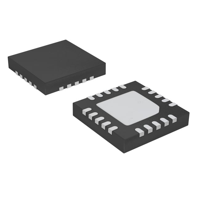
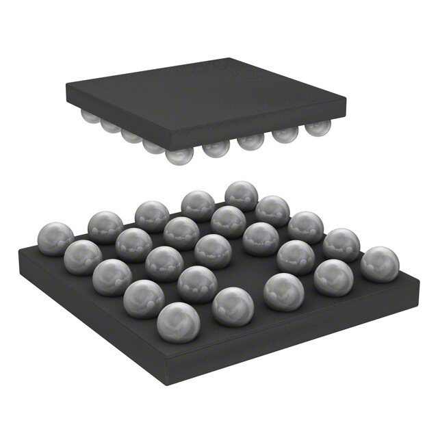
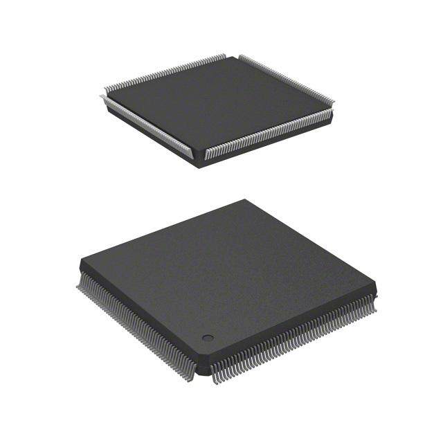
| 描述 | IC TRANSP LATCH OCT D 20DHVQFN |
| 产品分类 | |
| 品牌 | NXP Semiconductors |
| 数据手册 | |
| 产品图片 |
|
| 产品型号 | 74AHCT573BQ,115 |
| PCN封装 | |
| PCN组件/产地 | |
| rohs | 无铅 / 符合限制有害物质指令(RoHS)规范要求 |
| 产品系列 | 74AHCT |
| 供应商器件封装 | 20-DHVQFN(4.5x 2.5) |
| 其它名称 | 568-5384-6 |
| 包装 | Digi-Reel® |
| 安装类型 | 表面贴装 |
| 封装/外壳 | 20-VFQFN 裸露焊盘 |
| 工作温度 | -40°C ~ 125°C |
| 延迟时间-传播 | 3.5ns |
| 标准包装 | 1 |
| 独立电路 | 1 |
| 电压-电源 | 4.5 V ~ 5.5 V |
| 电流-输出高,低 | 8mA,8mA |
| 电路 | 8:8 |
| 输出类型 | 三态 |
| 逻辑类型 | D 型透明锁存器 |


- 商务部:美国ITC正式对集成电路等产品启动337调查
- 曝三星4nm工艺存在良率问题 高通将骁龙8 Gen1或转产台积电
- 太阳诱电将投资9.5亿元在常州建新厂生产MLCC 预计2023年完工
- 英特尔发布欧洲新工厂建设计划 深化IDM 2.0 战略
- 台积电先进制程称霸业界 有大客户加持明年业绩稳了
- 达到5530亿美元!SIA预计今年全球半导体销售额将创下新高
- 英特尔拟将自动驾驶子公司Mobileye上市 估值或超500亿美元
- 三星加码芯片和SET,合并消费电子和移动部门,撤换高东真等 CEO
- 三星电子宣布重大人事变动 还合并消费电子和移动部门
- 海关总署:前11个月进口集成电路产品价值2.52万亿元 增长14.8%


PDF Datasheet 数据手册内容提取
74AHC573; 74AHCT573 Octal D-type transparant latch; 3-state Rev. 7 — 8 November 2011 Product data sheet 1. General description The 74AHC573; 74AHCT573 is a high-speed Si-gate CMOS device and is pin compatible with Low-power Schottky TTL (LSTTL). It is specified in compliance with JEDEC standard No.7A. The 74AHC573; 74AHCT573 consists of eight D-type transparent latches featuring separate D-type inputs for each latch and 3-state true outputs for bus oriented applications. A latch enable input (LE) and an output enable input (OE) are common to all latches. When pinLE is HIGH, data at the Dn inputs enters the latches. In this condition the latches are transparent, i.e. a latch output will change state each time its corresponding Dn input changes. When pin LE is LOW, the latches store the information that is present at the Dn inputs, after a set-up time preceding the HIGH-to-LOW transition of LE. When pinOE is LOW, the contents of the 8latches are available at the outputs. When pinOE is HIGH, the outputs go to the high-impedance OFF-state. Operation of the OE input does not affect the state of the latches. The 74AHC573; 74AHCT573 is functionally identical to the 74AHC373; 74AHCT373, but has a different pin arrangement. 2. Features and benefits Balanced propagation delays All inputs have a Schmitt trigger action Common 3-state output enable input Functionally identical to the 74AHC373; 74AHCT373 Inputs accept voltages higher than V CC Input levels: For 74AHC573: CMOS input level For 74AHCT573: TTL input level ESD protection: HBM EIA/JESD22-A114E exceeds 2000V MM EIA/JESD22-A115-A exceeds 200V CDM EIA/JESD22-C101C exceeds 1000V Multiple package options Specified from 40C to +85C and from 40C to +125C
74AHC573; 74AHCT573 Nexperia Octal D-type transparant latch; 3-state 3. Ordering information Table 1. Ordering info rmation Type number Package Temperature range Name Description Version 74AHC573 74AHC573D 40Cto+125C SO20 plastic small outline package; 20leads; SOT163-1 bodywidth7.5mm 74AHC573PW 40Cto+125C TSSOP20 plastic thin shrink small outline package; 20leads; SOT360-1 bodywidth4.4mm 74AHC573BQ 40Cto+125C DHVQFN20 plastic dual in-line compatible thermal enhanced SOT764-1 very thin quad flat package noleads; 20 terminals; body 2.54.50.85mm 74AHCT573 74AHCT573D 40Cto+125C SO20 plastic small outline package; 20leads; SOT163-1 bodywidth7.5mm 74AHCT573PW 40Cto+125C TSSOP20 plastic thin shrink small outline package; 20leads; SOT360-1 bodywidth4.4mm 74AHCT573BQ 40Cto+125C DHVQFN20 plastic dual in-line compatible thermal enhanced SOT764-1 very thin quad flat package noleads; 20 terminals; body 2.54.50.85mm 4. Functional diagram 2 D0 Q0 19 3 D1 Q1 18 4 D2 Q2 17 5 D3 Q3 16 LATCH 3-STATE 6 D4 1 to 8 OUTPUTS Q4 15 7 D5 Q5 14 8 D6 Q6 13 9 D7 Q7 12 11 LE 1 OE mna809 Fig 1. Functional diagram 74AHC_AHCT573 All information provided in this document is subject to legal disclaimers. © Nexperia B.V. 2017. All rights reserved Product data sheet Rev. 7 — 8 November 2011 2 of 19
74AHC573; 74AHCT573 Nexperia Octal D-type transparant latch; 3-state 11 C1 1 EN1 1 2 19 OE 1D 2 19 D0 Q0 3 18 3 18 D1 Q1 4 17 4 17 D2 Q2 5 16 5 16 D3 Q3 6 15 6 15 D4 Q4 7 14 D5 Q5 7 14 8 13 D6 Q6 8 13 9 12 D7 Q7 9 12 LE 11 mna807 mna808 Fig 2. Logic symbol Fig 3. IEC logic symbol D0 D1 D2 D3 D4 D5 D6 D7 D Q D Q D Q D Q D Q D Q D Q D Q LATCH LATCH LATCH LATCH LATCH LATCH LATCH LATCH 1 2 3 4 5 6 7 8 LE LE LE LE LE LE LE LE LE LE LE LE LE LE LE LE LE OE Q0 Q1 Q2 Q3 Q4 Q5 Q6 Q7 mna810 Fig 4. Logic diagram 74AHC_AHCT573 All information provided in this document is subject to legal disclaimers. © Nexperia B.V. 2017. All rights reserved Product data sheet Rev. 7 — 8 November 2011 3 of 19
74AHC573; 74AHCT573 Nexperia Octal D-type transparant latch; 3-state 5. Pinning information 5.1 Pinning 74AHC573 74AHCT573 terminal 1 E CC index area O V 1 20 D0 2 19 Q0 D1 3 18 Q1 OE 1 20 VCC D2 4 17 Q2 D0 2 19 Q0 D3 5 16 Q3 D1 3 18 Q1 D2 4 17 Q2 D4 6 15 Q4 D3 5 16 Q3 D5 7 14 Q5 573 D4 6 15 Q4 D6 8 GND(1) 13 Q6 D5 7 14 Q5 D7 9 12 Q7 D6 8 13 Q6 0 1 1 1 D7 9 12 Q7 D E GND 10 11 LE GN L 001aal532 001aad099 Transparent top view (1) This is not a supply pin. The substrate is attached to this pad using conductive die attach material. There is no electrical or mechanical requirement to solder this pad. However, if it is soldered, the solder land should remain floating or be connected to GND. Fig 5. Pin configuration SO20 and TSSOP20 Fig 6. Pin configuration DHVQFN20 5.2 Pin description Table 2. Pin descripti on Symbol Pin Description OE 1 output enable input (active LOW) D0 to D7 2, 3, 4, 5, 6, 7, 8, 9 data input GND 10 ground (0V) LE 11 latch enable (active HIGH) Q0 to Q7 19, 18, 17, 16, 15, 14, 13, 12 data output V 20 supply voltage CC 74AHC_AHCT573 All information provided in this document is subject to legal disclaimers. © Nexperia B.V. 2017. All rights reserved Product data sheet Rev. 7 — 8 November 2011 4 of 19
74AHC573; 74AHCT573 Nexperia Octal D-type transparant latch; 3-state 6. Functional description Table 3. Function tab le[1] Operating mode Input Internal latch Output OE LE Dn Qn Enable and read register (transparent L H L L L mode) H H H Latch and read register L L l L L h H H Latch register and disable outputs H L l L Z h H Z [1] H=HIGH voltage level; h =HIGH voltage level one set-up time prior to the HIGH-to-LOW LE transition; L=LOW voltage level; l=LOW voltage level one set-up time prior to the HIGH-to-LOW LE transition; Z=high-impedance OFF-state. 7. Limiting values Table 4. Limiting valu es In accordance with the Absolute Maximum Rating System (IEC 60134).Voltages are referenced to GND (ground = 0V). Symbol Parameter Conditions Min Max Unit V supply voltage 0.5 +7.0 V CC V input voltage 0.5 +7.0 V I I input clamping current V < 0.5V [1] 20 - mA IK I I output clamping current V <0.5V orV >V +0.5V [1] 20 +20 mA OK O O CC I output current V = 0.5V to (V +0.5V) 25 +25 mA O O CC I supply current - +75 mA CC I ground current 75 - mA GND T storage temperature 65 +150 C stg P total power dissipation T = 40 C to +125C [2] - 500 mW tot amb [1] The input and output voltage ratings may be exceeded if the input and output current ratings are observed. [2] For SO20 packages: above 70C the value of Ptot derates linearly at 8mW/K. For TSSOP20 packages: above 60C the value of Ptot derates linearly at 5.5mW/K. For DHVQFN20 packages: above 60C the value of Ptot derates linearly with 4.5mW/K. 74AHC_AHCT573 All information provided in this document is subject to legal disclaimers. © Nexperia B.V. 2017. All rights reserved Product data sheet Rev. 7 — 8 November 2011 5 of 19
74AHC573; 74AHCT573 Nexperia Octal D-type transparant latch; 3-state 8. Recommended operating conditions Table 5. Operating co nditions Symbol Parameter Conditions Min Typ Max Unit 74AHC573 V supply voltage 2.0 5.0 5.5 V CC V input voltage 0 - 5.5 V I V output voltage 0 - V V O CC T ambient temperature 40 +25 +125 C amb t/V input transition rise and fall rate V = 3.0 V to 3.6 V - - 100 ns/V CC V = 4.5 V to 5.5 V - - 20 ns/V CC 74AHCT573 V supply voltage 4.5 5.0 5.5 V CC V input voltage 0 - 5.5 V I V output voltage 0 - V V O CC T ambient temperature 40 +25 +125 C amb t/V input transition rise and fall rate V = 4.5 V to 5.5 V - - 20 ns/V CC 9. Static characteristics Table 6. Static charac teristics At recommended operating conditions; voltages are referenced to GND (ground = 0V). Symbol Parameter Conditions 25 C 40C to+85 C 40C to+125 C Unit Min Typ Max Min Max Min Typ Max 74AHC573 V HIGH-level V = 2.0 V 1.5 - - 1.5 - 1.5 - - V IH CC input voltage V = 3.0 V 2.1 - - 2.1 - 2.1 - - V CC V = 5.5 V 3.85 - - 3.85 - 3.85 - - V CC V LOW-level V = 2.0 V - - 0.5 - 0.5 - - 0.5 V IL CC input voltage V = 3.0 V - - 0.9 - 0.9 - - 0.9 V CC V = 5.5 V - - 1.65 - 1.65 - - 1.65 V CC V HIGH-level V = V or V OH I IH IL output voltage I = 50A; V =2.0 V 1.9 2.0 - 1.9 - 1.9 - - V O CC I = 50A; V =3.0 V 2.9 3.0 - 2.9 - 2.9 - - V O CC I = 50A; V =4.5 V 4.4 4.5 - 4.4 - 4.4 - - V O CC I = 4.0mA; V =3.0 V 2.58 - - 2.48 - 2.40 - - V O CC I = 8.0mA; V =4.5 V 3.94 - - 3.80 - 3.70 - - V O CC V LOW-level V = V or V OL I IH IL output voltage I = 50A; V =2.0 V - 0 0.1 - 0.1 - - 0.1 V O CC I = 50A; V =3.0 V - 0 0.1 - 0.1 - - 0.1 V O CC I = 50A; V =4.5 V - 0 0.1 - 0.1 - - 0.1 V O CC I = 4.0mA; V =3.0 V - - 0.36 - 0.44 - - 0.55 V O CC I = 8.0mA; V =4.5 V - - 0.36 - 0.44 - - 0.55 V O CC 74AHC_AHCT573 All information provided in this document is subject to legal disclaimers. © Nexperia B.V. 2017. All rights reserved Product data sheet Rev. 7 — 8 November 2011 6 of 19
74AHC573; 74AHCT573 Nexperia Octal D-type transparant latch; 3-state Table 6. Static characteristics …continued At recommended operating conditions; voltages are referenced to GND (ground = 0V). Symbol Parameter Conditions 25 C 40C to+85 C 40C to+125 C Unit Min Typ Max Min Max Min Typ Max I OFF-state V =V orV ; - - 0.25 - 2.5 - - 10.0 A OZ I IH IL output current V =V orGND; O CC V =5.5V CC I input leakage V =V orGND; - - 0.1 - 1.0 - - 2.0 A I I CC current V =0Vto 5.5V CC I supply current V =V orGND;I =0A; - - 4.0 - 40 - - 80 A CC I CC O V =5.5V CC C input V =V orGND - 3 10 - 10 - - 10 pF I I CC capacitance C output - 4 - - - - - 10 pF O capacitance 74AHCT573 V HIGH-level V = 4.5 V to 5.5 V 2.0 - - 2.0 - 2.0 - - V IH CC input voltage V LOW-level V = 4.5 V to 5.5 V - - 0.8 - 0.8 - - 0.8 V IL CC input voltage V HIGH-level V = V or V ; V =4.5 V OH I IH IL CC output voltage I = 50A 4.4 4.5 - 4.4 - 4.4 - - V O I = 8.0mA 3.94 - - 3.80 - 3.70 - - V O V LOW-level V = V or V ; V =4.5 V OL I IH IL CC output voltage I = 50A - 0 0.1 - 0.1 - - 0.1 V O I = 8.0mA - - 0.36 - 0.44 - - 0.55 V O I OFF-state V =V orV ; - - 0.25 - 2.5 - - 10.0 A OZ I IH IL output current V =V orGND per input O CC pin; other inputs at V or CC GND; I =0 A O I input leakage V =5.5 VorGND; - - 0.1 - 1.0 - - 2.0 A I I current V =0Vto 5.5V CC I supply current V =V orGND; I = 0 A; - - 4.0 - 40 - - 80 A CC I CC O V =5.5V CC I additional per input pin; - - 1.35 - 1.5 - - 1.5 mA CC supply current V =V 2.1V; I =0 A; I CC O otherpinsatV or GND; CC V =4.5Vto5.5V CC C input V =V orGND - 3 10 - 10 - - 10 pF I I CC capacitance C output - 4 - - - - - 10 pF O capacitance 74AHC_AHCT573 All information provided in this document is subject to legal disclaimers. © Nexperia B.V. 2017. All rights reserved Product data sheet Rev. 7 — 8 November 2011 7 of 19
74AHC573; 74AHCT573 Nexperia Octal D-type transparant latch; 3-state 10. Dynamic characteristics Table 7. Dynamic cha racteristics Voltages are referenced to GND (ground = 0 V); for test circuit see Figure11. Symbol Parameter Conditions 25 C 40C to+85 C 40C to+125 C Unit Min Typ[1] Max Min Max Min Max 74AHC573 t propagation DntoQn; see Figure7 [2] pd delay V = 3.0 V to 3.6 V CC C =15pF - 5.5 11.0 1.0 13.0 1.0 14.0 ns L C =50pF - 7.8 14.5 1.0 16.5 1.0 18.5 ns L V = 4.5 V to 5.5 V CC C =15pF - 3.9 6.8 1.0 8.0 1.0 8.5 ns L C =50pF - 5.5 8.8 1.0 10.0 1.0 11.0 ns L LEtoQn; see Figure8 [2] V = 3.0 V to 3.6 V CC C =15pF - 5.8 11.9 1.0 14.0 1.0 15.0 ns L C =50pF - 8.3 15.4 1.0 17.5 1.0 19.5 ns L V = 4.5 V to 5.5 V CC C =15pF - 4.2 7.7 1.0 9.0 1.0 10.0 ns L C =50pF - 5.9 9.7 1.0 11.0 1.0 12.5 ns L t enable time OEtoQn; see Figure9 [3] en V = 3.0 V to 3.6 V CC C =15pF - 5.8 11.5 1.0 13.5 1.0 14.5 ns L C =50pF - 8.3 15.0 1.0 17.0 1.0 19.0 ns L V = 4.5 V to 5.5 V CC C =15pF - 4.4 7.7 1.0 9.0 1.0 10.0 ns L C =50pF - 6.3 9.7 1.0 11.0 1.0 12.5 ns L t disable time OEtoQn; see Figure9 [4] dis V = 3.0 V to 3.6 V CC C =15pF - 6.8 11.0 1.0 13.0 1.0 14.0 ns L C =50pF - 9.7 14.5 1.0 16.5 1.0 18.5 ns L V = 4.5 V to 5.5 V CC C =15pF - 4.6 7.7 1.0 9.0 1.0 10.0 ns L C =50pF - 7.4 9.7 1.0 11.0 1.0 12.5 ns L t pulse width LE HIGH; seeFigure8 W V =3.0 V to 3.6 V 5.0 - - 5.0 - 5.0 - ns CC V =4.5 V to 5.5 V 5.0 - - 5.0 - 5.0 - ns CC t set-up time DntoLE; see Figure10 su V =3.0 V to 3.6 V 3.5 - - 3.5 - 3.5 - ns CC V =4.5 V to 5.5 V 3.5 - - 3.5 - 3.5 - ns CC 74AHC_AHCT573 All information provided in this document is subject to legal disclaimers. © Nexperia B.V. 2017. All rights reserved Product data sheet Rev. 7 — 8 November 2011 8 of 19
74AHC573; 74AHCT573 Nexperia Octal D-type transparant latch; 3-state Table 7. Dynamic characteristics …continued Voltages are referenced to GND (ground = 0 V); for test circuit see Figure11. Symbol Parameter Conditions 25 C 40C to+85 C 40C to+125 C Unit Min Typ[1] Max Min Max Min Max t hold time Dn to LE; see Figure10 h V =3.0 V to 3.6 V 1.5 - - 1.5 - 1.5 - ns CC V =4.5 V to 5.5 V 1.5 - - 1.5 - 1.5 - ns CC C power f = 1 MHz; [5] - 12 - - - - - pF PD i dissipation V =GNDtoV I CC capacitance 74AHCT573; V = 4.5 V to 5.5 V CC t propagation DntoQn; see Figure7 [2] pd delay C =15pF - 3.5 5.5 1 6.5 1 7.0 ns L C =50pF - 4.9 7.5 1 8.5 1 9.5 ns L LEtoQn; see Figure8 [2] C =15pF - 3.9 6.0 1 7.0 1 7.5 ns L C =50pF - 5.5 8.5 1 9.5 1 11.0 ns L t enable time OEtoQn; see Figure9 [3] en C =15pF - 4.1 6.5 1 7.5 1 8.5 ns L C =50pF - 5.9 8.5 1 10.0 1 11.0 ns L t disable time OEtoQn; see Figure9 [4] dis C =15pF - 4.5 6.5 1 7.5 1 8.5 ns L C =50pF - 6.4 9.0 1 10.0 1 11.5 ns L t pulse width LE HIGH; seeFigure8 5.0 - - 5.0 - 5.0 - ns W t set-up time DntoLE; see Figure10 3.5 - - 3.5 - 3.5 - ns su t hold time Dn to LE; see Figure10 1.5 - - 1.5 - 1.5 - ns h C power f = 1 MHz; [5] - 18 - - - - - pF PD i dissipation V =GNDtoV I CC capacitance [1] Typical values are measured at nominal supply voltage (V = 3.3V and V = 5.0V). CC CC [2] t is the same as t and t . pd PHL PLH [3] t is the same as t and t . en PZH PZL [4] t is the same as t and t . dis PHZ PLZ [5] CPD is used to determine the dynamic power dissipation (PD in W). PD=CPDVCC2fiN+(CLVCC2fo)where: f = input frequency in MHz; i f =output frequency in MHz; o C =output load capacitance inpF; L V =supply voltage in V; CC N=number of inputs switching; (CLVCC2fo)=sum of the outputs. 74AHC_AHCT573 All information provided in this document is subject to legal disclaimers. © Nexperia B.V. 2017. All rights reserved Product data sheet Rev. 7 — 8 November 2011 9 of 19
74AHC573; 74AHCT573 Nexperia Octal D-type transparant latch; 3-state 11. Waveforms VI Dn input VM GND tPHL tPLH VOH Qn output VM VOL mna811 Measurement points are given in Table8. VOL and VOH are typical voltage output levels that occur with the output load. Fig 7. Data input to output propagation delays 1/fmax VI LE input VM GND tW tPHL tPLH VOH Qn output VM VOL mna812 V and V are typical voltage output levels that occur with the output load. OL OH Fig 8. Latch enable input to output propagation delays 74AHC_AHCT573 All information provided in this document is subject to legal disclaimers. © Nexperia B.V. 2017. All rights reserved Product data sheet Rev. 7 — 8 November 2011 10 of 19
74AHC573; 74AHCT573 Nexperia Octal D-type transparant latch; 3-state VI OE input VM GND tPLZ tPZL VCC Qn output LOW-to-OFF VM OFF-to-LOW VOL VX tPHZ tPZH Qn output VOH VY HIGH-to-OFF VM OFF-to-HIGH GND outputs outputs outputs enabled disabled enabled mna813 Measurement points are given in Table8. VOL and VOH are typical voltage output levels that occur with the output load. Fig 9. Enable and disable times VI Dn input VM GND th th tsu tsu VI LE input VM GND mna814 Measurement points are given in Table8. V and V are typical voltage output levels that occur with the output load. OL OH The shaded areas indicate when the input is permitted to change for predicable output performance. Fig 10. Data set-up and hold times Table 8. Measuremen t points Type Input Output V V V V M M X Y 74AHC573 0.5V 0.5V V + 0.3 V V 0.3 V CC CC OL OH 74AHCT573 1.5 V 0.5V V + 0.3 V V 0.3 V CC OL OH 74AHC_AHCT573 All information provided in this document is subject to legal disclaimers. © Nexperia B.V. 2017. All rights reserved Product data sheet Rev. 7 — 8 November 2011 11 of 19
74AHC573; 74AHCT573 Nexperia Octal D-type transparant latch; 3-state tW VI 90 % negative pulse VM VM 10 % 0 V tf tr tr tf VI 90 % positive pulse VM VM 10 % 0 V tW VCC VCC VI VO RL S1 G DUT open RT CL 001aad983 Test data is given in Table9. Definitions test circuit: RT = termination resistance should be equal to output impedance Zo of the pulse generator. CL = load capacitance including jig and probe capacitance. R = load resistance. L S1 = test selection switch. Fig 11. Test circuitry for switching times Table 9. Test data Type Input Load S1 position V t, t C R t , t t , t t , t I r f L L PHL PLH PZH PHZ PZL PLZ 74AHC573 V 3.0ns 15pF, 50pF 1k open GND V CC CC 74AHCT573 3.0V 3.0ns 15pF, 50pF 1k open GND V CC 74AHC_AHCT573 All information provided in this document is subject to legal disclaimers. © Nexperia B.V. 2017. All rights reserved Product data sheet Rev. 7 — 8 November 2011 12 of 19
74AHC573; 74AHCT573 Nexperia Octal D-type transparant latch; 3-state 12. Package outline SO20: plastic small outline package; 20 leads; body width 7.5 mm SOT163-1 D E A X c y HE v M A Z 20 11 Q A2 A A1 (A 3 ) pin 1 index θ Lp L 1 10 detail X e w M bp 0 5 10 mm scale DIMENSIONS (inch dimensions are derived from the original mm dimensions) UNIT mAax. A1 A2 A3 bp c D(1) E(1) e HE L Lp Q v w y Z(1) θ 0.3 2.45 0.49 0.32 13.0 7.6 10.65 1.1 1.1 0.9 mm 2.65 0.25 1.27 1.4 0.25 0.25 0.1 0.1 2.25 0.36 0.23 12.6 7.4 10.00 0.4 1.0 0.4 8o 0.012 0.096 0.019 0.013 0.51 0.30 0.419 0.043 0.043 0.035 0o inches 0.1 0.01 0.05 0.055 0.01 0.01 0.004 0.004 0.089 0.014 0.009 0.49 0.29 0.394 0.016 0.039 0.016 Note 1. Plastic or metal protrusions of 0.15 mm (0.006 inch) maximum per side are not included. OUTLINE REFERENCES EUROPEAN ISSUE DATE VERSION IEC JEDEC JEITA PROJECTION 99-12-27 SOT163-1 075E04 MS-013 03-02-19 Fig 12. Package outline SOT163-1 (SO20) 74AHC_AHCT573 All information provided in this document is subject to legal disclaimers. © Nexperia B.V. 2017. All rights reserved Product data sheet Rev. 7 — 8 November 2011 13 of 19
74AHC573; 74AHCT573 Nexperia Octal D-type transparant latch; 3-state TSSOP20: plastic thin shrink small outline package; 20 leads; body width 4.4 mm SOT360-1 D E A X c y HE v M A Z 20 11 Q A2 (A 3 ) A pin 1 index A1 θ Lp L 1 10 detail X w M e bp 0 2.5 5 mm scale DIMENSIONS (mm are the original dimensions) UNIT mAax. A1 A2 A3 bp c D(1) E(2) e HE L Lp Q v w y Z(1) θ mm 1.1 00..1055 00..9850 0.25 00..3109 00..21 66..64 44..53 0.65 66..62 1 00..7550 00..43 0.2 0.13 0.1 00..52 80oo Notes 1. Plastic or metal protrusions of 0.15 mm maximum per side are not included. 2. Plastic interlead protrusions of 0.25 mm maximum per side are not included. OUTLINE REFERENCES EUROPEAN ISSUE DATE VERSION IEC JEDEC JEITA PROJECTION 99-12-27 SOT360-1 MO-153 03-02-19 Fig 13. Package outline SOT360-1 (TSSOP20) 74AHC_AHCT573 All information provided in this document is subject to legal disclaimers. © Nexperia B.V. 2017. All rights reserved Product data sheet Rev. 7 — 8 November 2011 14 of 19
74AHC573; 74AHCT573 Nexperia Octal D-type transparant latch; 3-state DHVQFN20: plastic dual in-line compatible thermal enhanced very thin quad flat package; no leads; 20 terminals; body 2.5 x 4.5 x 0.85 mm SOT764-1 D B A A A1 E c terminal 1 detail X index area terminal 1 e1 C index area e b v M C A B y1 C y w M C 2 9 L 1 10 Eh e 20 11 19 12 Dh X 0 2.5 5 mm scale DIMENSIONS (mm are the original dimensions) A(1) UNIT max. A1 b c D(1) Dh E(1) Eh e e1 L v w y y1 0.05 0.30 4.6 3.15 2.6 1.15 0.5 mm 1 0.2 0.5 3.5 0.1 0.05 0.05 0.1 0.00 0.18 4.4 2.85 2.4 0.85 0.3 Note 1. Plastic or metal protrusions of 0.075 mm maximum per side are not included. OUTLINE REFERENCES EUROPEAN ISSUE DATE VERSION IEC JEDEC JEITA PROJECTION 02-10-17 SOT764-1 - - - MO-241 - - - 03-01-27 Fig 14. Package outline SOT764-1 (DHVQFN20) 74AHC_AHCT573 All information provided in this document is subject to legal disclaimers. © Nexperia B.V. 2017. All rights reserved Product data sheet Rev. 7 — 8 November 2011 15 of 19
74AHC573; 74AHCT573 Nexperia Octal D-type transparant latch; 3-state 13. Abbreviations Table 10. Abbreviations Acronym Description CDM Charged Device Model CMOS Complementary Metal-Oxide Semiconductor ESD ElectroStatic Discharge HBM Human Body Model MM Machine Model TTL Transistor-Transistor Logic 14. Revision history T able 11. Revision history Document ID Release date Data sheet status Change notice Supersedes 74AHC_AHCT573 v.7 20111108 Product data sheet - 74AHC_AHCT573 v.6 Modifications: • Legal pages updated. 74AHC_AHCT573 v.6 20101125 Product data sheet - 74AHC_AHCT573 v.5 74AHC_AHCT573 v.5 20100325 Product data sheet - 74AHC_AHCT573 v.4 74AHC_AHCT573 v.4 20100303 Product data sheet - 74AHC_AHCT573 v.3 74AHC_AHCT573 v.3 20080424 Product data sheet - 74AHC_AHCT573 v.2 74AHC_AHCT573 v.2 20031208 Product specification - 74AHC_AHCT573 v.1 74AHC_AHCT573 v.1 19990927 Product specification - - 74AHC_AHCT573 All information provided in this document is subject to legal disclaimers. © Nexperia B.V. 2017. All rights reserved Product data sheet Rev. 7 — 8 November 2011 16 of 19
74AHC573; 74AHCT573 Nexperia Octal D-type transparant latch; 3-state 15. Legal information 15.1 Data sheet status Document status[1][2] Product status[3] Definition Objective [short] data sheet Development This document contains data from the objective specification for product development. Preliminary [short] data sheet Qualification This document contains data from the preliminary specification. Product [short] data sheet Production This document contains the product specification. [1] Please consult the most recently issued document before initiating or completing a design. [2] The term ‘short data sheet’ is explained in section “Definitions”. [3] The product status of device(s) described in this document may have changed since this document was published and may differ in case of multiple devices. The latest product status information is available on the Internet at URLhttp://www.nexperia.com. 15.2 Definitions malfunction of a Nexperia product can reasonably be expected to result in personal injury, death or severe property or environmental damage. Nexperia accepts no liability for inclusion and/or use of Draft — The document is a draft version only. The content is still under Nexperia products in such equipment or applications and internal review and subject to formal approval, which may result in therefore such inclusion and/or use is at the customer’s own risk. modifications or additions. Nexperia does not give any representations or warranties as to the accuracy or completeness of Applications — Applications that are described herein for any of these information included herein and shall have no liability for the consequences of products are for illustrative purposes only. Nexperia makes no use of such information. representation or warranty that such applications will be suitable for the specified use without further testing or modification. Short data sheet — A short data sheet is an extract from a full data sheet with the same product type number(s) and title. A short data sheet is intended Customers are responsible for the design and operation of their applications for quick reference only and should not be relied upon to contain detailed and and products using Nexperia products, and Nexperia full information. For detailed and full information see the relevant full data accepts no liability for any assistance with applications or customer product sheet, which is available on request via the local Nexperia sales design. It is customer’s sole responsibility to determine whether the Nexperia office. In case of any inconsistency or conflict with the short data sheet, the product is suitable and fit for the customer’s applications and full data sheet shall prevail. products planned, as well as for the planned application and use of customer’s third party customer(s). Customers should provide appropriate Product specification — The information and data provided in a Product design and operating safeguards to minimize the risks associated with their data sheet shall define the specification of the product as agreed between applications and products. Nexperia and its customer, unless Nexperia and Nexperia does not accept any liability related to any default, customer have explicitly agreed otherwise in writing. In no event however, damage, costs or problem which is based on any weakness or default in the shall an agreement be valid in which the Nexperia product is customer’s applications or products, or the application or use by customer’s deemed to offer functions and qualities beyond those described in the third party customer(s). Customer is responsible for doing all necessary Product data sheet. testing for the customer’s applications and products using Nexperia products in order to avoid a default of the applications and 15.3 Disclaimers the products or of the application or use by customer’s third party customer(s). Nexperia does not accept any liability in this respect. Limited warranty and liability — Information in this document is believed to Limiting values — Stress above one or more limiting values (as defined in be accurate and reliable. However, Nexperia does not give any the Absolute Maximum Ratings System of IEC60134) will cause permanent representations or warranties, expressed or implied, as to the accuracy or damage to the device. Limiting values are stress ratings only and (proper) completeness of such information and shall have no liability for the operation of the device at these or any other conditions above those given in consequences of use of such information. the Recommended operating conditions section (if present) or the Characteristics sections of this document is not warranted. Constant or In no event shall Nexperia be liable for any indirect, incidental, repeated exposure to limiting values will permanently and irreversibly affect punitive, special or consequential damages (including - without limitation - lost the quality and reliability of the device. profits, lost savings, business interruption, costs related to the removal or replacement of any products or rework charges) whether or not such Terms and conditions of commercial sale — Nexperia damages are based on tort (including negligence), warranty, breach of products are sold subject to the general terms and conditions of commercial contract or any other legal theory. sale, as published at http://www.nexperia.com/profile/terms, unless otherwise Notwithstanding any damages that customer might incur for any reason agreed in a valid written individual agreement. In case an individual whatsoever, Nexperia’s aggregate and cumulative liability towards agreement is concluded only the terms and conditions of the respective customer for the products described herein shall be limited in accordance agreement shall apply. Nexperia hereby expressly objects to with the Terms and conditions of commercial sale of Nexperia. applying the customer’s general terms and conditions with regard to the purchase of Nexperia products by customer. Right to make changes — Nexperia reserves the right to make changes to information published in this document, including without No offer to sell or license — Nothing in this document may be interpreted or limitation specifications and product descriptions, at any time and without construed as an offer to sell products that is open for acceptance or the grant, notice. This document supersedes and replaces all information supplied prior conveyance or implication of any license under any copyrights, patents or to the publication hereof. other industrial or intellectual property rights. Suitability for use — Nexperia products are not designed, Export control — This document as well as the item(s) described herein authorized or warranted to be suitable for use in life support, life-critical or may be subject to export control regulations. Export might require a prior safety-critical systems or equipment, nor in applications where failure or authorization from competent authorities. 74AHC_AHCT573 All information provided in this document is subject to legal disclaimers. © Nexperia B.V. 2017. All rights reserved Product data sheet Rev. 7 — 8 November 2011 17 of 19
74AHC573; 74AHCT573 Nexperia Octal D-type transparant latch; 3-state Non-automotive qualified products — Unless this data sheet expressly Nexperia’s specifications such use shall be solely at customer’s states that this specific Nexperia product is automotive qualified, own risk, and (c) customer fully indemnifies Nexperia for any the product is not suitable for automotive use. It is neither qualified nor tested liability, damages or failed product claims resulting from customer design and in accordance with automotive testing or application requirements. Nexperia use of the product for automotive applications beyond Nexperia’s accepts no liability for inclusion and/or use of standard warranty and Nexperia’s product specifications. non-automotive qualified products in automotive equipment or applications. In the event that customer uses the product for design-in and use in 15.4 Trademarks automotive applications to automotive specifications and standards, customer (a) shall use the product without Nexperia’s warranty of the Notice: All referenced brands, product names, service names and trademarks product for such automotive applications, use and specifications, and (b) are the property of their respective owners. whenever customer uses the product for automotive applications beyond 16. Contact information For more information, please visit: http://www.nexperia.com For sales office addresses, please send an email to: salesaddresses@nexperia.com 74AHC_AHCT573 All information provided in this document is subject to legal disclaimers. © Nexperia B.V. 2017. All rights reserved Product data sheet Rev. 7 — 8 November 2011 18 of 19
74AHC573; 74AHCT573 Nexperia Octal D-type transparant latch; 3-state 17. Contents 1 General description. . . . . . . . . . . . . . . . . . . . . . 1 2 Features and benefits . . . . . . . . . . . . . . . . . . . . 1 3 Ordering information. . . . . . . . . . . . . . . . . . . . . 2 4 Functional diagram . . . . . . . . . . . . . . . . . . . . . . 2 5 Pinning information. . . . . . . . . . . . . . . . . . . . . . 4 5.1 Pinning . . . . . . . . . . . . . . . . . . . . . . . . . . . . . . . 4 5.2 Pin description . . . . . . . . . . . . . . . . . . . . . . . . . 4 6 Functional description . . . . . . . . . . . . . . . . . . . 5 7 Limiting values. . . . . . . . . . . . . . . . . . . . . . . . . . 5 8 Recommended operating conditions. . . . . . . . 6 9 Static characteristics. . . . . . . . . . . . . . . . . . . . . 6 10 Dynamic characteristics. . . . . . . . . . . . . . . . . . 8 11 Waveforms . . . . . . . . . . . . . . . . . . . . . . . . . . . . 10 12 Package outline. . . . . . . . . . . . . . . . . . . . . . . . 13 13 Abbreviations. . . . . . . . . . . . . . . . . . . . . . . . . . 16 14 Revision history. . . . . . . . . . . . . . . . . . . . . . . . 16 15 Legal information. . . . . . . . . . . . . . . . . . . . . . . 17 15.1 Data sheet status . . . . . . . . . . . . . . . . . . . . . . 17 15.2 Definitions. . . . . . . . . . . . . . . . . . . . . . . . . . . . 17 15.3 Disclaimers. . . . . . . . . . . . . . . . . . . . . . . . . . . 17 15.4 Trademarks. . . . . . . . . . . . . . . . . . . . . . . . . . . 18 16 Contact information. . . . . . . . . . . . . . . . . . . . . 18 17 Contents. . . . . . . . . . . . . . . . . . . . . . . . . . . . . . 19 © Nexperia B.V. 2017. All rights reserved For more information, please visit: http://www.nexperia.com For sales office addresses, please send an email to: salesaddresses@nexperia.com Date of release: 08 November 2011