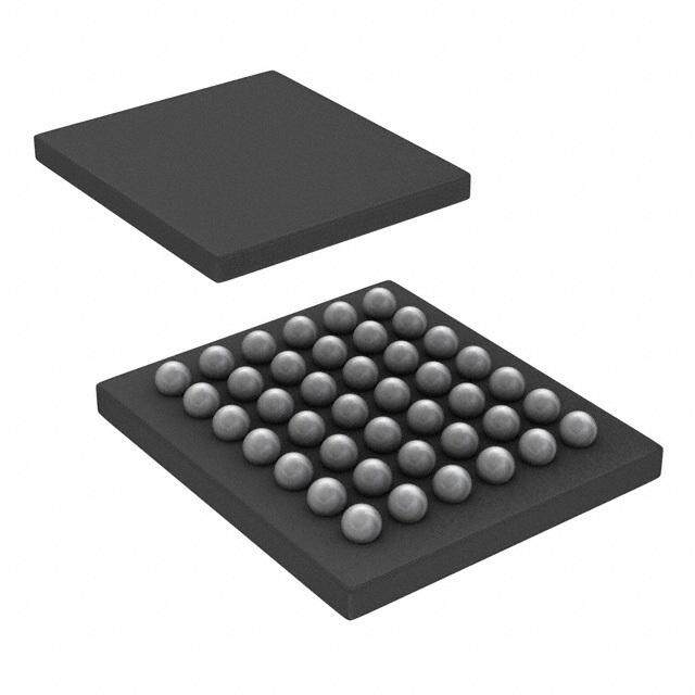
ICGOO在线商城 > 集成电路(IC) > PMIC - 电源管理 - 专用 > 73S8009R-IM/F
- 型号: 73S8009R-IM/F
- 制造商: Maxim
- 库位|库存: xxxx|xxxx
- 要求:
| 数量阶梯 | 香港交货 | 国内含税 |
| +xxxx | $xxxx | ¥xxxx |
查看当月历史价格
查看今年历史价格
73S8009R-IM/F产品简介:
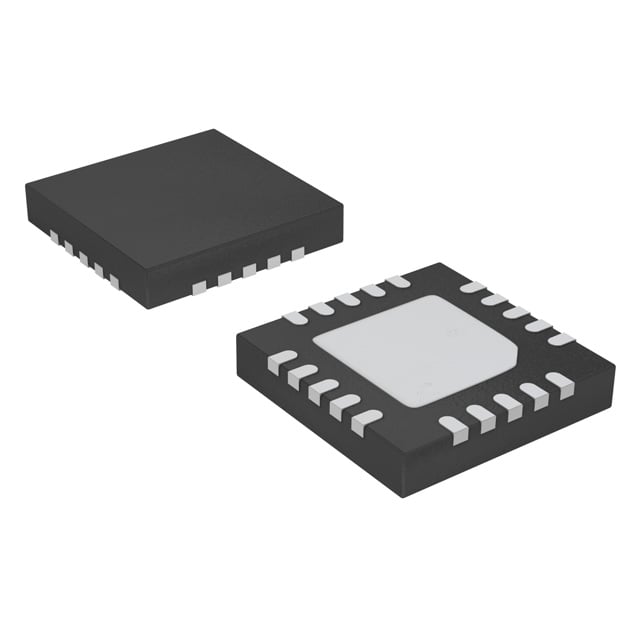
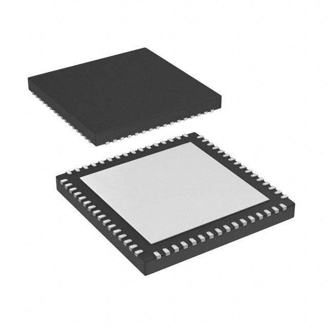
ICGOO电子元器件商城为您提供73S8009R-IM/F由Maxim设计生产,在icgoo商城现货销售,并且可以通过原厂、代理商等渠道进行代购。 73S8009R-IM/F价格参考。Maxim73S8009R-IM/F封装/规格:PMIC - 电源管理 - 专用, Smart Card Reader, Writer PMIC 20-QFN (4x4)。您可以下载73S8009R-IM/F参考资料、Datasheet数据手册功能说明书,资料中有73S8009R-IM/F 详细功能的应用电路图电压和使用方法及教程。
| 参数 | 数值 |
| 产品目录 | 集成电路 (IC)半导体 |
| 描述 | IC SMART CARD LEVEL SHIFT 20-QFN输入/输出控制器接口集成电路 Smart Card Interface IC |
| DevelopmentKit | 73S8009R-DB |
| 产品分类 | |
| 品牌 | Maxim Integrated |
| 产品手册 | |
| 产品图片 |
|
| rohs | 符合RoHS无铅 / 符合限制有害物质指令(RoHS)规范要求 |
| 产品系列 | 接口 IC,输入/输出控制器接口集成电路,Maxim Integrated 73S8009R-IM/F- |
| 数据手册 | |
| 产品型号 | 73S8009R-IM/F |
| 产品 | Smart Card Interface |
| 产品培训模块 | http://www.digikey.cn/PTM/IndividualPTM.page?site=cn&lang=zhs&ptm=25703http://www.digikey.cn/PTM/IndividualPTM.page?site=cn&lang=zhs&ptm=25705 |
| 产品种类 | 输入/输出控制器接口集成电路 |
| 供应商器件封装 | 20-QFN(4x4) |
| 其它名称 | 73S8009RIMF |
| 包装 | 托盘 |
| 商标 | Maxim Integrated |
| 安装类型 | 表面贴装 |
| 安装风格 | SMD/SMT |
| 封装 | Tube |
| 封装/外壳 | 20-VFQFN 裸露焊盘 |
| 封装/箱体 | QFN-20 |
| 工作温度 | -40°C ~ 85°C |
| 工作温度范围 | - 40 C to + 85 C |
| 工作电源电压 | 2.7 V to 6 V |
| 工厂包装数量 | 490 |
| 应用 | 智能卡读取器,写入器 |
| 应用说明 | |
| 最大工作温度 | + 85 C |
| 最小工作温度 | - 40 C |
| 标准包装 | 1 |
| 电压-电源 | 2.7 V ~ 3.6 V |
| 电流-电源 | - |
| 电源电流 | 700 uA |
| 系列 | 73S8009R |
| 零件号别名 | 73S8009R 90-W1009+XR3 |




PDF Datasheet 数据手册内容提取
73S8009R Low Cost Versatile Smart Card Interface Simplifying System Integration™ DATA SHEET DS_8009R_056 October 2009 APPLICATIONS • Set-Top-Box Conditional Access and Pay-per-View DESCRIPTION • SIM card readers in DECT and GSM phones, The 73S8009R is a very low-cost level shifter, single GPRS, WIFI and VOIP devices smart card (ICC) interface IC. The device includes a • Point of Sales & Transaction Terminals level shifter interface between a 3.3 V (typical) logic • General purpose smart card readers circuitry (host microcontroller) and an ISO-7816 / EMV smart card. The 73S8009R is designed to ADVANTAGES provide full electrical compliance with ISO-7816-3 EMV4.1 (EMV2000) and GSM11-11 specifications. • Lowest cost smart card interface IC on the market In normal operating mode, for maximum designer Ideal to replace discrete designs in POS flexibility, the host microcontroller is responsible for terminals and Set-Top-Boxes card activation and deactivation. The 73S8009R • Traditional step-up converter is replaced by incorporates an ISO-7816-3 deactivation sequencer an LDO regulator that controls the card signals in case of fault detection and card removal. Card presence and faults are Greatly reduced power dissipation reported to the host through an interrupt output. Fewer external components are required When the 73S8009R is ready to support a card with Better noise performance the selected voltage, a RDY signal informs the host it Very low power dissipation can initiate the card activation sequence. • Small format (4x4x0.8 mm) QFN20 package The 73S8009R supports 5V, 3V and 1.8V cards. option Selection is done through 2 dedicated digital inputs. Level-shifters drive the card signals with the selected FEATURES card voltage coming from an internal Low Drop-Out • Card Interface: (LDO) voltage regulator. The LDO regulator is powered by a dedicated power supply input, VPC. • Complies with ISO-7816-3, EMV 4.0 and Digital circuitry is separately powered by a digital GSM 11-11 specifications power supply, VDD. • An LDO voltage regulator provides 1.8V / 3V / 5V to the card from an external power Emergency card deactivation is initiated upon card supply input extraction or any fault generated by the protection • Provides at least 90 mA to the card circuitry. The fault can be a card over-current, a VDD (digital power), a VPC (regulator power), a VCC • ISO-7816-3 card emergency deactivation (card power output) or an over-heating fault. sequencer • Protection includes 3 voltage supervisors A chip select digital input drives internal latches that that detect voltage drops on V (card), V CC DD allow the host controller to control multiple (digital) and V (regulator) power supplies PC 73S8009R ICs in parallel. A power down digital • Over-current detection, 150 mA max. input also allows the host microcontroller to place • 2 card detection inputs, 1 for each user the IC in a very low-power mode making the 73S8009R particularly suitable for low-power and polarity battery-powered applications. • Auxiliary I/O lines for C4 / C8 contact signals Auxiliary I/O lines are also available (SO28 package • Card CLK clock frequency up to 20 MHz only) and make the 73S8009R suitable for all kind of cards, including synchronous (memory) cards. Rev. 1.3 © 2009 Teridian Semiconductor Corporation 1
73S8009R Data Sheet DS_8009R_056 • System Controller Interface • Regulator Power Supply (V ): PC • Five signal images of the card signals • Class A-B-C readers: 5V, 3V and 1.8V (RSTIN, CLKIN, IOUC, AUX1UC, AUX2UC) cards: 4.75 V to 6.0 V • Two inputs select card voltage (CMDVCC%, • Digital Interface (V ): 2.7 V to 3.6 V DD CMDVCC#) • 6 kV ESD protection on the card interface • Two Interrupt outputs (OFF, RDY) inform the • SO28 or QFN20 package system controller of card presence / faults and the interface status • Chip select input (CS) • Power down input (PWRDN) FUNCTIONAL DIAGRAM VDD VPC [17] 28 [9] 15 VCC FAULT VPC FAULT VOLTAGE REFERENCE vref LDO bias currents REGULATOR 8 [2] 20 [12] GND CMDVCC5 9 [3] CMDVCC3 22 [14] VCC 4 [20] CONTROL OFF LOGIC RESET 21 [13] RST 12 [6] BUFFER RDY 13 [7] PWRDN 1 [18] CS CLOCK 19 [11] CLK BUFFER 10 [4] RSTIN 26 [16] PRES 11 [5] CLKIN 16 [10] PRES 1.5MHz OVER TEMP FAULT R-C TEMP OSC. 5 [1] 25 [15] IOUC I/O AUX1UC 6 SMART CARD I/O BUFFERS 24 AUX1 7 23 AUX2UC AUX2 27 GND Pin numbers reference the SO28 package [Pin numbers] reference the QFN20 Package Figure 1: 73S8009R Block Diagram Rev. 1.3 2
DS_8009R_056 73S8009R Data Sheet Table of Contents 1 Pinout ............................................................................................................................................. 5 2 Electrical Specifications ................................................................................................................ 8 2.1 Absolute Maximum Ratings ..................................................................................................... 8 2.2 Recommended Operating Conditions ...................................................................................... 8 2.3 Smart Card Interface Requirements ........................................................................................ 9 2.4 Digital Signals Characteristics ............................................................................................... 11 2.5 DC Characteristics ................................................................................................................ 11 2.6 Voltage / Temperature Fault Detection Circuits ...................................................................... 12 3 Applications Information ............................................................................................................. 13 3.1 Example 73S8009R Schematics ........................................................................................... 13 3.2 System Controller Interface ................................................................................................... 14 3.3 Power Supply and Voltage Supervision ................................................................................. 14 3.4 Card Power Supply ............................................................................................................... 14 3.5 Over-temperature Monitor ..................................................................................................... 15 3.6 Activation and Deactivation Sequence................................................................................... 15 3.7 OFF and Fault Detection ....................................................................................................... 16 3.8 Power-down Operation.......................................................................................................... 17 3.9 Chip Select ........................................................................................................................... 18 3.10 I/O Circuitry and Timing......................................................................................................... 18 4 Mechanical Drawings .................................................................................................................. 20 4.1 20-pin QFN ........................................................................................................................... 20 4.2 28-Pin SO ............................................................................................................................. 21 5 Ordering Information ................................................................................................................... 22 6 Related Documentation ............................................................................................................... 22 7 Contact Information ..................................................................................................................... 22 Revision History .................................................................................................................................. 23 Rev. 1.3 3
73S8009R Data Sheet DS_8009R_056 Figures Figure 1: 73S8009R Block Diagram ......................................................................................................... 2 Figure 2: 73S8009R 20-Pin QFN Pinout .................................................................................................. 5 Figure 3: 73S8009R 28-Pin SO Pinout ..................................................................................................... 5 Figure 4: Typical 73S8009R Application Schematic ............................................................................... 13 Figure 5: Activation Sequence ............................................................................................................... 15 Figure 6: Deactivation Sequence ........................................................................................................... 16 Figure 7: OFF Activity Outside and Inside a Card Session ..................................................................... 17 Figure 8: Power-down Operation ........................................................................................................... 17 Figure 9: CS Timing Definitions.............................................................................................................. 18 Figure 10: I/O and I/OUC State Diagram ................................................................................................ 19 Figure 11: I/O to I/OUC Delay Timing Diagram....................................................................................... 19 Figure 12: 20-pin QFN Package Dimensions ......................................................................................... 20 Figure 13: 28-Pin SO Package Dimensions ........................................................................................... 21 Tables Table 1: 73S8009R Pin Definitions .......................................................................................................... 6 Table 2: Absolute Maximum Device Ratings ............................................................................................ 8 Table 3: Recommended Operating Conditions ......................................................................................... 8 Table 4: DC Smart Card Interface Requirements ..................................................................................... 9 Table 5: Digital Signals Characteristics .................................................................................................. 11 Table 6: DC Characteristics ................................................................................................................... 11 Table 7: Voltage / Temperature Fault Detection Circuits ......................................................................... 12 Table 8: Choice of VCC Pin Capacitor ................................................................................................... 15 Table 9: Order Numbers and Packaging Marks ...................................................................................... 22 4 Rev. 1.3
DS_8009R_056 73S8009R Data Sheet 1 Pinout The 73S8009R is supplied as a 20-pin QFN package and as a 28-pin SO package. 1 T S F S D E F E S D R O T C V P 0 9 8 7 6 2 1 1 1 1 I/OUC 1 15 I/O CMDVCC% 2 14 VCC TERIDIAN CMDVCC# 3 13 RST 73S8009R RSTIN 4 12 GND CLKIN 5 11 CLK 0 6 7 8 9 1 Y N 2 C D D T P S R R S V E W E R T P P Figure 2: 73S8009R 20-Pin QFN Pinout (Top View) CS 1 28 VDD TEST1 2 27 GND N/C 3 26 PRES OFF 4 25 I/O I/OUC 5 24 AUX1 AUX1UC 6 23 AUX2 AUX2UC 7 22 VCC CMDVCC% 8 21 RST CMDVCC# 9 20 GND RSTIN 10 19 CLK CLKIN 11 18 N/C RDY 12 17 N/C PWRDN 13 16 PRES TEST2 14 15 VPC Figure 3: 73S8009R 28-Pin SO Pinout Rev. 1.3 5
73S8009R Data Sheet DS_8009R_056 Table 1 describes the pin functions for the device. Table 1: 73S8009R Pin Definitions Pin Pin Pin Type Description Name (SO28) (QFN20) Card Interface I/O 25 15 IO Card I/O: Data signal to/from card. Includes a pull-up resistor to V CC. AUX1 24 NA IO AUX1: Auxiliary data signal to/from card. Includes a pull-up resistor to V CC. AUX2 23 NA IO AUX2: Auxiliary data signal to/from card. Includes a pull-up resistor to V CC. RST 21 13 O Card reset: provides reset signal to card. CLK 19 11 O Card clock: provides clock signal to card. The rate of this clock is determined by the external clock frequency provided on pin CLKIN. PRES 26 16 I Card Presence switch: active high indicates card is present. Should be tied to GND when not used, but includes a high- impedance pull-down current source. PRES 16 10 I Card Presence switch: active low indicates card is present. Should be tied to VDD when not used, but includes a high- impedance pull-up current source. VCC 22 14 PSO Card power supply – logically controlled by the sequencer, output of LDO regulator. Requires an external filter capacitor to GND. GND 20 NA GND Card ground. Miscellaneous Inputs and Outputs CLKIN 11 5 I Clock source for the card clock. TEST1 2 19 – This pin must be tied to GND in typical applications. TEST2 14 8 – This pin must be tied to GND in typical applications. NC 3,17,18 NA – Non-connected pin. Power Supply and Ground VDD 28 17 System interface supply voltage and supply voltage for internal circuitry. VPC 15 9 LDO regulator power supply source. GND 27 12 GND Ground. Microcontroller Interface CS 1 18 I When CS = 1, the control and signal pins are configured normally. When CS is set low, CMDVCC%, RSTIN, and CMDVCC# are latched, IOUC, AUX1UC, and AUX2UC are set to high-impedance pull-up mode and do not pass data to or from the smart card. Signals RDY and OFF are disabled to prevent a low output and the internal pull-up resistors are disconnected. OFF 4 20 O Interrupt signal to the processor. Active low, multi-function indicating fault conditions and card presence. Open drain output configuration. It includes an internal 20 kΩ pull-up to VDD. The pull-up is disabled in PWRDN and CS=0 modes. 6 Rev. 1.3
DS_8009R_056 73S8009R Data Sheet Pin Pin Pin Type Description Name (SO28) (QFN20) I/OUC 5 1 I/O System controller data I/O to/from the card. Includes a pull- up resistor to V DD. AUX1UC 6 NA I/O System controller auxiliary data I/O to/from the card. Includes a pull-up resistor to V DD. AUX2UC 7 NA I/O System controller auxiliary data I/O to/from the card. Includes a pull-up resistor to V DD. CMDVCC% 8 2 I Logic low on one or both of these pins will cause the LDO to CMDVCC# 9 3 I ramp the Vcc supply to the smart card and smart card interface to the value described in the following table: CMDVCC% CMDVCC# V Output Voltage CC 0 0 1.8 V 0 1 5.0 V 1 0 3.0 V 1 1 LDO off Refer to for additional information on the CMDVCC% and CMDVCC# operation. RSTIN 10 4 I Reset Input. This signal is the reset command to the card. RDY 12 6 O Signal to controller indicating the 73S8009R is ready because V is above the required value after CMDVCC% CC and/or CMDVCC# is asserted low. A 20 KΩ pull-up resistor to V is provided internally. The pull-up is disabled in DD PWRDN and CS=0 modes. PWRDN 13 7 I PWRDN=1 puts the circuit into low-power mode with all analog functions disabled. The circuit will recover from the PWRDN state in the same manner as recovery from a POR event, taking approximately 1 ms. PWRDN assertion when either CMDVCC% or CMDVCC# is low has no effect and is ignored. There is no pull-up or pull-down provided on this pin. Rev. 1.3 7
73S8009R Data Sheet DS_8009R_056 2 Electrical Specifications This section provides the following: Absolute Maximum Ratings Recommended Operating Conditions Smart Card Interface Requirements Digital Signals Characteristics DC Characteristics Voltage / Temperature Fault Detection Circuits 2.1 Absolute Maximum Ratings Table 2 lists the maximum operating conditions for the 73S8009R. Permanent device damage may occur if absolute maximum ratings are exceeded. Exposure to the extremes of the absolute maximum rating for extended periods may affect device reliability. Table 2: Absolute Maximum Device Ratings Parameter Rating Supply voltage V -0.5 to 4.0 VDC DD Supply voltage V -0.5 to 6.5 VDC PC Input voltage for digital inputs -0.3 to (V +0.5) VDC DD Storage temperature -60 °C to +150 °C Pin voltage (except card interface) -0.3 to (V + 0.5) VDC DD Pin voltage (card interface) -0.3 to (V + 0.5) VDC CC ESD tolerance – Card interface pins +/- 6 kV ESD tolerance – Other pins +/- 2 kV Note: ESD testing on smart card pins is HBM condition, 3 pulses, each polarity referenced to ground. Smart card pins are protected against shorts between any combination of smart card pins. 2.2 Recommended Operating Conditions Function operation should be restricted to the recommended operating conditions specified in Table 3. Table 3: Recommended Operating Conditions Parameter Rating Supply voltage V 2.7 to 3.6 VDC DD Supply voltage V for Class A-B-C Reader 4.75 to 6.0 VDC PC Ambient operating temperature -40 °C to +85 °C 8 Rev. 1.3
DS_8009R_056 73S8009R Data Sheet 2.3 Smart Card Interface Requirements Table 4 lists the 73S8009R Smart Card interface requirements. Table 4: DC Smart Card Interface Requirements Symbol Parameter Condition Min Nom Max Unit Card Power Supply (V ) Regulator CC General Conditions: -40 °C < T < 85 °C, 4.75 V < V < 6.0 V, 2.7 V < V < 6.0 V PC DD V Card supply voltage Inactive mode -0.1 – 0.1 V CC including ripple and Inactive mode I = 1 mA -0.1 – 0.4 CC noise Active mode; I < 65 mA; 5 V 4.65 – 5.25 CC Active mode; I < 65mA; 5 V, 4.75 – 5.25 CC NDS condition Active mode; I < 65 mA; 3 V 2.85 – 3.15 CC Active mode; I < 40 mA; 1.8 V 1.68 – 1.92 CC Active mode; single pulse of 4.6 – 5.25 100 mA for 2 µs; 5 V, fixed load = 25 mA Active mode; single pulse of 2.7 – 3.15 100 mA for 2 µs; 3 V, fixed load = 25 mA Active mode; current pulses of 4.6 – 5.25 40 nAs with peak |I | CC < 200 mA, t < 400 ns; 5 V Active mode; current pulses of 2.7 – 3.15 40 nAs with peak |I | CC < 200 mA, t <400 ns; 3 V Active mode; current pulses of 1.62 – 1.92 20 nAs with peak |I | CC < 100 mA, t <400 ns; 1.8 V I V Ripple f = 20 kHz – 200 MHz – – 350 mV CCrip CC RIPPLE I Card supply output Static load current, V > 1.65 V – – 40 mA CCmax CC current Static load current, VCC > 4.6 V – – 90 or 2.7 V as selected I I fault current Class A, B (5 V and 3 V) 100 – 180 mA CCF CC Class C (1.8 V) 60 – 130 V Vcc slew rate, rise rate C = 1.0 µF 0.06 0.15 0.25 V/μs SR F on activate V Vcc slew rate, fall rate on C = 1.0 µF on V 0.075 0.15 0.6 V/μs SF F CC de-activate V V ready voltage, V 5 V operation 4.6 – – V RDY CC CC rising (RDY = 1) 3 V operation 2.75 – – 1.8 V operation 1.65 – – C External filter capacitor ISO 7816-13 application 1.0 µF F (V to GND) CC EMV 4.1 application 3.3 C should be ceramic with F low ESR (< 100 mΩ) Rev. 1.3 9
73S8009R Data Sheet DS_8009R_056 Symbol Parameter Condition Min Nom Max Unit Interface Requirements – Data Signals: I/O, AUX1, AUX2, and host interfaces: I/OUC, AUX1UC, AUX2UC. I , I , and V requirements do not pertain to I/OUC, AUX1UC, AUX2UC. SHORTL SHORTH INACT V Output level, high (I/O, I = 0 µA 0.9 * V – V +0.1 V OH OH CC CC AUX1, AUX2) I = -40 µA 0.75 * V – V +0.1 OH CC CC V Output level, high (I/OUC, I = 0 µA 0.9 * V – V +0.1 V OH OH DD DD AUX1UC, AUX2UC) I = -40 µA 0.75 * V – V +0.1 OH DD DD V Output level, low (I/O, I = 1 mA – – 0.15 * V V OL OL CC AUX1, AUX2) V Output level, low (I/OUC, I = 1 mA – – 0.3 V OL OL AUX1UC, AUX2UC) V Input level, high (I/O, – 0.6 * V – V +0.30 V IH CC CC AUX1, AUX2) V Input level, high (I/OUC, – 1.8 – V +0.30 V IH DD AUX1UC, AUX2UC) V Input level, low (I/O, – -0.15 – 0.2 * V V IL CC AUX1, AUX2) V Input level, low (I/OUC, – -0.3 – 0.8 V IL AUX1UC, AUX2UC) V Output voltage when I = 0 – – 0.1 V INACT OL outside of session I = 1 mA – – 0.3 OL I Input leakage V = V – – 10 µA LEAK IH CC I Input current, low (I/O, V = 0 – – 0.65 mA IL IL AUX1, AUX2) I Input current, low (I/OUC, V = 0 – – 0.7 mA IL IL AUX1UC, AUX2UC) I Short circuit output For output low, shorted to – – 15 mA SHORTL current V through 33 Ω CC I Short circuit output For output high, shorted to – – 15 mA SHORTH current ground through 33 Ω t , t Output rise time, fall time For I/O, AUX1, AUX2, – – 100 ns R F C = 80 pF, 10% to 90%. L For I/OUC, AUX1UC, AUX2UC, C =50 pF, 10% L to 90%. t , t Input rise, fall times – – 1 µs IR IF R Internal pull-up resistor Output stable for >200 ns 8 11 14 kΩ PU FD Maximum data rate – – 1 MHz MAX T Delay, I/O to I/OUC, AUX1 Edge from master to slave 60 100 200 ns FDIO to AUX1UC, AUX2 to measured at 50% point T AUX2UC, I/OUC to I/O, – 25 90 RDIO AUX1UC to AUX1, AUX2UC to AUX2 (respectively falling edge to falling edge and rising edge to rising edge) C Input capacitance – – 10 pF IN 10 Rev. 1.3
DS_8009R_056 73S8009R Data Sheet Symbol Parameter Condition Min Nom Max Unit Reset and Clock for card interface, RST, CLK V Output level, high I = -200 µA 0.9 * V – V V OH OH CC CC V Output level, low I = 200 µA 0 – 0.15*V V OL OL CC V Output voltage when I = 0 – – 0.1 V INACT OL outside of session I = 1 mA – – 0.3 V OL I Output current limit, RST – – – 30 mA RST_LIM I Output current limit, CLK – – – 70 mA CLK_LIM CLK CLK slew rate V = 3 V 0.3 – – V/ns SR3V CC CLK CLK slew rate V = 5 V 0.5 – – V/ns SR5V CC t , t Output rise time, fall time C = 35 pF for CLK, – – 8 ns R F L 10% to 90% C = 200 pF for RST, – – 100 L 10% to 90% δ Duty cycle for CLK C =35 pF, F ≤ 20 MHz 45 – 55 % L CLK 2.4 Digital Signals Characteristics Table 5 lists the 73S8009R digital signals characteristics. Table 5: Digital Signals Characteristics Symbol Parameter Condition Min Nom Max Unit Digital I/O except for OSC I/O V Input low voltage – -0.3 – 0.8 V IL V Input high voltage – 1.8 – V +0.3 V IH DD V Output low voltage I = 2 mA – – 0.45 V OL OL V Output high voltage I = -1 mA V -0.45 – – V OH OH DD R Pull-up resistor; OFF, RDY – – 20 – kΩ OUT |I | Input leakage current GND < V < V – 5 μA IL1 IN DD 2.5 DC Characteristics Table 6 lists the DC characteristics. Table 6: DC Characteristics Symbol Parameter Condition Min Nom Max Unit I Supply current Normal operation – 700 1500 µA DD Power down – – 5 I Supply current V on, I = 0 , I/O, AUX1, – 450 650 µA PC CC CC AUX2 = high, CLK not toggling Power down – – 5 I V supply current CMDVCC is high – 345 550 µA PCOFF PC when V = 0 CC Rev. 1.3 11
73S8009R Data Sheet DS_8009R_056 2.6 Voltage / Temperature Fault Detection Circuits Table 7 lists the voltage / temperature fault detection circuits. Table 7: Voltage / Temperature Fault Detection Circuits Symbol Parameter Condition Min Typical Max Unit V V fault (V Voltage V < V , a transient – V > V – V PCF PC PC PC CC CC PC Supervisor threshold) event + 0.3 V RDY = 0 V = 5 V – – 4.6 V CCF CC (V fault, V Voltage CC CC V = 3 V – – 2.7 Supervisor threshold) CC V = 1.8 V – – 1.65 CC T Die over temperature fault – 115 – 145 °C F I Card over current fault – 110 – 150 mA CCF 12 Rev. 1.3
DS_8009R_056 73S8009R Data Sheet 3 Applications Information This section provides general usage information for the design and implementation of the 73S8009R. 3.1 Example 73S8009R Schematics Figure 4 shows a typical application schematic for the implementation of the 73S8009R. Note that minor changes may occur to the reference material from time to time and the reader is encouraged to contact Teridian for the latest information. CS_from_uC VDD OFF_interrupt_to_uC 1 28 See NOTE 1 CS VDD I/OUC_to/from_uC 23 TEST1 GND 2276 C6 N/C PRES AUX1UC_to/from_uC 4 OFF I/O 25 100nF 5 24 AUX2UC_to/from_uC 6 AI/OUUX1CUC AAUUXX12 23 7 22 8 AUX2UC VCC 21 CMDVCC5_from_uC 9 CMDVCC5 RST 20 CMDVCC3_from_uC 10 RCSMTDINVCC3 GCNLDK 19 See NOTE 4 11 18 12 CLKIN N/C 17 VDD VPC RSTIN_from_uC RDY N/C 13 16 PWRDN PRES 14 15 CLKIN_from_uC TEST2 VPC See NOTE 2 RDY_status_to_uC C5 C4 PWRDN_from_uC 10uF 100nF 73S80009R SO28 See NOTE 3 VDD R 2 20K ISO7816=1µF, EMV=3.3µF Card detection Low ESR (<100mohms) C1 switch is C1 normally closed should be placed near the SC NOTES: connecter contact 1) VDD = 2.7V to 3.6V DC. 109 87654321 21 8OPD4KTC 32)) MVPuCst =b e4 .t7ie5dV t oto G 6N.0DV ifD nCo t( Cuslaesds A-B-C Reader: 1.8V, 3V and 5V cards) SW-SW- CI/VPGNCCLRSVC CfaLrK f rtoramc kR sShTo, uI/ldO ,b Ce 4ro uatnedd C8 4) Internal pull-up allows it to be left open if unused. Smart Card Connector Figure 4: Typical 73S8009R Application Schematic Rev. 1.3 13
73S8009R Data Sheet DS_8009R_056 3.2 System Controller Interface Four separate digital inputs allow direct control of the card interface from the host as follows: • Pin CS: Enables the system controller interface. • Pin CMDVCC# and/or CMDVCC%: When low, starts an activation sequence. • Pin RSTIN: Controls the card Reset signal (when enabled by the sequencer). Other functions are controlled as follows: • PWRDN places the 73S8009R in a low power mode and shuts down all functions. • The card clock is completely controlled by CLKIN. • Vcc output voltage valid is indicated on the RDY pin. • Interrupt output to the host: As long as the card is not activated, the OFF pin informs the host about the card presence only (low = no card in the reader). When CMDVCC is set low (Card activation sequence requested from the host), a low level on OFF means a fault has been detected (e.g. card removal during card session, or voltage fault, or thermal / over-current fault). This condition automatically initiates a deactivation sequence. 3.3 Power Supply and Voltage Supervision The Teridian 73S8009R smart card interface IC incorporates a LDO voltage regulator. The voltage output is controlled by the digital input sequence on CMDVCC# and CMDVCC%. This regulator is able to provide either 1.8 V, 3 V or 5 V card voltages from the power supply applied on the VPC pin. Digital circuitry is powered by the power supply applied on the VDD pin. V also defines the voltage DD range to interface with the system controller. Three voltage supervisors constantly check the presence of the voltages V , V and V . A card DD PC CC deactivation sequence is forced upon a fault detected by any of these voltage supervisors. The voltage regulator can provide a card current of 65 mA in compliance with EMV 4.1, and of at least 90 mA in compliance with ISO7816-3. The V voltage supervisor threshold values are defined from the CC EMV standard. 3.4 Card Power Supply The card power supply is internally provided by the LDO regulator. The signals CMDVCC# and CMDVCC% control the turn-on, output voltage value, and turn-off of V . When either signal is asserted CC low, V will ramp to the selected value or if both signals are asserted low (within 400 ns of each other), CC V will ramp to 1.8 volts. These signals are edge triggered. If CMDVCC% is asserted low (to command CC V to be 5 V) and at a much later time (greater than 2 µs, typically), CMDVCC# is asserted low, it will be CC ignored (and vice versa). At the assertion (low) of either or both CMDVCC#/CMDVCC% signals, V will rise to the requested value. CC When V rises to an acceptable value, and stays above that value for approximately 20 µs, RDY will be CC set high. Approximately 510 µs after the fall of CMDVCC#/CMDVCC% the circuit will check the see if V CC is at or above the required minimum value (indicated by RDY=1) and if not, will begin an emergency deactivation sequence. During the 510 µs time, over-temperature, card removal, or de-assertion of CMDVCC#/CMDVCC% shall also initiate an emergency deactivation sequence. 14 Rev. 1.3
DS_8009R_056 73S8009R Data Sheet Choice of the V capacitor: CC Depending on the application, the requirements in terms of both the V minimum voltage and the CC transient currents that the interface must be able to provide to the card are different. An external capacitor must be connected between the VCC pin and the card ground in order to guarantee stability of the LDO regulator, and to handle the transient requirements. The type and value of this capacitor can be optimized to meet the desired specification. Table 8 shows the recommended capacitors for each V PC power supply configuration and applicable specification. Table 8: Choice of VCC Pin Capacitor Specification Requirements System Requirements Min V Voltage CC Max Transient Min V Power Capacitor Capacitor Specification allowed during PC Current Charge Supply required Type Value transient current EMV 4.1 4.6 V 30 nAs 4.75 V X5R/X7R 3.3 µF ISO-7816-3 & with 4.5 V 20 nAs 4.75 V 1 µF GSM11.11 ESR<100 mΩ 3.5 Over-temperature Monitor A built-in detector monitors die temperature. When an over-temperature condition occurs, a card deactivation sequence is initiated, and an error or fault condition is reported to the system controller via the OFF interrupt. 3.6 Activation and Deactivation Sequence The host controller is fully responsible for the activation sequencing of the smart card signals CLK, RST, I/O, AUX1 and AUX2. All of these signals are held low when the card is in the deactivated state. Upon card activation (the fall of CMDVCC#/CMDVCC%, all the signals will remain low until RDY goes high. The host should set the signals RSTIN, I/OUC, CLKIN, AUX1UC and AUX2UC low prior to activating the card and allow RDY to go high before transitioning any of these signals. In order to initiate activation, the card must be present and there can be no over-temperature fault and no V fault. DD At t1 (500 µs), if RDY = 0 or overcurrent, circuit will de-activate (safety feature) CMDVCC3 or CMDVCC5 t1 VCC VCC valid IOUC Ignored IO IO = IOUC if RDY=1 RDY RSTIN Ignored RST RST=RSTIN if RDY=1 CLKIN Ignored CLK CLK=CLKIN if RDY=1 IO, AUX1, AUX2, CLK, RST are held LOW until RDY = 1 and CMDVCCx = 0 Figure 5: Activation Sequence Rev. 1.3 15
73S8009R Data Sheet DS_8009R_056 Deactivation is initiated either by the system controller setting CMDVCC#/CMDVCC% high, or automatically in the event of hardware faults. Hardware faults are over-current, over-temperature and card extraction during the session. The host can manage the I/O signals, CLKIN, RSTIN, and CMDVCC#/CMDVCC% to create other de-activation sequences for non-emergency situations. ~ 100 µs CMDVCC% or CMDVCC# VCC 5 - VCC is lowered I/OUC I/O 4 - I/O falls approx 2 µs after CLK falls OFF 1 - OFF falls due to card removal or fault RSTIN RST 2 - RST forced low approx. 0.6 µs after OFF falls CLKIN CLK 3 - CLK forced low approx. 7.5 µs after RST falls Note: Host should set STROBE low when OFF goes low, otherwise CLK may be truncated Figure 6: Deactivation Sequence 3.7 OFF and Fault Detection The system controller can monitor the OFF signal to: • Query regarding the card presence outside of a card session • Detect faults during card sessions. Outside a Card Session In this condition, CMDVCC#/CMDVCC%) is always high, OFF is low if the card is not present and high if the card is present. Because it is outside a card session, any fault detection will not act upon the OFF signal. No deactivation is required during this time. During a Card Session In this condition, CMDVCC#/CMDVCC% is always low and OFF falls low if the card is extracted or if any fault is detected. At the same time that OFF is set low, the sequencer automatically starts the deactivation process and the host should stop all transition on the signal lines. Figure 7 shows the timing diagram for the signals CMDVCC#, CMDVCC%, PRES and OFF during a card session and outside the card session. 16 Rev. 1.3
DS_8009R_056 73S8009R Data Sheet OFF is low by OFF is low by card extracted any fault PRES OFF CMDVCC VCC outside card session within card session within card session Figure 7: OFF Activity Outside and Inside a Card Session 3.8 Power-down Operation A power-down function is provided that disables all analog functions. The power-down state is only allowed in the de-activated condition. The host invokes the power-down state when it is desirable to save power. The signals PRES and PRES are functional in the power-down state so that a card insertion asserts OFF high. If there is no card present (OFF = low) in power-down mode, the pull-up resistor is disabled so that no current is drawn from VDD. If a card is inserted, the pull-up resistor is enabled and OFF goes high. Upon receiving the OFF indication, the host must then de-assert power down (PWRDN) and wait until the circuit is ready. When PWRDN is de-asserted, OFF goes low to indicate that the circuit is not ready (it is going through the power-on recovery time). When the circuit is ready, OFF will go high if the card is present. Figure 8 illustrates the behavior of the circuit for PWRDN events. PRES OFF will go high if card is present and there are no faults OFF goes low when PWRDN is de-asserted while circuit starts up OFF going high indicates OFF circuit is ready PWRDN while CMDVCCx=0 PWRDN has no effect PWRDN will have effect when CMDVCCx=1 RC OSC ~30 µs Controller must wait for OFF=1 after ~30 µs setting PWRDN=0 before setting CMDVCC(3/5)=0 CMDVCC3 / CMDVCC5 RDY - indicates VCC is OK Figure 8: Power-down Operation Rev. 1.3 17
73S8009R Data Sheet DS_8009R_056 3.9 Chip Select The CS pin is provided to allow multiple circuits to operate in parallel, driven from the same host control bus. When CS is high, the pins RSTIN, CMDVCC%, CMDVCC# and CLKIN control the chip as described. The pins IOUC, AUX1UC, and AUX2UC operate to transfer data to the smart card via IO, AUX1, and AUX2 when the smart card is activated. IO, AUX1, and AUX2 have 11 KΩ pull-up resistors while OFF and RDY have 20 KΩ pull-up resistors. When CS goes low, the states of the pins RSTIN, CMDVCC%, CMDVCC#, and CLKIN are latched and held internally. The pull-up for pins IOUC, AUX1UC, and AUX2UC become a very weak pull-up of approximately 3 microamperes. No transfer of data is possible between IOUC, AUX1UC, AUX2UC and the smart-card signals IO, AUX1, and AUX2. The signals OFF and RDY are set to high impedance and the internal 20 KΩ pull-up resistors are disconnected. PWRDN is not latched when CS is low. The operation of the fault sensing circuits and card sense inputs (in regards to de-activation) are not affected by CS. t DZ CS tSL OFF, I/OUC, AUX1UC, HI-Z STATE FUNCTIONAL HI-Z STATE AUX2UC CONTROL SIGNALS t t IS tSI ID tDI Figure 9: CS Timing Definitions 3.10 I/O Circuitry and Timing The states of the I/O, AUX1, and AUX2 pins are low after power-on-reset and they are high when the activation sequencer enables the I/O reception state. See Section 3.6 Activation and Deactivation Sequence for more details on when the I/O reception is enabled. The states of the I/OUC, AUX1UC, and AUX2UC are high after power on reset. Within a card session and when the I/O reception state is turned on, the first I/O line on which a falling edge is detected becomes the input I/O line and the other becomes the output I/O line. When the input I/O line rising edge is detected, both I/O lines return to their neutral state. Figure 10 shows the state diagram of how the I/O and I/OUC lines are managed to become input or output. The delay between the I/O signals is shown in Figure 11. 18 Rev. 1.3
DS_8009R_056 73S8009R Data Sheet Neutral State No I/O reception Yes I/O & not I/OUC No Yes I/OUC No & not I/O Yes I/OUC I/OICC in in No No I/OUC I/O yes yes Figure 10: I/O and I/OUC State Diagram I/O I/OUC t I/O_HL t tI/OUC_HL t I/O_LH I/OUC_LH Delay from I/O to I/OUC: t = 100 ns t = 15 ns I/O_HL I/O_LH Delay from I/OUC to I/O: t = 100 ns t = 15 ns I/OUC_HL I/OUC_LH Figure 11: I/O to I/OUC Delay Timing Diagram Rev. 1.3 19
73S8009R Data Sheet DS_8009R_056 4 Mechanical Drawings 4.1 20-pin QFN 4.00 3.75 4.0 2.00 1.875 2.0 20 1 1 1.875 2.00 2 2 3 3.75 4.00 4.0 2.0 TOP VIEW TOP VIEW 0.18 / 0.30 2.50 / 2.70 1.25 / 1.35 0.20 MIN 0.85 NOM / 0.90 MAX 0.02 NOM / 0.05 MAX 0.30 0.20 REF 2.50 / 2.70 2 K 1.25 / 1.35 1 0.45 SEATING ID 20 19 0.50 0.20 MIN PLANE 20 SIDE VIEW BOTTOM VIEW Figure 12: 20-pin QFN Package Dimensions 20 Rev. 1.3
DS_8009R_056 73S8009R Data Sheet 4.2 28-Pin SO .050 TYP. (1.270) .305 (7.747) .285 (7.239) PIN NO. 1 BEVEL .715 (18.161) .695 (17.653) .420 (10.668) .390 (9.906) .0115 (0.29) .003 (0.076) .110 (2.790) .092 (2.336) .016 nom (0.40) .335 (8.509) .320 (8.128) Figure 13: 28-Pin SO Package Dimensions Rev. 1.3 21
73S8009R Data Sheet DS_8009R_056 5 Ordering Information Table 9 lists the order numbers and packaging marks used to identify 73S8009R products. Table 9: Order Numbers and Packaging Marks Part Description Order Number Packaging Mark 73S8009R–SOL, 28-pin Lead-Free SO 73S8009R -IL/F 73S8009R -IL 73S8009R–SOL, 28-pin Lead-Free SO Tape / Reel 73S8009R -ILR/F 73S8009R -IL 73S8009R–QFN, 20-pin Lead-Free QFN 73S8009R -IM/F 8009R 73S8009R–QFN, 20-pin Lead-Free QFN Tape / Reel 73S8009R -IMR/F 8009R 6 Related Documentation The following 73S8009R documents are available from Teridian Semiconductor Corporation: 73S8009R 20QFN Demo Board User Guide 73S8009R 28SO Demo Board User Guide Migrating from the 73S8024RN to the 73S8009R 7 Contact Information For more information about Teridian Semiconductor products or to check the availability of the 73S8009R, contact us at: 6440 Oak Canyon Road Suite 100 Irvine, CA 92618-5201 Telephone: (714) 508-8800 FAX: (714) 508-8878 Email: scr.support@teridian.com For a complete list of worldwide sales offices, go to http://www.teridian.com. 22 Rev. 1.3
DS_8009R_056 73S8009R Data Sheet Revision History Revision Date Description 1.0 8/30/2005 First publication. 1.2 12/11/2007 Updated 28SO package dimensions. Removed leaded options. 1.3 10/22/2009 Formatted to the new Teridian style. Miscellaneous editorial changes. Teridian Semiconductor Corporation is a registered trademark of Teridian Semiconductor Corporation. Simplifying System Integration is a trademark of Teridian Semiconductor Corporation. All other trademarks are the property of their respective owners. This Data Sheet is proprietary to Teridian Semiconductor Corporation (TSC) and sets forth design goals for the described product. The data sheet is subject to change. TSC assumes no obligation regarding future manufacture, unless agreed to in writing. If and when manufactured and sold, this product is sold subject to the terms and conditions of sale supplied at the time of order acknowledgment, including those pertaining to warranty, patent infringement and limitation of liability. Teridian Semiconductor Corporation (TSC) reserves the right to make changes in specifications at any time without notice. Accordingly, the reader is cautioned to verify that a data sheet is current before placing orders. TSC assumes no liability for applications assistance. Teridian Semiconductor Corp., 6440 Oak Canyon, Suite 100, Irvine, CA 92618 TEL (714) 508-8800, FAX (714) 508-8877, http://www.teridian.com Rev. 1.3 23
Mouser Electronics Authorized Distributor Click to View Pricing, Inventory, Delivery & Lifecycle Information: M axim Integrated: 73S8009R-IL/F 73S8009R-ILR/F 73S8009R-IM/F 73S8009R-IMR/F

 Datasheet下载
