ICGOO在线商城 > 隔离器 > 光隔离器 - 晶体管,光电输出 > 6N140A
 Datasheet下载
- 型号: 6N140A
- 制造商: Avago Technologies
- 库位|库存: xxxx|xxxx
- 要求:
| 数量阶梯 | 香港交货 | 国内含税 |
| +xxxx | $xxxx | ¥xxxx |
查看当月历史价格
查看今年历史价格
6N140A产品简介:
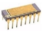
ICGOO电子元器件商城为您提供6N140A由Avago Technologies设计生产,在icgoo商城现货销售,并且可以通过原厂、代理商等渠道进行代购。 6N140A价格参考。Avago Technologies6N140A封装/规格:光隔离器 - 晶体管,光电输出, 光隔离器 达林顿晶体管 输出 1500VDC 4 通道 16-DIP。您可以下载6N140A参考资料、Datasheet数据手册功能说明书,资料中有6N140A 详细功能的应用电路图电压和使用方法及教程。
| 参数 | 数值 |
| 产品目录 | |
| 描述 | OPTOISO 1.5KV 4CH DARLNG 16-DIP逻辑输出光电耦合器 4Ch 1500%CTR Hermetically sealed |
| 产品分类 | |
| 品牌 | Avago Technologies |
| 产品手册 | http://www.avagotech.com/pages/en/optocouplers_hermetic/high_gain_four_channel/6n140a/ |
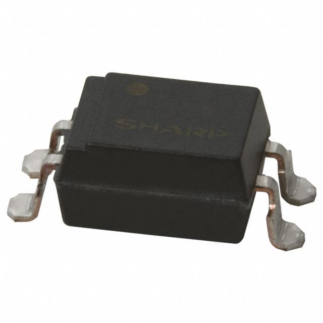
| 产品图片 |
|
| rohs | 符合RoHS无铅 / 符合限制有害物质指令(RoHS)规范要求 |
| 产品系列 | 光耦合器/光电耦合器,逻辑输出光电耦合器,Avago Technologies 6N140A- |
| 数据手册 | http://www.avagotech.com/docs/AV02-1766EN |
| 产品型号 | 6N140A |
| Vce饱和值(最大值) | 110mV |
| 上升/下降时间(典型值) | - |
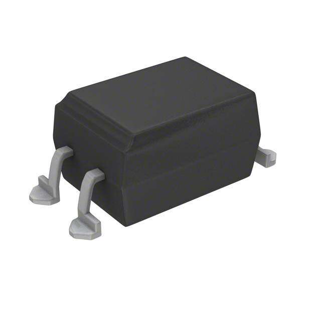
| 产品目录绘图 |
|
| 产品目录页面 | |
| 产品种类 | 逻辑输出光电耦合器 |
| 供应商器件封装 | 16-DIP |
| 其它名称 | 516-1834-5 |
| 包装 | 管件 |
| 商标 | Avago Technologies |
| 安装类型 | 通孔 |
| 封装/外壳 | 16-DIP(0.300",7.62mm) |
| 封装/箱体 | PDIP-16 |
| 工作温度 | -55°C ~ 125°C |
| 工厂包装数量 | 1 |
| 打开/关闭时间(典型值) | 2µs, 8µs |
| 最大传播延迟时间 | 100 us |
| 最大功率耗散 | 200 mW |
| 最大反向二极管电压 | 5 V |
| 最大工作温度 | + 125 C |
| 最大正向二极管电压 | 1.8 V |
| 最大正向二极管电流 | 5 mA |
| 最大连续输出电流 | 40 mA |
| 最小工作温度 | - 55 C |
| 标准包装 | 1 |
| 每芯片的通道数量 | 4 Channels |
| 电压-正向(Vf)(典型值) | 1.4V |
| 电压-输出(最大值) | 20V |
| 电压-隔离 | 1500VDC |
| 电流-DC正向(If) | 10mA |
| 电流-输出/通道 | 40mA |
| 电流传输比(最大值) | - |
| 电流传输比(最小值) | 200% @ 5mA |
| 电流传递比 | 1500 % |
| 输入类型 | DC |
| 输出类型 | Open Collector |
| 通道数 | 4 |
| 逻辑门类型 | Inverter |
| 配置 | 4 Channel |


.jpg)

- 商务部:美国ITC正式对集成电路等产品启动337调查
- 曝三星4nm工艺存在良率问题 高通将骁龙8 Gen1或转产台积电
- 太阳诱电将投资9.5亿元在常州建新厂生产MLCC 预计2023年完工
- 英特尔发布欧洲新工厂建设计划 深化IDM 2.0 战略
- 台积电先进制程称霸业界 有大客户加持明年业绩稳了
- 达到5530亿美元!SIA预计今年全球半导体销售额将创下新高
- 英特尔拟将自动驾驶子公司Mobileye上市 估值或超500亿美元
- 三星加码芯片和SET,合并消费电子和移动部门,撤换高东真等 CEO
- 三星电子宣布重大人事变动 还合并消费电子和移动部门
- 海关总署:前11个月进口集成电路产品价值2.52万亿元 增长14.8%

PDF Datasheet 数据手册内容提取
6N140A, HCPL-675x, 83024, HCPL-570x, HCPL-177K, 5962-89810, HCPL-573x, 1 HCPL-673x, 5962-89785, 5962-98002 Hermetically Sealed, Low I , Wide V , High Gain F CC Optocouplers Data Sheet Description Features These units are single, dual, and quad channel, hermetically Dual marked with device part number and DLA Standard sealed optocouplers. The products are capable of operation Microcircuit Drawing (SMD) and storage over the full military temperature range and can Manufactured and tested on a MIL-PRF-38534 Certified be purchased as either commercial product or with full Line MIL-PRF-38534 Class Level H or K testing or from the QML-38534, Class H and K appropriate DLA Standard Microcircuit Drawing (SMD). All Five hermetically sealed package configurations devices are manufactured and tested on a MIL-PRF-38534 certified line, and Class H and K devices are included in the DLA Performance guaranteed over full military temperature range: –55°C to +125°C Qualified Manufacturers List QML-38534 for Hybrid Microcircuits. Low input current requirement: 0.5 mA Each channel contains a GaAsP light emitting diode that is High current transfer ratio: 1500% typical at IF = 0.5 mA optically coupled to an integrated high gain photon detector. Low output saturation voltage: 0.11V typical The high gain output stage features an open collector output, 1500 Vdc withstand test voltage providing both lower saturation voltage and higher signaling High radiation immunity speed than possible with conventional photo-Darlington 6N138/9, HCPL-2730/31 function compatibility optocouplers. The shallow depth and small junctions offered Reliability data by the IC process provides better radiation immunity than conventional photo transistor optocouplers. Applications The supply voltage can be operated as low as 2.0V without adversely affecting the parametric performance. Military and aerospace These devices have a 300% minimum CTR at an input current High reliability systems of only 0.5 mA making them ideal for use in low input current Microprocessor system interface applications such as MOS, CMOS, low power logic interfaces or Transportation, medical, and life critical systems line receivers. Compatibility with high-voltage CMOS logic Isolated input line receiver systems is assured by specifying I and I at 18 Volts. CCH OH EIA RS-232-C line receiver Voltage level shifting Isolated input line receiver Isolated output line driver CAUTION It is advised that normal static precautions be Logic ground isolation taken in handling and assembly of this Harsh industrial environments component to prevent damage and/or Current loop receiver degradation which may be induced by ESD. System test equipment isolation Process control input/output isolation 1. See Selection Guide–Package Styles and Lead Configuration Options for available extensions. Broadcom - 1 -
6N140A, HCPL-675x, 83024, HCPL-570x, HCPL-177K, 5962-89810, HCPL-573x, HCPL-673x, Functional Diagram 5962-89785, 5962-98002 Data Sheet Functional Diagram Package styles for these parts are 8-pin and 16-pin DIP through hole (case outlines P and E respectively), 16-pin DIP flat pack Multiple channel devices available. (case outline F), and leadless ceramic chip carrier (case outline 2). Devices may be purchased with a variety of lead bend and plating options. See Selection Guide–Package Styles and Lead 1 8 Configuration Options for details. Standard Military Drawing (SMD) parts are available for each package and lead style. 2 7 Because the same electrical die (emitters and detectors) are used for each channel of each device listed in this data sheet, 3 6 absolute maximum ratings, recommended operating conditions, electrical specifications, and performance characteristics shown in the figures are similar for all parts 4 5 except as noted. Additionally, the same package assembly processes and materials are used in all devices. These similarities justify the use of a common data base for die Truth Table related reliability and certain limited radiation test results. (Positive Logic) Input Output On (H) L Off (L) H NOTE The connection of a 0.1-μF bypass capacitor between V and GND is recommended. CC Selection Guide–Package Styles and Lead Configuration Options Package 16-pin DIP 8-pin DIP 8-pin DIP 16-pin Flat Pack 20-Pad LCCC Lead Style Through Hole Through Hole Through Hole Unformed Leads Surface Mount Channels 4 1 2 4 2 Common Channel Wiring V , GND None V , GND V , GND None CC CC CC Part Number and Options Commercial 6N140A HCPL-5700 HCPL-5730 HCPL-6750 HCPL-6730 MIL-PRF-38534 Class H 6N140A/883B HCPL-5701 HCPL-5731 HCPL-6751 HCPL-6731 MIL-PRF-38534 Class K HCPL-177K HCPL-570K HCPL-573K HCPL-675K HCPL-673K Standard Lead Finish Gold Platea Gold Platea Gold Platea Gold Platea Solder Padsb Solder Dippedb Option #200 Option #200 Option #200 Butt Cut/Gold Platea Option #100 Option #100 Option #100 Gull Wing/Solderedb Option #300 Option #300 Option #300 Crew Cut/Gold Platea Option #600 Option #600 Option #600 Class H SMD Part Number Prescript for all below None 5962- 5962- None 5962- Gold Platea 8302401EC 8981001PC 8978501PC 8302401FC Solder Dippedb 8302401EA 8981001PA 8978501PA 89785022A Broadcom - 2 -
6N140A, HCPL-675x, 83024, HCPL-570x, HCPL-177K, 5962-89810, HCPL-573x, HCPL-673x, Functional Diagrams 5962-89785, 5962-98002 Data Sheet Package 16-pin DIP 8-pin DIP 8-pin DIP 16-pin Flat Pack 20-Pad LCCC Butt Cut/Gold Platea 8302401YC 8981001YC 8978501YC Butt Cut/Solderedb 8302401YA 8981001YA 8978501YA Gull Wing/Solderedb 8302401XA 8981001XA 8978501ZA Crew Cut/Gold Platea 8302401ZC Crew Cut/Solderedb 8302401ZA Class K SMD Part Number Prescript for all below 5962- 5962- 5962- 5962- 5962- Gold Platea 9800201KEC 8981002KPC 8978503KPC 9800201KFC Solder Dippedb 9800201KEA 8981002KPA 8978503KPA 8978504K2A Butt Cut/Gold Platea 9800201KYC 8981002KYC 8978503KYC Butt Cut/Solderedb 9800201KYA 8981002KYA 8978503KYA Gull Wing/Solderedb 9800201KXA 8981002KXA 8978503KZA Crew Cut/Gold Platea 9800201KZC Crew Cut/Solderedb 9800201KZA a. Gold Plate lead finish: Maximum gold thickness of leads is <100 micro inches. Typical is 60 to 90 micro inches. b. Solder lead finish: Sn63/Pb37. Functional Diagrams 16-pin DIP 8-pin DIP 8-pin DIP 16-pin Flat Pack 20-Pad LCCC Through Hole Through Hole Through Hole Unformed Leads Surface Mount 4 Channels 1 Channel 2 Channels 4 Channels 2 Channels 15 1 16 1 8 1 8 1 16 VCC2 VO2 19 13 2 15 2 7 2 7 2 1155 20 GND2 12 3 14 3 6 3 6 3 1144 2 VCC1 10 3 4 13 4 5 4 5 4 1133 GND1 VO1 7 8 5 12 5 12 6 11 6 11 7 10 7 10 8 9 8 9 NOTE All DIP and flat pack devices have common V and ground. LCCC (leadless ceramic chip carrier) package has CC isolated channels with separate V and ground connections. All diagrams are top view. CC Broadcom - 3 -
6N140A, HCPL-675x, 83024, HCPL-570x, HCPL-177K, 5962-89810, HCPL-573x, HCPL-673x, Leaded Device Marking 5962-89785, 5962-98002 Data Sheet Leaded Device Marking Leadless Device Marking Avago LOGO A QYYWWZ COMPLIANCE INDICATOR,[1] Avago LOGO A QYYWWZ COMPLIANCE INDICATOR,[1] Avago P/N XXXXXX DATE CODE, SUFFIX (IF NEEDED) Avago P/N XXXXXX DATE CODE, SUFFIX (IF NEEDED) DLA SMD[1] XXXXXXX PIN ONE/ X XXXX DLA SMD[1] DLA SMD[1] XXX XXX COUNTRY OF MFR. ESD IDENT XXXXXX DLA SMD[1] PIN ONE/ X 50434 Avago CAGE CODE[1] COUNTRY OF MFR. XXX 50434 Avago CAGE CODE[1] ESD IDENT [1] QML PARTS ONLY [1] QML PARTS ONLY Outline Drawings 16-Pin DIP Through Hole, 4 Channels 20.06 (0.790) 8.13 (0.320) 20.83 (0.820) MAX. 0.89 (0.035) 1.65 (0.065) 4.45 (0.175) MAX. 0.51 (0.020) MIN. 3.81 (0.150) 0.20 (0.008) MIN. 0.33 (0.013) 7.36 (0.290) 2.29 (0.090) 0.51 (0.020) 7.87 (0.310) 2.79 (0.110) MAX. Note: Dimensions in millimeters (inches). 16-Pin Flat Pack, 4 Channels 7.24 (0.285) 6.99 (0.275) 2.29 (0.090) MAX. 1.27 (0.050) REF. 11.13 (0.438) 10.72 (0.422) 0.46 (0.018) 0.36 (0.014) 8.13 (0.320) 2.84 (0.112) MAX. MAX. 0.88 (0.0345) 0.30 (0.012) MIN. 0.23 (0.009) 0.89 (0.035) 5.23 0.69 (0.027) (0.206) 9.14 (0.360) 8.64 (0.340) MAX. Note: Dimensions in millimeters (inches). Broadcom - 4 -
6N140A, HCPL-675x, 83024, HCPL-570x, HCPL-177K, 5962-89810, HCPL-573x, HCPL-673x, Outline Drawings 5962-89785, 5962-98002 Data Sheet 20-Terminal LCCC Surface Mount, 2 Channels 8.69 (0.342) 9.09 (0.358) 4.95 (0.195) 5.21 (0.205) 1.78 (0.070) 1.02 (0.040) (3 PLCS) 2.03 (0.080) 1.14 (0.045) 1.40 (0.055) 8.69 (0.342) 9.09 (0.358) 4.95 (0.195) TERMINAL 1 IDENTIFIER 5.21 (0.205) 2.16 (0.085) METALIZED 1.78 (0.070) CASTILLATIONS (20 PLCS) 2.03 (0.080) 0.64 (0.025) 0.51 (0.020) (20 PLCS) 1.52 (0.060) 2.03 (0.080) Note: Dimensions in millimeters (inches). Solder Thickness 0.127 (0.005) Max. 8-Pin DIP Through Hole, 1 and 2 Channel 10.03 (0.395) 8.13 (0.320) 10.29 (0.405) MAX. 1.02 (0.040) 7.16 (0.282) 1.52 (0.060) 7.57 (0.298) 4.32 (0.170) MAX. 0.51 (0.020) 3.81 (0.150) MIN. MIN. 0.20 (0.008) 0.33 (0.013) 7.36 (0.290) 2.29 (0.090) 0.51 (0.020) 7.87 (0.310) 2.79 (0.110) MAX. Note: Dimensions in millimeters (inches). Broadcom - 5 -
6N140A, HCPL-675x, 83024, HCPL-570x, HCPL-177K, 5962-89810, HCPL-573x, HCPL-673x, Hermetic Optocoupler Options 5962-89785, 5962-98002 Data Sheet Hermetic Optocoupler Options Option Description 100 Surface-mountable hermetic optocoupler with leads trimmed for butt joint assembly. This option is available on Commercial, Class H, and Class K product in 8-pin and 16-pin DIP. 4.32 (0.170) MAX. 0.51 (0.020) 1.14 (0.045) MIN. 1.40 (0.055) 2.29 (0.090) 0.51 (0.020) 2.79 (0.110) MAX. 4.32 (0.170) MAX. 0.51 (0.020) 1.14 (0.045) MIN. 1.40 (0.055) 0.20 (0.008) 0.33 (0.013) 2.29 (0.090) 0.51 (0.020) 2.79 (0.110) MAX. 7.36 (0.290) 7.87 (0.310) Note: Dimensions in millimeters (inches). 200 Lead finish is solder dipped rather than gold plated. This option is available on Commercial, Class H, and Class K product in 8-pin and 16-pin DIP. DLA Drawing (SMD) part numbers contain provisions for lead finish. All leadless chip carrier devices are delivered with solder-dipped terminals as a standard feature. 300 Surface-mountable hermetic optocoupler with leads cut and bent for gull wing assembly. This option is available on Commercial, Class H, and Class K product in 8-pin and 16-pin DIP. This option has solder-dipped leads. 4.57 (0.180) MAX. 0.51 (0.020) 1.40 (0.055) MIN. 1.65 (0.065) 2.29 (0.090) 0.51 (0.020) 2.79 (0.110) MAX. 4.57 (0.180) 4.57 (0.180) MAX. MAX. 0.20 (0.008) 0.51 (0.020) 1.40 (0.055) 5° MAX. 0.33 (0.013) MIN. 1.65 (0.065) 1.07 (0.042) 2.29 (0.090) 0.51 (0.020) 9.65 (0.380) 1.32 (0.052) 2.79 (0.110) MAX. 9.91 (0.390) Note: Dimensions in millimeters (inches). 600 Surface-mountable hermetic optocoupler with leads trimmed for butt joint assembly. This option is available on Commercial, Class H, and Class K product in 8-pin and 16-pin DIP. Contact factory for the availability of this option on DLA part types. 3.81 (0.150) 3.81 (0.150) MMAINX.. MAX. 0.20 (0.008) 0.51 (0.020) 0.33 (0.013) 0.51 (0.020) MIN. MIN. 2.29 (0.090) 1.14 (0.045) 2.79 (0.110) 1.25 (0.049) 7.36 (0.290) 2.29 (0.090) 1.02 (0.040) 7.87 (0.310) 2.79 (0.110) TYP. Note: Dimensions in millimeters (inches). Broadcom - 6 -
6N140A, HCPL-675x, 83024, HCPL-570x, HCPL-177K, 5962-89810, HCPL-573x, HCPL-673x, Absolute Maximum Ratings 5962-89785, 5962-98002 Data Sheet Absolute Maximum Ratings Parameter Symbol Min Max Unit Notes Storage Temperature T –65 +150 °C S Operating Temperature T –55 +125 °C A Case Temperature T — +170 °C C Junction Temperature T — +175 °C J Lead Solder Temperature — 260 for 10 sec °C Output Current (each channel) I — 40 mA O Output Voltage (each channel) VO –0.5 20 V a Supply Voltage V –0.5 20 V a CC Output Power Dissipation (each channel) — 50 mW b Peak Input Current (each channel, <1 ms duration) — 20 mA Average Input Current (each channel) IF — 10 mA c Reverse Input Voltage (each channel) V — 5 V R Package Power Dissipation (each channel) P — 200 mW D a. GND pin should be the most negative voltage at the detector side. Keeping V as low as possible, but greater than 2.0V, provides the lowest total I over CC OH temperature. b. Output power is collector output power plus total supply power for the single-channel device. For the dual-channel device, output power is collector output power plus one half the total supply power. For the quad-channel device, output power is collector output power plus one fourth of total supply power. Derate at 1.66 mW/°C above 110°C. c. Derate I at 0.33 mA/°C above 110°C. F 8-Pin Ceramic DIP Single Channel Schematic VCC 8 2 IF ICC ANODE + VF – IO 6 CATHODE 3 VO 5 GND ESD Classification (MIL-STD-883, Method 3015) HCPL-5700/01/0K and 6730/31/3K , Class 2 6N140A, 6N140A/883B, HCPL-177K, HCPL-6750/51/5K and HCPL-5730/31/3K , Class 3 Recommended Operating Conditions Parameter Symbol Min Max Unit Input Voltage, Low Level (Each Channel) V — 0.8 V F(OFF) Input Current, High Level (Each Channel) I 0.5 5 mA F(ON) Supply Voltage V 2.0 18 V CC Output Voltage V 2.0 18 V O Broadcom - 7 -
6N140A, HCPL-675x, 83024, HCPL-570x, HCPL-177K, 5962-89810, HCPL-573x, HCPL-673x, Electrical Characteristics 5962-89785, 5962-98002 Data Sheet Electrical Characteristics T = –55°C to +125°C, unless otherwise specified. A Limits Group Aa Parameter Symbol Test Conditions Unit Fig Notes Subgroup Min Typb Max Current Transfer Ratio CTR IF = 0.5 mA, VO = 0.4V, 1, 2, 3 300 1500 — % 3 c, d V = 4.5V CC I = 1.6 mA, V = 0.4V, 300 1000 — F O V = 4.5 V CC I =5 mA, V = 0.4V, 200 500 — F O V = 4.5V CC Logic Low Output Voltage VOL IF = 0.5 mA, IOL = 1.5 mA, 1, 2, 3 — 0.11 0.4 V 2 c V = 4.5V CC IF = 1.6 mA, IOL = 4.8 mA, — 0.13 0.4 c, e V = 4.5V CC IF =5 mA, IOL = 10 mA, — 0.16 0.4 c V = 4.5V CC Logic High Output Current IOH IF =2 μA, VO = 18V, 1, 2, 3 — 0.001 250 μA c V = 18V I CC 250 μA c, f OHX I I = 1.6 mA, V = 18V 1, 2, 3 — 1.0 2 mA g Logic Low Supply Single Channel CCL F CC Current and LCCC I = I = 1.6 mA, — 1.0 4 4 Dual Channel F1 F2 V = 18V CC I = I = I = I = 1.6 mA, — 1.7 4 Quad Channel F1 F2 F3 F4 V = 18V CC I I = 0 mA, V = 18V 1, 2, 3 — 0.001 20 μA g Logic High Supply Single Channel CCH F CC Current and LCCC I = I = 0 mA, — 40 Dual Channel F1 F2 V = 18V CC I = I = I = I = 0 mA, — 40 Quad Channel F1 F2 F3 F4 V = 18V CC V I = 1.6 mA 1 1.0 1.4 1.7 V 1 c Input Forward Voltage Single and Dual F F Channel 2 — — 1.7 3 — — 1.8 1, 2, 3 1.0 1.4 1.8 LCCC 1, 2 — 1.4 1.7 Quad Channel 3 — — 1.8 Input Reverse Breakdown Voltage BVR IR = 10 μA 1, 2, 3 5 — — V c Input-Output Insulation Leakage Current II-O ≤65% Relative Humidity 1 — — 1.0 μA h, i T = 25°C, t = 5s, A V = 1500 VDC I-O Broadcom - 8 -
6N140A, HCPL-675x, 83024, HCPL-570x, HCPL-177K, 5962-89810, HCPL-573x, HCPL-673x, Electrical Characteristics 5962-89785, 5962-98002 Data Sheet Limits Group Aa Parameter Symbol Test Conditions Unit Fig Notes Subgroup Min Typb Max Capacitance Between Input-Output CI-O f = 1 MHz, TA = 25°C 4 — — 4 pF c, j k, l Propagation Delay Time to Logic Low at t I = 0.5 mA, R = 4.7 kΩ, 9, 10, 11 — 30 100 μs 5, 6, c PHL F L Output V = 5V 7, 8 CC IF = 1.6 mA, RL = 1.5 kΩ, 9, 10, 11 — 5 30 c, e V = 5V CC IF =5 mA, RL = 680Ω, 9 — 2 5 c, l V = 5V CC 10, 11 10 9, 10, 11 10 c, e Propagation Delay Time to Logic High at t I = 0.5 mA, R = 4.7 kΩ, 9, 10, 11 — 17 60 μs 5, 6, c PLH F L Output V = 5V 7, 8 CC IF = 1.6 mA, RL = 1.5 kΩ, 9, 10, 11 — 14 50 c, e V = 5 V CC IF = 5 mA, RL = 680 Ω, 9 — 8 20 c, l V = 5V CC 10, 11 30 9, 10, 11 30 c, e Common Mode Transient Immunity at |CML| VCC = 5V, IF = 1.6 mA 9, 10, 11 500 1000 V/μs 9 c, m, n, R =1.5 kΩ, |V | = 25V l o Low Output Level L CM P-P |V | = 50 V e CM P-P Common Mode Transient Immunity at |CMH| VCC = 5V, IF =0 mA 9, 10, 11 500 1000 V/μs 9 c, m, n, R =1.5 kΩ, |V | = 25V l o High Output Level L CM P-P |V | = 50 V e CM P-P a. Commercial parts receive 100% testing at 25°C (Subgroups 1 and 9). SMD, Class H and Class K parts receive 100% testing at 25, 125, and –55°C (Subgroups 1 and 9, 2 and 10, 3 and 11, respectively). b. All typical values are at V = 5V, T = 25°C. CC A c. Each channel. d. Current Transfer Ratio is defined as the ratio of output collector current, I , to the forward LED input current, I , times 100%. O F e. Not required for 6N140A, 6N140A/883B, HCPL-177K, HCPL-6750/51/5K, 8302401, and 5962-9800201 types. f. I is the leakage current resulting from channel-to-channel optical crosstalk. I = 2 μA for channel under test. For all other channels, I = 10 mA. OHX F F g. The HCPL-6730, HCPL-6731, and HCPL-673K dual-channel parts function as two independent single channel units. Use the single channel parameter limits. h. All devices are considered two-terminal devices; measured between all input leads or terminals shorted together and all output leads or terminals shorted together. i. This is a momentary withstand test, not an operating condition. j. Measured between each input pair shorted together and all output connections for that channel shorted together. k. Parameters tested as part of device initial characterization and after design and process changes. Parameters guaranteed to limits specified for all lots not specifically tested. l. Required for 6N140A, 6N140A/883B, HCPL-177K, HCPL-6750/51/5K, 8302401, and 5962-9800201 types. m. CM is the maximum rate of rise of the common mode voltage that can be sustained with the output voltage in the logic low state (V < 0.8 V). CM is the L O H maximum rate of fall of the common mode voltage that can be sustained with the output voltage in the logic high state (V > 2.0 V). O Broadcom - 9 -
6N140A, HCPL-675x, 83024, HCPL-570x, HCPL-177K, 5962-89810, HCPL-573x, HCPL-673x, Typical Characteristics 5962-89785, 5962-98002 Data Sheet n. In applications where dV/dt may exceed 50,000 V/μs (such as a static discharge), a series resistor, R , should be included to protect the detector ICs from CC destructively high surge currents. The recommended value is: For single channel: 1 (V) R = ----------------------------- kΩ CC 0.15 I (mA) F For dual channel: 1 (V) R = -------------------------- kΩ CC 0.3 I (mA) F For quad channel: 1 (V) R = -------------------------- kΩ CC 0.6 I (mA) F o. Parameters tested as part of device initial characterization and after design and process changes. Parameters guaranteed to limits specified for all lots not specifically tested. Typical Characteristics T = 25°C, V = 5V. A CC Parameter Symbol Typ Unit Test Conditions Note Input Capacitance C 60 pF V = 0V, f = 1 MHz a IN F Input Diode Temperature Coefficient ΔV /ΔT –1.8 mV/°C I = 1.6 mA a F A F Resistance (Input-Output) RI-O 1012 Ω VI-O = 500V a, b Capacitance (Input-Output) CI-O 2.0 pF f = 1 MHz a, b Dual and Quad Channel Product Only Input-Input Leakage Current I 0.5 nA Relative Humidity = ≤65%, c I-I V = 500V, t = 5s I-I Resistance (Input-Input) RI-I 1012 Ω VI-I = 500V c Capacitance (Input-Input) C 1.0 pF f = 1 MHz c I-I a. Each channel. b. Measured between each input pair shorted together and all output connections for that channel shorted together. c. Measured between adjacent input pairs shorted together for each multichannel device. Broadcom - 10 -
6N140A, HCPL-675x, 83024, HCPL-570x, HCPL-177K, 5962-89810, HCPL-573x, HCPL-673x, Typical Characteristics 5962-89785, 5962-98002 Data Sheet Figure1 Input Diode Forward Current vs. Forward Voltage Figure2 Normalized DC Transfer Characteristics Figure3 Normalized Current Transfer Ratio vs. Input Diode Figure4 Normalized Supply Current vs. Input Diode Forward Forward Current Current Figure5 Propagation Delay to Logic Low vs. Input Pulse Period Figure6 Propagation Delay vs. Temperature Broadcom - 11 -
6N140A, HCPL-675x, 83024, HCPL-570x, HCPL-177K, 5962-89810, HCPL-573x, HCPL-673x, Typical Characteristics 5962-89785, 5962-98002 Data Sheet Figure7 Propagation Delay vs. Input Diode Forward Current Figure9 Test Circuit for Transient Immunity and Typical Waveforms IF B RCC* 56 (cid:58) +5 V 1 8 1.0 (cid:80)F RL A 2 7 VO 3 6 VFF 4 5 VCM + – PULSE GEN. * See note n on page 10. Figure8 Switching Test Circuit PULSE GEN. ZO = 50 (cid:58) tr, tf = 50 ns RCC* 56 (cid:58) f = 100 Hz IF +5 V tPULSE = 0.5ms 1 8 1.0 (cid:80)F RL IF MONITOR 2 7 VO Rm 3 6 CL** 4 5 Figure10 Recommended Drive Circuitry Using TTL Open-Collector Logic * See note n on page 10. VCC ** CL includes probe and stray wiring capacitance. R 1 ILEAK R 2 1 8 R2 (cid:116)2.4I –F VF 2 7 R1 (cid:100)VCCI F– + V FI L–EA IKF R2 3 6 4 5 R2 MAY BE OMITTED IF ADDITIONAL FANOUT IS NOT USED. Broadcom - 12 -
6N140A, HCPL-675x, 83024, HCPL-570x, HCPL-177K, 5962-89810, HCPL-573x, HCPL-673x, Typical Characteristics 5962-89785, 5962-98002 Data Sheet Figure11 Operating Circuit for Burn-In and Steady State Life Tests VCC + 18 V 1 8 VOC (EACH INPUT) 2 7 0.01 (cid:80)F + – 3 6 VIN 4 5 (EACH OUTPUT) CONDITIONS: IF = 10 mA IO = 40 mA TA = +125°C * ALL CHANNELS TESTED SIMULTANEOUSLY. Broadcom - 13 -
For product information and a complete list of distributors, please go to our web site: www.broadcom.com. Broadcom, the pulse logo, Connecting everything, Avago Technologies, Avago, and the A logo are among the trademarks of Broadcom in the United States, certain other countries and/or the EU. Copyright © 2005-2018 Broadcom. All Rights Reserved. The term "Broadcom" refers to Broadcom Inc. and/or its subsidiaries. For more information, please visit www.broadcom.com. Broadcom reserves the right to make changes without further notice to any products or data herein to improve reliability, function, or design. Information furnished by Broadcom is believed to be accurate and reliable. However, Broadcom does not assume any liability arising out of the application or use of this information, nor the application or use of any product or circuit described herein, neither does it convey any license under its patent rights nor the rights of others. AV02-1766EN – May 4, 2018
Mouser Electronics Authorized Distributor Click to View Pricing, Inventory, Delivery & Lifecycle Information: B roadcom Limited: 5962-8978501PA 5962-8978501PC 5962-8978501YA 5962-8978501YC 5962-8978501ZA 5962-89785022A 5962- 8978503KPA 5962-8978503KPC 5962-8978504K2A 5962-8981001PA 5962-8981001PC 5962-8981001XA 5962- 8981001YA 5962-8981001YC 5962-8981002KPA 5962-8981002KPC 5962-9800201KEA 5962-9800201KEC 5962- 9800201KFC 6N140A 6N140A#100 6N140A#200 6N140A#300 6N140A/883B 6N140A/883B#100 6N140A/883B#200 6N140A/883B#300 6N140A/883B#600 6N140A-600 8302401EA 8302401EC 8302401FC 8302401XA 8302401YA 8302401YC 8302401ZA 8302401ZC HCPL-177K HCPL-177K#200 HCPL-177K-100 HCPL-177K-300 HCPL-177K-600 HCPL-5700 HCPL-5700#100 HCPL-5700#200 HCPL-5700#300 HCPL-5701 HCPL-5701#100 HCPL-5701#200 HCPL-5701#300 HCPL-570K HCPL-570K#200 HCPL-570K#300 HCPL-570K- 100 HCPL-5730 HCPL-5730#100 HCPL-5730#200 HCPL-5730#300 HCPL-5731 HCPL-5731#100 HCPL- 5731#200 HCPL-5731#300 HCPL-573K HCPL-573K#200 HCPL-573K#300 HCPL-573K-100 HCPL-6730 HCPL- 6731 HCPL-673K HCPL-6750 HCPL-6751 HCPL-675K 5962-9800201KXA 5962-9800201KYA 5962-9800201KYC 5962-9800201KZA 5962-9800201KZC 5962-8978503KYA 5962-8978503KYC 5962-8978503KZA 5962- 8981002KXA 5962-8981002KYA 5962-8981002KYC