ICGOO在线商城 > 隔离器 > 光隔离器 - 晶体管,光电输出 > 6N138-000E
/6N138-000E.jpg)
 Datasheet下载
- 型号: 6N138-000E
- 制造商: Avago Technologies
- 库位|库存: xxxx|xxxx
- 要求:
| 数量阶梯 | 香港交货 | 国内含税 |
| +xxxx | $xxxx | ¥xxxx |
查看当月历史价格
查看今年历史价格
6N138-000E产品简介:
ICGOO电子元器件商城为您提供6N138-000E由Avago Technologies设计生产,在icgoo商城现货销售,并且可以通过原厂、代理商等渠道进行代购。 6N138-000E价格参考¥4.45-¥12.45。Avago Technologies6N138-000E封装/规格:光隔离器 - 晶体管,光电输出, 光隔离器 有基极的达林顿晶体管 输出 3750Vrms 1 通道 8-DIP。您可以下载6N138-000E参考资料、Datasheet数据手册功能说明书,资料中有6N138-000E 详细功能的应用电路图电压和使用方法及教程。
| 参数 | 数值 |
| 产品目录 | |
| 描述 | OPTOISO 3.75KV DARL W/BASE 8DIP高速光耦合器 100 KBd 2500Vrms |
| 产品分类 | |
| 品牌 | Avago Technologies |
| 产品手册 | |
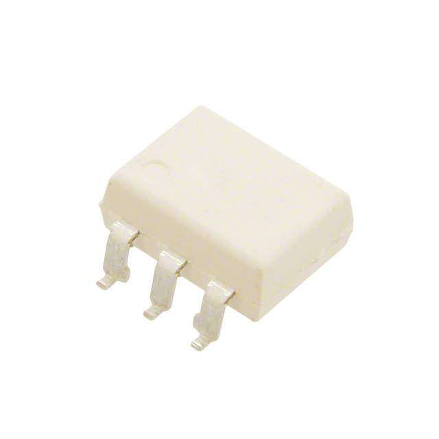
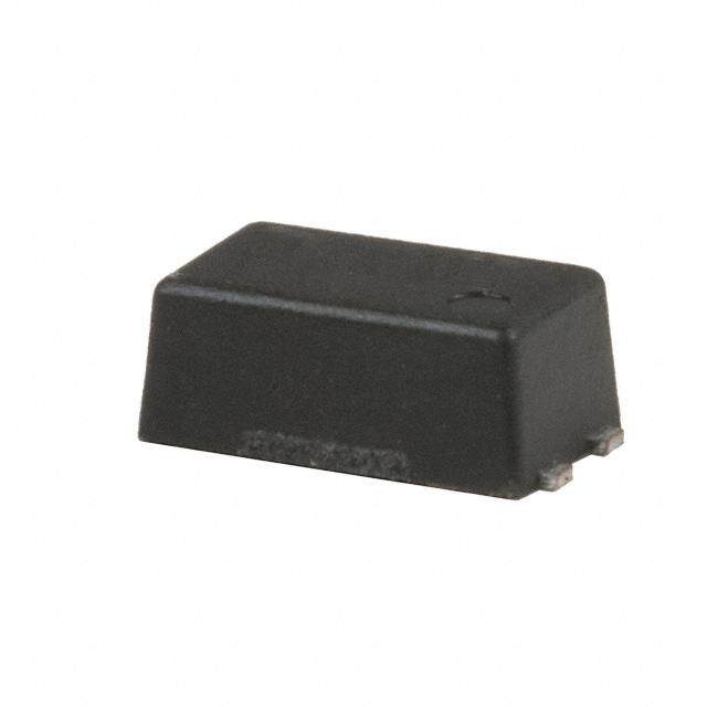
| 产品图片 |
|
| rohs | 符合RoHS无铅 / 符合限制有害物质指令(RoHS)规范要求 |
| 产品系列 | 光耦合器/光电耦合器,高速光耦合器,Avago Technologies 6N138-000E- |
| 数据手册 | http://www.avagotech.com/docs/AV02-1359EN |
| 产品型号 | 6N138-000E |
| PCN封装 | |
| Vce饱和值(最大值) | - |
| 上升/下降时间(典型值) | - |
| 上升时间 | 35 us |
| 下降时间 | 10 us |
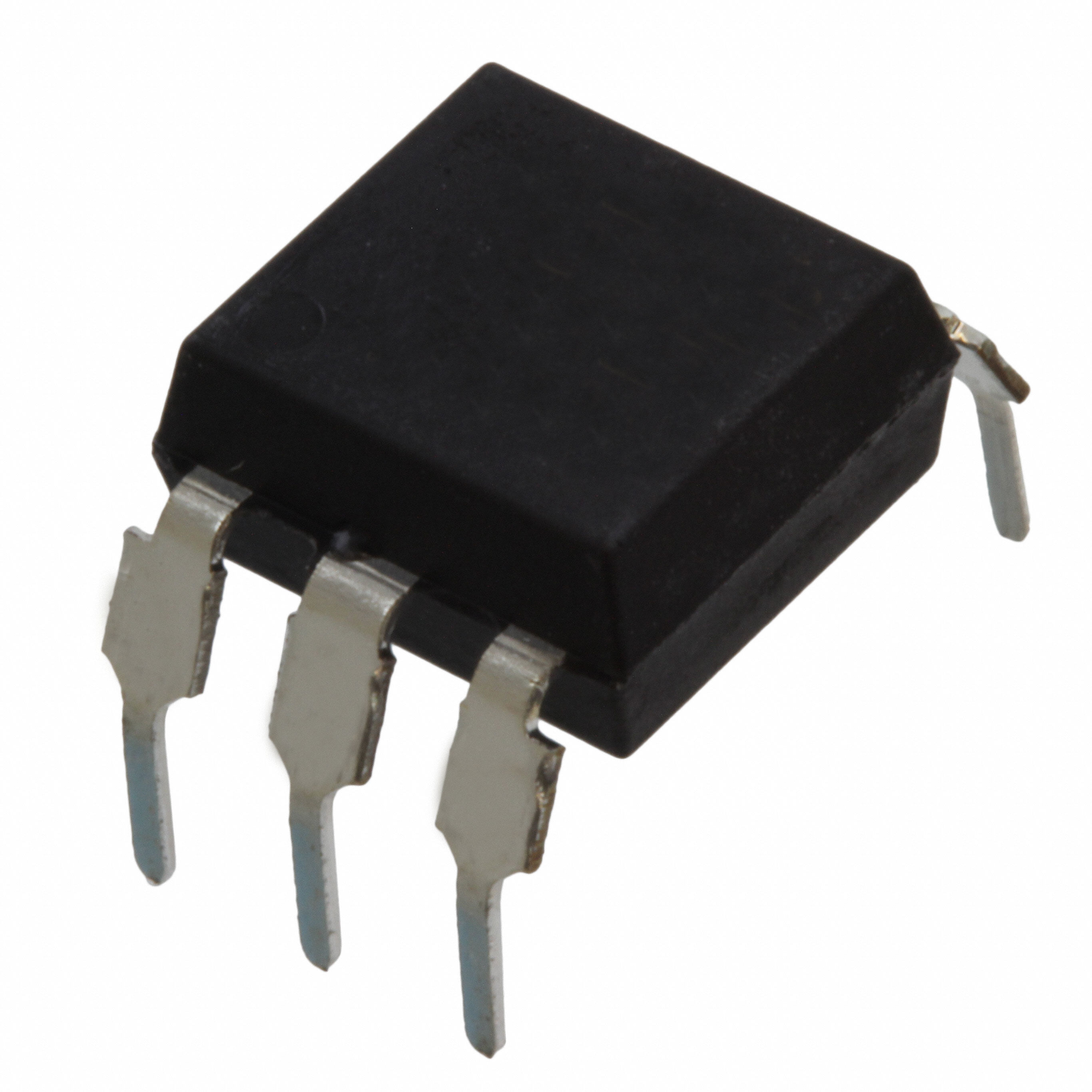
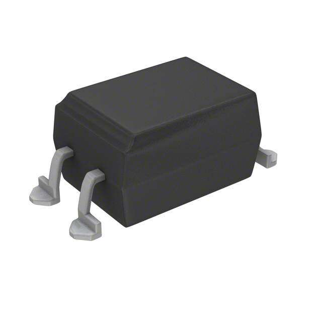
| 产品目录绘图 |
|
| 产品种类 | 高速光耦合器 |
| 供应商器件封装 | 8-DIP |
| 其它名称 | 516-1600-5 |
| 包装 | 管件 |
| 商标 | Avago Technologies |
| 安装类型 | 通孔 |
| 封装 | Tube |
| 封装/外壳 | 8-DIP(0.300",7.62mm) |
| 封装/箱体 | PDIP-8 |
| 工作温度 | -40°C ~ 85°C |
| 工厂包装数量 | 50 |
| 打开/关闭时间(典型值) | 1.6µs, 10µs |
| 数据速率 | 100 kBd |
| 最大功率耗散 | 135 mW |
| 最大反向二极管电压 | 5 V |
| 最大工作温度 | + 70 C |
| 最大正向二极管电压 | 1.7 V |
| 最大正向二极管电流 | 12 mA |
| 最小工作温度 | 0 C |
| 最小正向二极管电压 | 1.25 V |
| 标准包装 | 50 |
| 每芯片的通道数量 | 1 Channel |
| 电压-正向(Vf)(典型值) | 1.4V |
| 电压-输出(最大值) | 7V |
| 电压-隔离 | 3750Vrms |
| 电流-DC正向(If) | 20mA |
| 电流-输出/通道 | 60mA |
| 电流传输比(最大值) | 2600% @ 1.6mA |
| 电流传输比(最小值) | 300% @ 1.6mA |
| 电流传递比 | 1600 % |
| 绝缘电压 | 3750 Vrms |
| 输入类型 | DC |
| 输出类型 | 有基极的达林顿晶体管 |
| 输出设备 | Photodarlington |
| 通道数 | 1 |


.jpg)


- 商务部:美国ITC正式对集成电路等产品启动337调查
- 曝三星4nm工艺存在良率问题 高通将骁龙8 Gen1或转产台积电
- 太阳诱电将投资9.5亿元在常州建新厂生产MLCC 预计2023年完工
- 英特尔发布欧洲新工厂建设计划 深化IDM 2.0 战略
- 台积电先进制程称霸业界 有大客户加持明年业绩稳了
- 达到5530亿美元!SIA预计今年全球半导体销售额将创下新高
- 英特尔拟将自动驾驶子公司Mobileye上市 估值或超500亿美元
- 三星加码芯片和SET,合并消费电子和移动部门,撤换高东真等 CEO
- 三星电子宣布重大人事变动 还合并消费电子和移动部门
- 海关总署:前11个月进口集成电路产品价值2.52万亿元 增长14.8%
.jpg)
.jpg)

PDF Datasheet 数据手册内容提取
HCPL-0700, HCPL-0701, HCNW138, HCNW139, 6N139, 6N138, Low Input Current, High Gain Optocouplers Data Sheet Lead (Pb) Free RoHS 6 fully compliant RoHS 6 fully compliant options available; -xxxE denotes a lead-free product Description Features These high gain series couplers use a Light Emitting • High current transfer ratio – 2000% typical (4500 % Diode and an integrated high gain photodetec tor to typical for HCNW139/138) provide extremely high current transfer ratio between • Low input current requirements – 0.5 mA input and output. Separate pins for the photodiode • TTL compatible output – 0.1 V V typical OL and output stage result in TTL compatible saturation • Performance guaranteed over temperature 0°C voltages and high speed operation. Where desired the to 70°C V and V terminals may be tied together to achieve CC O • Base access allows gain bandwidth adjustment conven tional photodarlington operation. A base • High output current – 60 mA access terminal allows a gain bandwidth adjustment to be made. • Safetyapproval - UL recognized – 3750 V rms for 1 minute and 5000 V The 6N139, HCPL-0701, and HCNW139 are for use in rms* for 1 minute per UL 1577 CMOS, LSTTL or other low power appli ca tions. A 400% - CSA approved minimum current transfer ratio is guaranteed over 0 to 70°C - IEC/EN/DIN EN 60747-5-5 approved with V = IORM operating range for only 0.5 mA of LED current. 1414 V for HCNW139 and HCNW138 peak The 6N138, HCPL-0700, and HCNW138 are designed for • Available in 8-Pin DIP or SOIC-8 footprint or widebody use mainly in TTL applications. Current Transfer Ratio package (CTR) is 300% minimum over 0 to 70°C for an LED current • MIL-PRF-38534 hermetic version available of 1.6 mA (1 TTL Unit load ). A 300% minimum CTR (HCPL-5700/1) enables operation with 1 TTL Load using a 2.2 kΩ Applications pull-up resistor. • Ground isolate most logic families – TTL/TTL, CMOS/ Functional Diagram TTL, CMOS/CMOS, LSTTL/TTL, CMOS/LSTTL • Low input current line receiver NC 1 8 VCC • High voltage insulation (HCNW139/138) • EIA RS-232C line receiver TRUTH TABLE ANODE 2 7 VB LED VO • Telephone ring detector ON LOW • 117 V ac line voltage status indicator – low input CATHODE 3 6 VO OFF HIGH power dissipation • Low power systems – ground isolation NC 4 5 GND * 5000 V rms/1 minute rating is for HCNW139/138 and Option 020 (6N139/138) products only. A 0.1 µF bypass capacitor connected between pins 8 and 5 is recommended. CAUTION: It is advised that normal static precautions be taken in handling and assembly of this component to prevent damage and/or degradation which may be induced by ESD. The components featured in this datasheet are not to be used in military or aerospace applications or environments.
Selection for lower input current down to 250 µA is available upon request. The HCPL-0701 and HCPL-0700 are surface mount devices packaged in an industry standard SOIC-8 footprint. The SOIC-8 does not require “through holes” in a PCB. This package occupies approximately one-third the foot- print area of the standard dual-in-line package. The lead profile is designed to be compatible with standard surface mount processes. The HCNW139 and HCNW138 are packaged in a widebody encapsulation that provides creepa ge and clearance di- mensions suitable for safety approval by regulatory agencies worldwide. Selection Guide 8-Pin DIP Small Outline Widebody (300 Mil) SO-8 (400 mil) Hermetic Dual Single Dual Single and Dual Package Minimum Channel Channel Channel Channel Single Single Input ON Absolute Package Package Package Packages Channel Channel Current Minimum Maximum Package HCPL- HCPL- HCPL- Package (I) CTR V HCPL- F CC 6N139 2731[1] 0701 0731 HCNW139 0.5 mA 400% 18 V 6N138 2730[1] 0700 0730 HCNW138 1.6 mA 300% 7 V HCPL-4701[1] 4731[1] 070A[1] 073A[1] 40 µA 800% 18 V 0.5 mA 300% 20 V 5701[1] 5700[1] 5731[1] 5730[1] Note: 1. Technical data are on separate Avago publications. Schematic VCC 8 I CC 2 IF ANODE + V F – CATHODE 3 IO 6 VO 5 GND SHIELD IB 7 VB 2
Ordering Information 6N138, 6N139, HCPL-0700 and HCPL-0701 are UL Recognized with 3750 Vrms for 1 minute per UL1577 and are ap- proved under CSA Component Acceptance Notice #5, File CA 88324. Option UL 5000 Vrms/ Part RoHS non RoHS Surface Gull Tape 1 Minute IEC/EN/DIN Number Compliant Compliant Package Mount Wing & Reel rating EN 60747-5-5 Quantity 6N138 -000E no option 50 per tube 6N139 -300E #300 X X 50 per tube -500E #500 X X X 1000 per reel -020E #020 X 50 per tube 300 mil -320E #320 X X X 50 per tube DIP-8 -520E #520 X X X X 1000 per reel -060E #060 X 50 per tube -360E #360 X X X 50 per tube -560E #560 X X X X 1000 per reel HCPL-0700 -000E no option X 100 per tube HCPL-0701 -500E #500 X X 1500 per reel SO-8 -060E #060 X X 100 per tube -560E #560 X X X 1500 per reel HCNW138 -000E no option 42 per tube 400 mil HCNW139 -300E #300 Widebody X X 42 per tube DIP-8 -500E #500 X X X 750 per reel To order, choose a part number from the part number column and combine with the desired option from the option column to form an order entry. Example 1: 6N138-560E to order product of 300 mil DIP Gull Wing Surface Mount package in Tape and Reel packaging with IEC/EN/DIN EN 60747-5-5 Safety Approval and RoHS compliant. Example 2: HCPL-0700 to order product of 300 mil DIP package in Tube packaging and non RoHS compliant. Option datasheets are available. Contact your Avago sales representative or authorized distributor for information. Remarks: The notation ‘#XXX’ is used for existing products, while (new) products launched since July 15, 2001 and RoHS compliant will use ‘–XXXE.’ 3
Package Outline Drawings 8-Pin DIP Package (6N139/6N138)** 9.65 ± 0.25 7.62 ± 0.25 (0.380 ± 0.010) (0.300 ± 0.010) DEVICE PART NUMBER 8 7 6 5 6.35 ± 0.25 (0.250 ± 0.010) AVAGO A NNNN Z TEST RATING CODE • LEAD FREE YYWW UL LOGO EEE P SPECIAL PROGRAM CODE PIN 1 DOT 1 2 3 4 1.78 (0.070) MAX. 1.19 (0.047) MAX. DATE CODE LOT ID + 0.076 5° TYP. 0.254 - 0.051 + 0.003) 3.56 ± 0.13 4.70 (0.185) MAX. (0.010 - 0.002) (0.140 ± 0.005) 0.51 (0.020) MIN. DIMENSIONS IN MILLIMETERS AND (INCHES). 2.92 (0.115) MIN. * MARKING CODE LETTER FOR OPTION NUMBERS "L" = OPTION 020 OPTION NUMBERS 300 AND 500 NOT MARKED. 1.080 ± 0.320 0.65 (0.025) MAX. NOTE: FLOATING LEAD PROTRUSION IS 0.25 mm (10 mils) MAX. (0.043 ± 0.013) 2.54 ± 0.25 (0.100 ± 0.010) **JEDEC Registered Data. 8-Pin DIP Package with Gull Wing Surface Mount Option 300 (6N139/6N138) LAND PATTERN RECOMMENDATION 1.016 (0.040) 8 7 6 5 6.350 ± 0.25 (0.250 ± 0.010) 10.9 (0.430) 1 2 3 4 9.65 ± 0.25 (0.380 ± 0.010) 2.0 (0.080) 1.27 (0.050) 1.780 (0.070) 9.65 ± 0.25 1.19 MAX. (0.380 ± 0.010) (0.047) 7.62 ± 0.25 MAX. (0.300 ± 0.010) 0.254 + 0.076 - 0.051 3.56 ± 0.13 (0.010+ 0.003) (0.140 ± 0.005) - 0.002) 1.080 ± 0.320 0.635 ± 0.25 (0.043 ± 0.013) 0.635 ± 0.130 (0.025 ± 0.010) 2.54 (0.025 ± 0.005) 12° NOM. (0.100) BSC DIMENSIONS IN MILLIMETERS (INCHES). LEAD COPLANARITY = 0.10 mm (0.004 INCHES). NOTE: FLOATING LEAD PROTRUSION IS 0.25 mm (10 mils) MAX. 4
Small Outline SO-8 Package (HCPL-0701/HCPL-0700) LAND PATTERN RECOMMENDATION 8 7 6 5 TEST RATING DEVNICUEM PBAERRT NNNN Z CODE 5.994 ± 0.203 • (0.236 ± 0.008) (30..913575 ±± 00..102075) LEAD FREE YYWW DATE CODE 7.49 (0.295) EEE LOT ID PIN 1 DOT 1 2 3 4 1.9 (0.075) 0.406 ± 0.076 (0.016 ± 0.003) 1.270 BSC (0.050) 0.64 (0.025) * 5.080 ± 0.127 7° 0.432 45° X (0.200 ± 0.005) (0.017) 3.175 ± 0.127 (0.125 ± 0.005) 0 ~ 7° 0.228 ± 0.025 1.524 (0.009 ± 0.001) (0.060) 0.203 ± 0.102 * TOTAL PACKAGE LENGTH (INCLUSIVE OF MOLD FLASH) (0.008 ± 0.004) 5.207 ± 0.254 (0.205 ± 0.010) 0.305 MIN. (0.012) DIMENSIONS IN MILLIMETERS (INCHES). LEAD COPLANARITY = 0.10 mm (0.004 INCHES) MAX. NOTE: FLOATING LEAD PROTRUSION IS 0.15 mm (6 mils) MAX. 8-Pin Widebody DIP Package (HCNW139/HCNW138) 11.00 11.23 ± 0.15 MAX. (0.433) (0.442 ± 0.006) 9.00 ± 0.15 (0.354 ± 0.006) 8 7 6 5 AVAGO DEVICE PART A TEST RATING NUMBER NNNNNNNN Z CODE • LEAD FREE YYWW DATE CODE EEE LOT ID PIN 1 DOT 1 2 3 4 10.16 (0.400) TYP. 1.55 (0.061) 7° TYP. + 0.076 0.254 MAX. - 0.0051 + 0.003) (0.010 - 0.002) 5.10 MAX. (0.201) 3.10 (0.122) 3.90 (0.154) 0.51 (0.021) MIN. 2.54 (0.100) TYP. DIMENSIONS IN MILLIMETERS (INCHES). 1.80 ± 0.15 0.40 (0.016) (0.071 ± 0.006) 0.56 (0.022) NOTE: FLOATING LEAD PROTRUSION IS 0.25 mm (10 mils) MAX. 5
8-Pin Widebody DIP Package with Gull Wing Surface Mount Option 300 (HCNW139/HCNW138) LAND PATTERN RECOMMENDATION 8 7 6 5 13.56 9.00 ± 0.15 (0.534) (0.354 ± 0.006) 1 2 3 4 11.23 ± 0.15 1.3 2.29 (0.442 ± 0.006) (0.051) (0.09) 12.30 ± 0.30 1.55 (0.484 ± 0.012) (0.061) 11.00 MAX. MAX. (0.433) 4.00 MAX. (0.158) 1.80 ± 0.15 1.00 ± 0.15 (0.071 ± 0.006) 2.54 0.75 ± 0.25 (0.039 ± 0.006) 0.254 + 0.076 (0.100) (0.030 ± 0.010) - 0.0051 BSC + 0.003) (0.010 - 0.002) 7° NOM. DIMENSIONS IN MILLIMETERS (INCHES). LEAD COPLANARITY = 0.10 mm (0.004 INCHES). NOTE: FLOATING LEAD PROTRUSION IS 0.25 mm (10 mils) MAX. 6
Solder Reflow Profile Recommended reflow condition as per JEDEC Standard, J-STD-020 (latest revision). Non-Halide Flux should be used. Regulatory Information The 6N139/138, HCNW139/138, and HCPL-0701/0700 have been approved by the following organizations: UL Recognized under UL 1577, Component Recognition Program, File E55361. CSA Approved under CSA Component Acceptance Notice #5, File CA 88324. IEC/EN/DIN EN 60747-5-5 HCNW139/138 and Option 060/360/560 only Insulation and Safety Related Specifications Parameter Symbol 8-Pin DIP SO-8 Widebody Units Conditions (300 Mil) Value (400 Mil) Value Value Minimum External L(101) 7.1 4.9 9.6 mm Measured from input terminals to output Air Gap (External terminals, shortest distance through air. Clearance) Minimum External L(102) 7.4 4.8 10.0 mm Measured from input terminals to output Tracking (External terminals, shortest distance path along body. Creepage) Minimum Internal 0.08 0.08 1.0 mm Through insulation distance, conductor to Plastic Gap conductor, usually the direct distance be- (Internal Clearance) tween the photoemitter and photodetector inside the optocoupler cavity. Minimum Internal NA NA 4.0 mm Measured from input terminals to output Tracking (Internal terminals, along internal cavity. Creepage) Tracking Resistance CTI 200 200 200 Volts DIN IEC 112/VDE 0303 Part 1 (Comparative Tracking Index) Isolation Group IIIa IIIa IIIa Material Group (DIN VDE 0110, 1/89, Table 1) Option 300 - surface mount classification is Class A in accordance with CECC 00802. 7
IEC/EN/DIN EN 60747-5-5 Insulation Characteristics (HCNW139 and HCNW138) Description Symbol Characteristic Unit Installation classification per DIN VDE 0110, Table 1 for rated mains voltage ≤ 150 Vrms I – IV for rated mains voltage ≤ 300 Vrms I – IV for rated mains voltage ≤ 600 Vrms I – IV for rated mains voltage ≤ 1000 Vrms I – III Climatic Classification 0/70/21 Pollution Degree (DIN VDE 0110/39) 2 Maximum Working Insulation Voltage V 1414 V IORM peak Input to Output Test Voltage, Method b* V 2651 V PR peak V x 1.875 = V , 100% Production Test with t =1 sec, IORM PR m Partial discharge < 5 pC Input to Output Test Voltage, Method a* V 2262 V PR peak V x 1.6 = V , Type and Sample Test, t =10 sec, IORM PR m Partial discharge < 5 pC Highest Allowable Overvoltage (Transient Overvoltage t = 60 sec) V 8000 V ini IOTM peak Safety-limiting values – maximum values allowed in the event of a failure. Case Temperature T 150 °C S Input Current I 400 mA S, INPUT Output Power P 700 mW S, OUTPUT Insulation Resistance at T, V = 500 V R >109 Ω S IO S *Refer to the front of the optocoupler section of the current catalog, under Product Safety Regulations section, IEC/EN/DIN EN 60747-5-5, for a detailed description. Note: Isolation characteristics are guaranteed only within the safety maximum ratings which must be ensured by protective circuits in application. 8
Absolute Maximum Ratings* (No Derating Required up to 85°C) Parameter Symbol Min. Max. Units Storage Temperature T -55 125 °C S Operating Temperature** T -40 85 °C A Average Forward Input Current I 20 mA F(AVG) Peak Forward Input Current I 40 mA FPK (50% Duty Cycle, 1 ms Pulse Width) Peak Transient Input Current I 1.0 A F(TRAN) (<1 µs Pulse Width, 300 pps) Reverse Input Voltage V 5 V R HCNW139/138 3 V Input Power Dissipation P 35 mW I Output Current (Pin 6) I 60 mA O Emitter Base Reverse Voltage (Pin 5-7) V 0.5 V EB Supply Voltage and Output Voltage V -0.5 18 V CC (6N139, HCPL-0701, HCNW139) Supply Voltage and Output Voltage V -0.5 7 V CC (6N138, HCPL-0700, HCNW138) Output Power Dissipation P 100 mW O Total Power Dissipation P 135 mW T Lead Solder Temperature 260°C for 10 sec., 1.6 mm below seating plane (for Through Hole Devices) HCNW139/138 260°C for 10 sec., up to seating plane Reflow Temperature Profile See Package Outline Drawings section (for SOIC-8 and Option #300) *JEDEC Registered Data for 6N139 and 6N138. **0°C to 70°C on JEDEC Registration. Recommended Operating Conditions Parameter Symbol Min. Max. Units Power Supply Voltage V 4.5 18 V CC Forward Input Current (ON) I 0.5 12.0 mA F(ON) Forward Input Voltage (OFF) V 0 0.8 V F(OFF) Operating Temperature T 0 70 °C A 9
Electrical Specifications 0°C ≤ T ≤ 70°C, 4.5 V ≤ V ≤ 18 V, 0.5 mA ≤ I ≤ 12 mA, 0 V ≤ V ≤ 0.8 V, unless otherwise specified. A CC F(ON) F(OFF) All Typicals at T = 25°C. See Note 7. A Parameter Sym. Device Min. Typ.** Max. Units Test Conditions Fig. Note Current CTR 6N139 400* 2000 5000 % I = 0.5 mA V = 4.5 2, 3 1, 2, F CC Transfer HCPL-0701 VO = 0.4 V 4 Ratio HCNW139 400 4500 6N139 500* 1600 2600 I = 1.6 mA F HCPL-0701 HCNW139 500 3000 300 1600 I = 5.0 mA F 200 850 I = 12 mA F 6N138 300* 1600 2600 I = 1.6 mA F HCPL-0700 HCNW138 1500 Logic Low V 6N139 0.1 0.4 V I = 0.5 mA, V = 4.5 1 2 OL F CC Output HCPL-0701 I = 2 mA O Voltage HCNW139 I = 1.6 mA, F I = 8 mA O I = 5.0 mA, F I = 15 mA O 0.2 I = 12 mA, F I = 24 mA O 6N138 0.1 I = 1.6 mA, F HCPL-0700 I = 4.8 mA O HCNW138 Logic High I 6N139 0.05 100 µA V = V = 18 V I = 0 mA 2 OH O CC F Output HCPL-0701 Current HCNW139 6N138 0.1 250 V = V = 7 V O CC HCPL-0700 HCNW138 Logic Low I 6N138/139 0.4 1.5 mA I = 1.6 mA, V = Open, 10 2 CCL F O Supply HCPL-0701/0700 V = 18 V CC Current HCNW139 0.5 2 HCNW138 Logic High I 6N138/139 0.01 10 µA I = 0 mA, V = Open, 2 CCH F O Supply HCPL-0701/0700 VCC = 18 V Current HCNW139 1 HCNW138 Input V 6N138 1.25 1.40 1.7* V T = 25°C, I = 1.6 mA 4, 8 F A F Forward 6N139 1.75 Voltage HCPL-0701 HCPL-0700 HCNW139 1.0 1.45 1.85 T = 25°C A HCNW138 0.95 1.95 Input Reverse BVR 5.0* V I = 10 µA, T = 25°C R A Breakdown HCNW139 3.0 I = 100 µA, T = 25°C R A Voltage HCNW138 Temperature ∆V -1.8 mV/°C I = 1.6 mA 8 F F Coefficient of ∆T A Forward Voltage Input C 60 pF f = 1 MHz, V = 0 V IN F Capacitance HCNW139 90 HCNW138 * JEDEC Registered Data for 6N139 and 6N138. **All typical values at T = 25°C and V = 5 V, unless otherwise noted. A CC 10
Switching Specifications (AC) Over recommended operating conditions (T = 0 to 70°C), V = 5 V, unless otherwise specified. A CC Parameter Sym. Device Min. Typ.** Max. Units Test Conditions Fig. Note T =25°C A Propagation Delay Time t 6N139 5 25* 30 µs I = 0.5 mA, 5, 6, 2, 4 PHL F to Logic Low at Output HCPL-0701 Rl = 4.7 kΩ 7, 9, 12 HCNW139 6N139 0.2 1* 2 µs I = 12 mA, F HCPL-0701 Rl = 270 Ω HCNW139 11 6N138 1.6 10* 15 µs I = 1.6 mA, F HCPL-0700 Rl = 2.2 kΩ HCNW138 11 Propagation Delay Time t 6N139 18 60* 90 µs I = 0.5 mA, 5, 6, 2, 4 PLH F to Logic High at Output HCPL-0701 Rl = 4.7 kΩ 7, 9, HCNW139 115 12 6N139 2 7* 10 µs I = 12 mA, F HCPL-0701 Rl = 270 Ω HCNW139 11 6N138 10 35* 50 µs I = 1.6 mA,\ F HCPL-0700 Rl = 2.2 kΩ HCNW138 70 Common Mode |CM | 1000 10000 V/µs I = 0 mA, 13 5, 6 H F Transient Immunity at T = 25°C A Logic High Output Rl = 2.2 kΩ |V | = 10 CM Vp-p Common Mode |CM| 1000 10000 V/µs I = 1.6 mA, 13 5, 6 L F Transient Immunity at T = 25°C A Logic Low Output Rl = 2.2 kΩ |V | = 10 CM Vp-p * JEDEC Registered Data for 6N139 and 6N138. **All typical values at T = 25°C and V = 5 V, unless otherwise noted. A CC 11
Package Characteristics Parameter Sym. Min. Typ.** Max. Units Test Conditions Fig. Note Input-Output Momentary V 3750 V rms RH < 50%, t = 1 min., 3, 8 ISO Withstand Voltage† T = 25°C A Option 020 5000 3, 9 HCNW139 HCNW138 Resistance (Input-Output) R 1012 Ω V = 500 Vdc 3 I-O I-O RH < 45% Capacitance (Input-Output) C 0.6 pF f = 1 MHz 3 I-O **All typicals at T = 25°C, unless otherwise noted. A †The Input-Output Momentary Withstand Voltage is a dielectric voltage rating that should not be interpreted as an input-output continuous voltage rating. For the continuous voltage rating refer to the IEC/EN/DIN EN 60747-5-5 Insulation Characteristics Table (if applicable), your equipment level safety specification or Avago Application Note 1074 entitled “Optocoupler Input-Output Endurance Voltage.” Notes: 1. DC CURRENT TRANSFER RATIO (CTR) is defined as the ratio of output collector current, I , to the forward LED input current, I, times 100%. O F 2. Pin 7 Open. 3. Device considered a two-terminal device. Pins 1, 2, 3, and 4 shorted together and Pins 5, 6, 7, and 8 shorted together. 4. Use of a resistor between pin 5 and 7 will decrease gain and delay time. Significant reduction in overall gain can occur when using resistor values below 47 kΩ. For more information, please contact your local Avago Components representative. 5. Common mode transient immunity in a Logic High level is the maximum toler able (positive) dV /dt of the common mode pulse, V , to assure CM CM that the output will remain in a Logic High state (i.e., V > 2.0 V). Common mode transient immunity in a Logic Low level is the maximum tolerable O (negative) dV /dt of the common mode pulse, V , to assure that the output will remain in a Logic Low state (i.e., V < 0.8 V). CM CM O 6. In applications where dV/dt may exceed 50,000 V/µs (such as static discharge) a series resistor, R , should be included to protect the CC detector IC from destructively high surge currents. The recommended value is RCC = 220 Ω. 7. Use of a 0.1 µF bypass capacitor connected between pins 8 and 5 adjacent to the device is recommended. 8. In accordance with UL 1577, each optocoupler is proof tested by applying an insulation test voltage 4500 V rms for 1 second (leakage detection current limit, II-O < 5 µA). This test is per formed before the 100% production test shown in the IEC/EN/DIN EN 60747-5-5 Insulation Related Char- acteristics Table, if applicable. 9. In accordance with UL 1577, each optocoupler is proof tested by applying an insulation test voltage > 6000 V rms for 1 second (leakage detection current limit, II-O < 5 µA). This test is per formed before the 100% production test for partial discharge (method b) shown in the IEC/EN/DIN EN 60747-5-5 Insulation Related Characteristics Table, if applicable. 12
% I – OUTPUT CURRENT – mAO 52050 544...050 mmmAAA TVAC C= =2 55° VC 0122133.......5055050 mmmmmmmAAAAAAA TR – CURRENT TRANSFER RATIO – 2110684200000000000 85°C VVCO C = =0 .54 VV 727-40500°°°°CCCC I – OUTPUT CURRENT – mAO01.01010..11000 TA = 85° CTTTTAAAA ==== 207-45°00 °°C° CC C 0 1.0 2.0 C 0.1 1.0 10 0.01 0.1 1 10 VO – OUTPUT VOLTAGE – V IF – FORWARD CURRENT – mA IF – INPUT DIODE FORWARD CURRENT – mA Figure 1. 6N138/6N139 DC transfer character- Figure 2. Current transfer ratio vs. forward Figure 3. 6N138/6N139 output current vs. input istics current 6N138/6N139 diode forward current 1000 40 24 NT – mA 100 V+–F IF LAY – µs 3305 RI1F/Lf = == 0 54.50.7 mµ ksAΩ tPLH LAY – µs 1281 RI1F/Lf = == 1 52.60.2 mµ ksAΩ tPLH E 10 E E R D 25 D 15 WARD CUR 10..01 TTAA == 8750°°CC PAGATION 2105 PAGATION 192 I – FORF 0.01 TTTAAA === 20-45°0C°°CC t – PROP 105 tPHL t – PROP 36 tPHL 0.001 0 0 1.1 1.2 1.3 1.4 1.5 1.6 -60 -40 -20 0 20 40 60 80 100 -60 -40 -20 0 20 40 60 80 100 VF – FORWARD VOLTAGE – V TA – TEMPERATURE – °C TA – TEMPERATURE – °C Figure 4. Input diode forward current vs. Figure 5. Propagation delay vs. temperature Figure 6. Propagation delay vs. temperature forward voltage 4 1.6 IF = 12 mA AY – µs 3 R1/Lf == 5207 0µ skΩ tPLH GE – V 1.5 IF = 1.6 mA 100 TA = 25° C tf L A AGATION DE 2 WARD VOLT 1.4 TIME – µs 10 tr P R RO 1 FO 1.3 – PP tPHL V – F IF – ADJUSTED FOR VOL = 2 V t 0 1.2 1 -60 -40 -20 0 20 40 60 80 100 -60 -40 -20 0 20 40 60 80 100 0.1 1.0 10 TA – TEMPERATURE – °C TA – TEMPERATURE – °C RL – LOAD RESISTANCE – kΩ Figure 7. Propagation delay vs. temperature Figure 8. Forward voltage vs. temperature Figure 9. Nonsaturated rise and fall times vs. load resistance 13
ENT – mA 00..78 RENT – IS1090000 PISWS ( Im(DmAEWB))ODY R R 800 R 0.6 U Y CU 0.5 UT C 700 PL VCC = 18 V NP 600 W SUP 00..34 VCC = 5 V – P, IS 450000 O R L E 300 C 0.2 W GI O 200 LO 0.1 T P 100 I – CCL 00 2 4 6 8 10 12 14 16 OUTPU 00 25 50 75 100 125 150 175 IF – FORWARD CURRENT TS – CASE TEMPERATURE – °C Figure 10. Logic low supply current vs. forward current Figure 11. Thermal derating curve, dependence of safety limiting value with case temperature per IEC/EN/DIN EN 60747-5-5 I F 0 PGUELNS.E IF 1 8 +5 V ZO = 50 Ω VO 5 V tr = 5 ns 2 7 RL 10% DUTY CYCLE (SATURATED 1.5 V 1.5 V RESPONSE) I/f < 100 µs 3 6 VO VOL 0.1 µF tPHL tPLH IF MONITOR 4 5 CL = 15 pF* RM 5 V * INCLUDES PROBE AND VO 90% 90% FIXTURE CAPACITANCE (NON-SATURATED RESPONSE) 10% 10% tf tr Figure 12. Switching test circuit R (SEE NOTE 6) CC 10 V tr, tf = 16 ns IF 1 8 +5 V VCM 0 V 10% 90% 90% 10% B 2 7 RL tr tf A 3 6 VO VO 5 V VFF SWITCH AT A: I F = 0 mA 4 5 VO VOL VCM SWITCH AT B: I F = 1.6 mA + – PULSE GEN. Figure 13. Test circuit for transient immunity and typical waveforms For product information and a complete list of distributors, please go to our website: www.avagotech.com Avago, Avago Technologies, and the A logo are trademarks of Avago Technologies in the United States and other countries. Data subject to change. Copyright © 2005-2015 Avago Technologies. All rights reserved. Obsoletes AV01-0543EN AV02-1359EN - March 4, 2015
Mouser Electronics Authorized Distributor Click to View Pricing, Inventory, Delivery & Lifecycle Information: B roadcom Limited: 6N138 6N138#020 6N138#300 6N138#500 6N138-000E 6N138-020E 6N138-300E 6N138-500E 6N139 6N139#020 6N139#060 6N139#300 6N139#320 6N139#500 6N139#520 6N139#560 6N139-000E 6N139-020E 6N139-060E 6N139-300E 6N139-320E 6N139-500E 6N139-520E 6N139-560E HCNW138 HCNW138#300 HCNW138#500 HCNW138-000E HCNW138-300E HCNW138-500E HCNW139 HCNW139#300 HCNW139#500 HCNW139-000E HCNW139-300E HCNW139-500E HCPL-0700 HCPL-0700#060 HCPL-0700#500 HCPL-0700#560 HCPL-0700-000E HCPL-0700-060E HCPL-0700-500E HCPL-0700-560E HCPL-0701 HCPL-0701#060 HCPL- 0701#500 HCPL-0701#560 HCPL-0701-000E HCPL-0701-060E HCPL-0701-500E HCPL-0701-560E