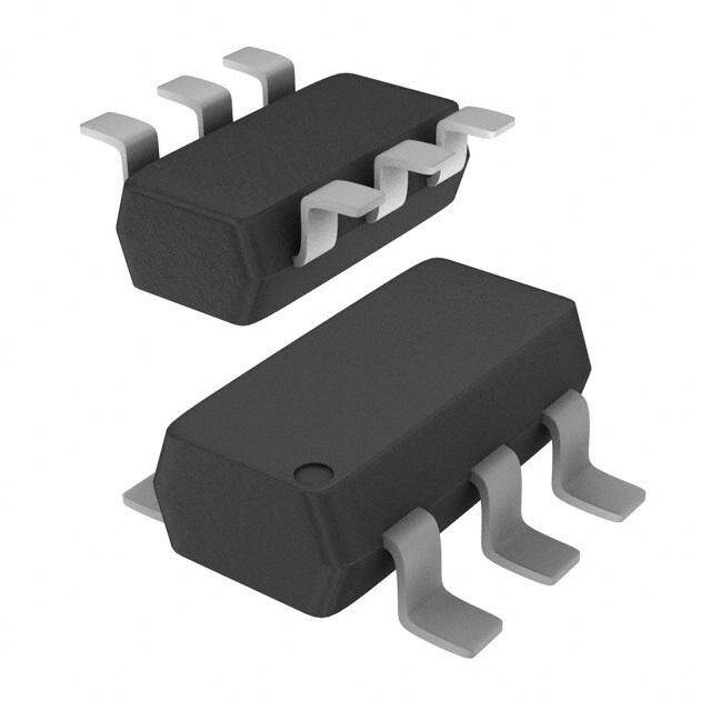
- 型号: 5.0SMDJ30A
- 制造商: Littelfuse
- 库位|库存: xxxx|xxxx
- 要求:
| 数量阶梯 | 香港交货 | 国内含税 |
| +xxxx | $xxxx | ¥xxxx |
查看当月历史价格
查看今年历史价格
5.0SMDJ30A产品简介:
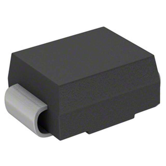
ICGOO电子元器件商城为您提供5.0SMDJ30A由Littelfuse设计生产,在icgoo商城现货销售,并且可以通过原厂、代理商等渠道进行代购。 5.0SMDJ30A价格参考。Littelfuse5.0SMDJ30A封装/规格:TVS - 二极管, 48.4V Clamp 103A Ipp Tvs Diode 表面贴装 DO-214AB(SMC)。您可以下载5.0SMDJ30A参考资料、Datasheet数据手册功能说明书,资料中有5.0SMDJ30A 详细功能的应用电路图电压和使用方法及教程。
| 参数 | 数值 |
| 产品目录 | |
| 描述 | TVS DIODE 30VWM 48.4VC SMDTVS 二极管 - 瞬态电压抑制器 TVS Diode SMC Suf MT |
| 产品分类 | |
| 品牌 | Littelfuse |
| 产品手册 | |
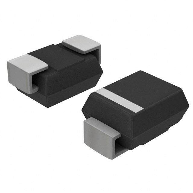
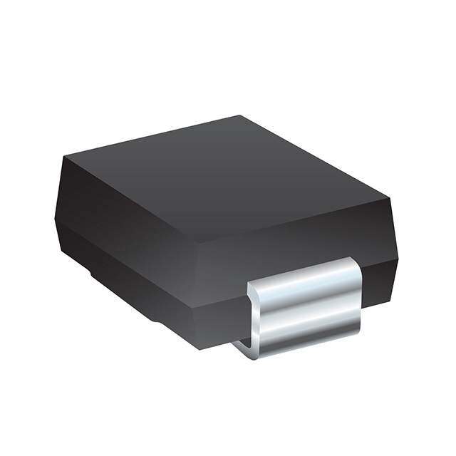
| 产品图片 |
|
| rohs | 符合RoHS不受无铅要求限制 / 符合限制有害物质指令(RoHS)规范要求 |
| 产品系列 | 二极管与整流器,TVS二极管,TVS 二极管 - 瞬态电压抑制器,Littelfuse 5.0SMDJ30A5.0SMDJ |
| 数据手册 | |
| 产品型号 | 5.0SMDJ30A |
| 不同频率时的电容 | - |
| 产品培训模块 | http://www.digikey.cn/PTM/IndividualPTM.page?site=cn&lang=zhs&ptm=22970 |
| 产品目录绘图 |
|
| 产品种类 | TVS 二极管 - 瞬态电压抑制器 |
| 供应商器件封装 | DO-214AB (SMCJ) |
| 其它名称 | 5.0SMDJ30A-ND |
| 击穿电压 | 33.3 V |
| 功率-峰值脉冲 | 5000W (5kW) |
| 包装 | 带卷 (TR) |
| 单向通道 | 1 |
| 双向通道 | - |
| 商标 | Littelfuse |
| 安装类型 | 表面贴装 |
| 安装风格 | SMD/SMT |
| 封装 | Reel |
| 封装/外壳 | DO-214AB,SMC |
| 封装/箱体 | DO-214AB |
| 尺寸 | 6.22 mm W x 7.11 mm L x 2.62 mm H |
| 峰值浪涌电流 | 103 A |
| 峰值脉冲功率耗散 | 5 kW |
| 工作温度 | -55°C ~ 150°C |
| 工作电压 | 30 V |
| 工厂包装数量 | 3000 |
| 应用 | 通用 |
| 最大工作温度 | + 150 C |
| 最小工作温度 | - 65 C |
| 极性 | Unidirectional |
| 标准包装 | 3,000 |
| 电压-击穿(最小值) | 33.3V |
| 电压-反向关态(典型值) | 30V |
| 电压-箝位(最大值)@Ipp | 48.4V |
| 电流-峰值脉冲(10/1000µs) | 103A |
| 电源线路保护 | 无 |
| 端接类型 | SMD/SMT |
| 类型 | 齐纳 |
| 系列 | 5.0SMDJ |
| 钳位电压 | 48.4 V |




- 商务部:美国ITC正式对集成电路等产品启动337调查
- 曝三星4nm工艺存在良率问题 高通将骁龙8 Gen1或转产台积电
- 太阳诱电将投资9.5亿元在常州建新厂生产MLCC 预计2023年完工
- 英特尔发布欧洲新工厂建设计划 深化IDM 2.0 战略
- 台积电先进制程称霸业界 有大客户加持明年业绩稳了
- 达到5530亿美元!SIA预计今年全球半导体销售额将创下新高
- 英特尔拟将自动驾驶子公司Mobileye上市 估值或超500亿美元
- 三星加码芯片和SET,合并消费电子和移动部门,撤换高东真等 CEO
- 三星电子宣布重大人事变动 还合并消费电子和移动部门
- 海关总署:前11个月进口集成电路产品价值2.52万亿元 增长14.8%

PDF Datasheet 数据手册内容提取
NT *RoHS VCEOARVMSIAPILOLINAASB LE Features NT MPLIA n RoHS compliant* and halogen free** O HS C n Surface mount SMC package Ro * n Standoff voltage: 5 to 170 volts n Peak Pulse Power: 5000 watts n Typical temperature coefficient: DVBR = 0.1 % x VBR @ 25 °C xD T REE D F LEA 5.0SMDJ Transient Voltage Suppressor Diode Series General Information PhBioogruhtraenbrs lpe oo cfwfoeemrsr m dTeurannnsicsitaiyet incoitnr cVsuo, ilctt aopgmroept eSuctuitnpiogpn ra ecnsodsm ovLprViER dEoADoReDHn SIiSFo oeORC NEdnOeSE eMtqAsPsRLu.IE AifpNoTmr* seunrtg me aannudf aEcStuDr eprrso atercet icohna allepnpglicinagti othnes ,s ienm ciocmonpdaucct tcohr ipin dpuasctkrayg teo DdeOv-e2l1o4pA inBc r(eSaMsCin)g ly size format. The Transient Voltage Suppressor series offers a choice of Working Peak Reverse Voltage from 5 V up to 170 V and Breakdown Voltage up to 209 V. Typical fast response times are less than 1.0 ps from 0 V to Breakdown Voltage. Bourns® Chip Diodes conform to JEDEC standards, are easy to handle with standard pick and place equipment and the flat configuration minimizes roll away. Electrical Characteristics (@ TA = 25 °C Unless Otherwise Noted) Parameter Symbol Value Unit Minimum Peak Pulse Power Dissipation (Tp = 1 ms) (Note 1,2) PPK 5000 Watts Peak Forward Surge Current 8.3 ms Single Half Sine Wave Superimposed on Rated Load IFSM 300 Amps (JEDEC Method) (Note 3,4) Steady State Power Dissipation @ TL = 50 °C PM(AV) 6.5 Watts M(Faoxr imUnuimdi rIencsttiaonntaal nUenoiutss OFnolryw)ard Voltage @ IPP = 100 A VF 5 Volts Operating Temperature Range TJ -55 to +150 °C Storage Temperature Range TSTG -55 to +150 °C 1. Non-repetitive current pulse, per Pulse Waveform graph and derated above TA = 25 °C per Pulse Derating Curve. 2. Thermal Resistance Junction to Lead. 3. 8.3 ms Single Sine Wave duty cycle = 4 pulses maximum per minute (unidirectional units only). 4. Mounted on 8.0 mm x 8.0 mm copper pad area to each terminal. How to Order 5.0SMDJ 12 CA - H Package Asia-Pacific: 5.0SMDJ = SMC/DO-214AB Tel: +886-2 2562-4117 Working Peak Reverse Voltage Email: asiacus@bourns.com 12 = 12 VRWM (Volts) Europe: Suffix A = 5 % Tolerance Unidirectional Device Tel: +36 88 520 390 CA = 5 % Tolerance Bidirectional Device Email: eurocus@bourns.com Reel The Americas: (Blank) = 13-inch Reel Tel: +1-951 781-5500 -H = 7-inch Reel Email: americus@bourns.com www.bourns.com * RoHS Directive 2015/863, Mar 31, 2015 and Annex. **Bourns considers a product to be “halogen free” if (a) the Bromine (Br) content is 900 ppm or less; (b) the Chlorine (Cl) content is 900 ppm or less; and (c) the total Bromine (Br) and Chlorine (Cl) content is 1500 ppm or less. Specifications are subject to change without notice. The device characteristics and parameters in this data sheet can and do vary in different applications and actual device performance may vary over time. Users should verify actual device performance in their specific applications.
5.0SMDJ Transient Voltage Suppressor Diode Series Electrical Characteristics (@ TA = 25 °C Unless Otherwise Noted) Maximum Maximum Reverse Peak Breakdown Voltage Reverse Clamping Unidirectional Device Bidirectional Device Standoff Pulse VBR (Volts) Voltage Leakage Voltage Current @ VRWM @ IPP Part Part Part Part Number Marking Number Marking Min. Max. @ IT (mA) VRWM (V) IR (μA) VC (V) IPP (A) 5.0SMDJ5.0A 5RDE 5.0SMDJ5.0CA 5DDE 6.40 7.00 10 5.0 1050 9.2 543.6 5.0SMDJ6.0A 5RDG 5.0SMDJ6.0CA 5DDG 6.67 7.37 10 6.0 1050 10.3 485.5 5.0SMDJ6.5A 5RDK 5.0SMDJ6.5CA 5DDK 7.22 7.98 10 6.5 750 11.2 446.5 5.0SMDJ7.0A 5PDM 5.0SMDJ7.0CA 5DDM 7.78 8.60 10 7.0 300 12.0 416.8 5.0SMDJ7.5A 5PDP 5.0SMDJ7.5CA 5DDP 8.33 9.21 1 7.5 150 12.9 387.7 5.0SMDJ8.0A 5PDR 5.0SMDJ8.0CA 5DDR 8.89 9.83 1 8.0 70 13.6 367.7 5.0SMDJ8.5A 5PDT 5.0SMDJ8.5CA 5DDT 9.44 10.40 1 8.5 30 14.4 347.3 5.0SMDJ9.0A 5PDV 5.0SMDJ9.0CA 5DDV 10.00 11.10 1 9.0 12 15.4 324.8 5.0SMDJ10A 5PDX 5.0SMDJ10CA 5DDX 11.10 12.30 1 10.0 6 17.0 294.2 5.0SMDJ11A 5PDZ 5.0SMDJ11CA 5DDZ 12.20 13.50 1 11.0 2 18.2 274.8 5.0SMDJ12A 5PEP 5.0SMDJ12CA 5BEP 13.30 14.70 1 12.0 2 19.9 252.0 5.0SMDJ13A 5PEQ 5.0SMDJ13CA 5BEQ 14.40 15.90 1 13.0 2 21.5 233.0 5.0SMDJ14A 5PER 5.0SMDJ14CA 5BER 15.60 17.20 1 14.0 2 23.2 216.0 5.0SMDJ15A 5PES 5.0SMDJ15CA 5BES 16.70 18.50 1 15.0 2 24.4 205.0 5.0SMDJ16A 5PET 5.0SMDJ16CA 5BET 17.80 19.70 1 16.0 2 26.0 193.0 5.0SMDJ17A 5PEU 5.0SMDJ17CA 5BEU 18.90 20.90 1 17.0 2 27.6 181.0 5.0SMDJ18A 5PEV 5.0SMDJ18CA 5BEV 20.00 22.10 1 18.0 2 29.2 172.0 5.0SMDJ20A 5PEW 5.0SMDJ20CA 5BEW 22.20 24.50 1 20.0 2 32.4 155.0 5.0SMDJ22A 5PEX 5.0SMDJ22CA 5BEX 24.40 26.90 1 22.0 2 35.5 141.0 5.0SMDJ24A 5PEZ 5.0SMDJ24CA 5BEZ 26.70 29.50 1 24.0 2 38.9 129.0 5.0SMDJ26A 5PFE 5.0SMDJ26CA 5BFE 28.90 31.90 1 26.0 2 42.1 119.0 5.0SMDJ28A 5PFG 5.0SMDJ28CA 5BFG 31.10 34.40 1 28.0 2 45.4 110.0 5.0SMDJ30A 5PFK 5.0SMDJ30CA 5BFK 33.30 36.80 1 30.0 2 48.4 103.0 5.0SMDJ33A 5PFM 5.0SMDJ33CA 5BFM 36.70 40.60 1 33.0 2 53.3 93.9 5.0SMDJ36A 5PFP 5.0SMDJ36CA 5BFP 40.00 44.20 1 36.0 2 58.1 86.1 5.0SMDJ40A 5PFR 5.0SMDJ40CA 5BFR 44.40 49.10 1 40.0 2 64.5 77.6 5.0SMDJ43A 5PFT 5.0SMDJ43CA 5BFT 47.80 52.80 1 43.0 2 69.4 72.1 5.0SMDJ45A 5PFV 5.0SMDJ45CA 5BFV 50.00 55.30 1 45.0 2 72.7 68.8 5.0SMDJ48A 5PFX 5.0SMDJ48CA 5BFX 53.30 58.90 1 48.0 2 77.4 64.7 5.0SMDJ51A 5PFZ 5.0SMDJ51CA 5BFZ 56.70 62.70 1 51.0 2 82.4 60.7 5.0SMDJ54A 5RGE 5.0SMDJ54CA 5BGE 60.00 66.30 1 54.0 2 87.1 57.5 5.0SMDJ58A 5PGG 5.0SMDJ58CA 5BGG 64.40 71.20 1 58.0 2 93.6 53.5 5.0SMDJ60A 5PGK 5.0SMDJ60CA 5BGK 66.70 73.70 1 60.0 2 96.8 51.7 5.0SMDJ64A 5PGM 5.0SMDJ64CA 5BGM 71.10 78.60 1 64.0 2 103.0 48.6 5.0SMDJ70A 5PGP 5.0SMDJ70CA 5BGP 77.80 86.00 1 70.0 2 113.0 44.3 5.0SMDJ75A 5PGR 5.0SMDJ75CA 5BGR 83.30 92.10 1 75.0 2 121.0 41.4 5.0SMDJ78A 5PGT 5.0SMDJ78CA 5BGT 86.70 95.80 1 78.0 2 126.0 39.7 5.0SMDJ85A 5PGV 5.0SMDJ85CA 5BGV 94.40 104.00 1 85.0 2 137.0 36.5 5.0SMDJ90A 5PGX 100.00 111.00 1 90.0 2 146.0 34.3 5.0SMDJ100A 5PGZ 111.00 123.00 1 100.0 2 162.0 30.9 5.0SMDJ110A 5PHE 122.00 135.00 1 110.0 2 177.0 28.3 5.0SMDJ120A 5PHG 133.00 147.00 1 120.0 2 193.0 26.0 5.0SMDJ130A 5PHK 144.00 159.00 1 130.0 2 209.0 24.0 5.0SMDJ150A 5PHM 167.00 185.00 1 150.0 2 243.0 20.6 5.0SMDJ160A 5PHP 178.00 197.00 1 160.0 2 259.0 19.3 5.0SMDJ170A 5PHR 189.00 209.00 1 170.0 2 275.0 18.2 Specifications are subject to change without notice. The device characteristics and parameters in this data sheet can and do vary in different applications and actual device performance may vary over time. Users should verify actual device performance in their specific applications.
5.0SMDJ Transient Voltage Suppressor Diode Series A Product Dimensions Recommended Footprint A A B C A B B C B C CATHODE BAND (UNIDIRECTIONAL DEVICES ONLY) Dimension SMC (DO-214AB) G C 4.69 A (Max.) CATHODE BAND (0.185) (UNIDIRECTIONAL DEVICES ONLY) 3.07 G B (Min.) (0.121) 1.53 H F D C (Min.) (0.060) E MM H F D D IMENSIONS: (INCHES) E MM DIMENSIONS: (INCHES) Physical Specifications Dimension SMMCM (DO-214AB) DIMENSIONS: (INC6HE.S6)0 - 7.11 Encapsulation .............................Molded plastic per UL Class 94V-0 A Polarity.......................Cathode band indicates unidirectional device (0.260 - 0.280) No cathode band indicates bidirectional device 5.59 - 6.22 B (0.220 - 0.245) 2.90 - 3.20 C Environmental Specifications (0.114 - 0.126) 0.15 - 0.31 Moisture Sensitivity Level ................................................................1 D (0.006 - 0.112) ESD Classification (HBM).............................................................3B 7.75 - 8.13 E (0.305 - 0.320) 0.05 - 0.20 F (0.002 - 0.008) 2.01 - 2.62 G (0.080 - 0.103) 0.76 - 1.52 H (0.030 - 0.060) MM DIMENSIONS: (INCHES) Specifications are subject to change without notice. The device characteristics and parameters in this data sheet can and do vary in different applications and actual device performance may vary over time. Users should verify actual device performance in their specific applications.
5.0SMDJ Transient Voltage Suppressor Diode Series Rating & Characteristic Curves Pulse Derating Curve Maximum Non-Repetitive Surge Current 100 300 s) Peak Pulse Derating in Percent ofPeak Power or Current 752505 10 x 1000 Wbya vRe.fEo.rAm. as Defined Peak Forward Surge Current (Amp22115050500000 310000 AA aatt 18 0c yccylceles 0 0 0 25 50 75 100 125 150 175 200 1 2 5 10 20 50 100 Junction Temperature (°C) Number of Cycles at 60 Hz Pulse Waveform Typical Junction Capacitance 100000 TR=10 µs Peak value (IRSM) 100 Bidirectional v=0v I, Peak Pulse Current (%)P 50 TA=T2P5 °C Half value=IR2SMdiwes1ca hd0asPeey rudxfsei len s 1ttfeeo0hind 0ew5e 0adp0ids e wb %tathayhk v a( oRceTtf u.f PpEoIrP)o.rrA meSin.nMtt . C - Junction Capacitance (pF)J11010001000000 TJ = 25 °C Unid@ire VctRional Bidi@re cVtiRonal Unidirectional v=0v f = 1.0 MHz Vsig = 50 mVp-p 0 1 0 1.0 2.0 3.0 4.0 1 10 100 1000 T, Time (ms) VBR - Reverse Breakdown Voltage (V) Pulse Rating Curve Steady State Power Derating Curve 1000 6.5 W) TA = 25 °C W) 6.0 er (k 100 ation ( 55..05 w p Pulse Po 10 Power Dissi 443...055 eak State 32..05 - P ady 2.0 PPPM 1 8.0 x 8.0 mm SteM(AV) 11..05 60 Hz Resistive or (0.31 x 0.31 in.) P 0.5 Inductive Load Copper Pad Areas 0.1 0.0 0.1 µs 1.0 µs 10 µs 100 µs 1.0 ms 10 ms 0 25 50 75 100 125 150 175 200 TL, Lead Temperature (°C) td - Pulse Width (sec.) Specifications are subject to change without notice. The device characteristics and parameters in this data sheet can and do vary in different applications and actual device performance may vary over time. Users should verify actual device performance in their specific applications.
C5.D0DSFMND5J- 0T5ra0n4sNie -n tT VVoSl/tSagteee Sriunpgp rDeisosdoer DAirordaey Series Packaging Information The product will be dispensed in tape and reel format (see diagram below). P 0 P1 E T d Index Hole 120 ° F D2 W B D1 D P A C Trailer Device Leader ....... ....... ....... ....... W1 End ....... ....... ....... ....... Start MM DIMENSIONS: (INCHES) 10 pitches (min.) 10 pitches (min.) Devices are packed in accordance with EIA standard Direction of Feed EIA-481-D and specifications shown here. Item Symbol SMC (DO-214AB) 7-Inch Reel 13-Inch Reel 6.0 ± 0.20 Carrier Width A (0.236 ± 0.079) 8.3 ± 0.20 Carrier Length B (0.327 ± 0.008) 2.5 ± 0.20 Carrier Depth C (0.098 ± 0.008) 1.50 ± 0.10 Sprocket Hole d (0.059 ± 0.004) 178 330 Reel Outside Diameter D (7.008) (12.992) 50.0 Reel Inner Diameter D1 (1.969) MIN. 13.0 +0.50/-0.20 Feed Hole Diameter D2 (0.512 +0.020/-0.008) 1.75 ± 0.10 Sprocket Hole Position E (0.069 ± 0.004) 7.50 ± 0.10 Punch Hole Position F (0.295 ± 0.004) 8.00 ± 0.10 Punch Hole Pitch P (0.315 ± 0.004) 4.00 ± 0.10 Sprocket Hole Pitch P0 (0.157 ± 0.004) 2.00 ± 0.10 Embossment Center P1 (0.079 ± 0.004) 0.30± 0.10 Overall Tape Thickness T (0.012 ± 0.004) 16.00 ± 0.30 Tape Width W (0.630 ± 0.012) 22.4 Reel Width W1 (0.882) MAX. Quantity per Reel -- 500 3,000 05/18 Specifications are subject to change without notice. The device characteristics and parameters in this data sheet can and do vary in different applications and actual device performance may vary over time. Users should verify actual device performance in their specific applications.
 Datasheet下载


