ICGOO在线商城 > 射频/IF 和 RFID > RF 收发器模块 > 450-0067
 Datasheet下载
- 型号: 450-0067
- 制造商: LS Research
- 库位|库存: xxxx|xxxx
- 要求:
| 数量阶梯 | 香港交货 | 国内含税 |
| +xxxx | $xxxx | ¥xxxx |
查看当月历史价格
查看今年历史价格
450-0067产品简介:
ICGOO电子元器件商城为您提供450-0067由LS Research设计生产,在icgoo商城现货销售,并且可以通过原厂、代理商等渠道进行代购。 450-0067价格参考¥询价-¥询价。LS Research450-0067封装/规格:RF 收发器模块, WiFi 802.11b/g Transceiver Module 2.4GHz 不包括 表面贴装。您可以下载450-0067参考资料、Datasheet数据手册功能说明书,资料中有450-0067 详细功能的应用电路图电压和使用方法及教程。
| 参数 | 数值 |
| 产品目录 | |
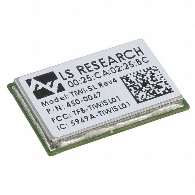
| 描述 | MODULE TIWI-SL 802.11WiFi/802.11模块 TiWi-SL CC3000 Module |
| 产品分类 | RF 收发器射频/无线模块 |
| 品牌 | LS Research |
| 产品手册 | |
| 产品图片 |
|
| rohs | 符合RoHS无铅 / 符合限制有害物质指令(RoHS)规范要求 |
| 产品系列 | WiFi/802.11模块,LS Research 450-0067- |
| 数据手册 | |
| 产品型号 | 450-0067 |
| PCN设计/规格 | |
| RoHS指令信息 | |
| 产品种类 | WiFi/802.11模块 |
| 传输供电电流 | 269 mA |
| 传输功率—最大值 | 20 dBm |
| 其它名称 | 4500067 |
| 功率-输出 | 20dBm |
| 包装 | 托盘 |
| 商标 | LS Research |
| 天线连接器 | PCB,表面贴装 |
| 天线连接器类型 | Chip, PCB |
| 存储容量 | - |
| 安全 | WEP, WPA, WPA2 |
| 封装/外壳 | 40-SMD 模块 |
| 尺寸 | 21 mm x 14 mm x 2.3 mm |
| 工作温度 | -30°C ~ 75°C |
| 工作电源电压 | 3.3 V |
| 工厂包装数量 | 100 |
| 应用 | WLAN |
| 接口类型 | SPI |
| 接收供电电流 | 92 mA |
| 支持协议 | 802.11 b/g |
| 数据接口 | PCB,表面贴装 |
| 数据速率 | 11 Mb/s, 54 Mb/s |
| 数据速率(最大值) | 54Mbps |
| 最大工作温度 | + 85 C |
| 最小工作温度 | - 40 C |
| 标准包装 | 100 |
| 灵敏度 | -85dBm |
| 电压-电源 | 2.9 V ~ 3.6 V |
| 电流-传输 | 276mA |
| 电流-接收 | 276mA |
| 调制或协议 | 802.11b/g |
| 调制技术 | DSSS, OFDM |
| 频带 | 2.4 GHz |
| 频率 | 2.4GHz |


- 商务部:美国ITC正式对集成电路等产品启动337调查
- 曝三星4nm工艺存在良率问题 高通将骁龙8 Gen1或转产台积电
- 太阳诱电将投资9.5亿元在常州建新厂生产MLCC 预计2023年完工
- 英特尔发布欧洲新工厂建设计划 深化IDM 2.0 战略
- 台积电先进制程称霸业界 有大客户加持明年业绩稳了
- 达到5530亿美元!SIA预计今年全球半导体销售额将创下新高
- 英特尔拟将自动驾驶子公司Mobileye上市 估值或超500亿美元
- 三星加码芯片和SET,合并消费电子和移动部门,撤换高东真等 CEO
- 三星电子宣布重大人事变动 还合并消费电子和移动部门
- 海关总署:前11个月进口集成电路产品价值2.52万亿元 增长14.8%


PDF Datasheet 数据手册内容提取
TiWi-SL MODULE DATASHEET Integrated 802.11 b/g WLAN Module FEATURES DESCRIPTION IEEE 802.11 b/g compliant. The TiWi-SL is a high performance 2.4 GHz WLAN module that contains an IP networking Typical WLAN Transmit Power: stack in a pre-certified footprint that simplifies o +20.0 dBm, 1 Mbps, CCK (b) the process of implementing internet o +16.9 dBm, 54 Mbps, OFDM (g) connectivity. Typical WLAN Sensitivity: o - 85 dBm, 8% PER,11 Mbps o -75 dBm, 10% PER, 54 Mbps Miniature footprint: 14 mm x 21 mm Low height profile: 2.3 mm Operating Voltage: 2.9V to 3.6V Operating temperature: -40 to +85o C Embedded network stack Wireless Security WEP, WPA Personal, WPA2 Personal The module includes the necessary PHY, MAC, and network layers to support WLAN Terminal for PCB/Chip antenna feeds applications through a simple SPI connection to Compact design based on Texas host microcontrollers or other embedded Instruments CC3000 transceiver processors. SPI host interface Simple integration with microcontrollers and Need to get to market quickly? Not an expert in microprocessors 802.11. Need a custom antenna? Would you Worldwide acceptance: FCC (USA), IC like to own the design? Would you like a (Canada), and CE (Europe) custom design? Not quite sure what you need? Do you need help with your host board? LS Modular certification allows reuse of LSR FCC ID and ETSI certification without Research Design Services will be happy to repeating the expensive testing on your end develop custom hardware or software, or assist product with integrating the design. Contact us at RoHS compliant sales@lsr.com or call us at 262-375-4400. Streamlined development with LSR design Home automation services Home Network aggregators Remote appliance diagnostics/support APPLICATIONS Home security Remote storage devices Thermostats, appliances, HVAC controller, Home network appliance and remote displays, Smart Energy Cameras and video surveillance Home entertainment control Fitness Sensor Networks Cable replacement for medical and personal healthcare Medical Home Monitoring Toys The information in this document is subject to change without notice. 330-0085-R3.0 Copyright © 2011-2012 LS Research, LLC Page 1 of 39
TiWi-SL MODULE DATASHEET ORDERING INFORMATION Order Number Description 450-0067 TiWi-SL Module (Tray, SPQ = 50) 450-0067R TiWi-SL Module (Tape and Reel, SPQ = 1000) 450-0089 TiWi-SL EM Board with Chip Antenna Table 1 Orderable TiWi-SL Part Numbers MODULE ACCESSORIES Order Number Description 2.4 GHz Dipole Antenna with Reverse 001-0001 Polarity SMA Connector U.FL to Reverse Polarity SMA Bulkhead 080-0001 Cable 105mm Table 2 Module Accessories APPLICABLE DOCUMENTS TiWi-SL EM Board User Guide (330-0086) TiWi-SL Antenna Design Guide (330-0092) The information in this document is subject to change without notice. 330-0085-R3.0 Copyright © 2011-2012 LS Research, LLC Page 2 of 39
TiWi-SL MODULE DATASHEET BLOCK DIAGRAM Figure 1 TiWi-SL Module Block Diagram – Top Level The information in this document is subject to change without notice. 330-0085-R3.0 Copyright © 2011-2012 LS Research, LLC Page 3 of 39
TiWi-SL MODULE DATASHEET FUNCTIONAL BLOCK FEATURES WLAN Features IEEE802.11b/g compliant WLAN MAC Baseband Processor and RF transceiver IEEE Std 802.11d,i PICS compliant Supports serial debug interface Supports Serial Peripheral Interface (SPI) Host Interface Media Access Controller (MAC) o Embedded ARM™ Central Processing Unit (CPU) o Hardware-Based Encryption/Decryption Using 64-, 128-Bit WEP, TKIP or AES Keys, o Supports requirements for Wireless Fidelity (Wi-Fi) Protected Access (WPA and WPA2.0) and IEEE o Std 802.11i [Includes Hardware-Accelerated Advanced-Encryption Standard (AES)] Baseband Processor 2.4GHz Radio o Digital Radio Processor (DRP) implementation o Internal LNA o Supports : IEEE Std 802.11b, 802.11g, 802.11b/g Network Stack Supported Protocols Transport layer: o TCP o UDP Network layer: o IPv4 o Ping o DHCP o DNS Client Link layer: o ARP Wireless Security System Features Supported modes: o Open (no security) o WEP o WPA-personal o WPA2-personal Supported encryption types: o WEP o TKIP o AES o Open The information in this document is subject to change without notice. 330-0085-R3.0 Copyright © 2011-2012 LS Research, LLC Page 4 of 39
TiWi-SL MODULE DATASHEET TABLE OF CONTENTS FEATURES .......................................................................................................................... 1 APPLICATIONS ................................................................................................................... 1 DESCRIPTION ..................................................................................................................... 1 ORDERING INFORMATION ................................................................................................ 2 MODULE ACCESSORIES ................................................................................................... 2 APPLICABLE DOCUMENTS ............................................................................................... 2 BLOCK DIAGRAM ............................................................................................................... 3 FUNCTIONAL BLOCK FEATURES .................................................................................... 4 WLAN Features ........................................................................................................................................... 4 Network Stack Supported Protocols ......................................................................................................... 4 Wireless Security System Features .......................................................................................................... 4 PIN DESCRIPTIONS ............................................................................................................ 8 ELECTRICAL SPECIFICATIONS ...................................................................................... 10 Absolute Maximum Ratings ..................................................................................................................... 10 Recommended Operating Conditions .................................................................................................... 10 General Characteristics ............................................................................................................................ 11 TCP and UDP Throughput ........................................................................................................................ 12 Power Consumption ................................................................................................................................. 13 RF Characteristics .................................................................................................................................... 14 SPI HOST CONTROLLER INTERFACE ............................................................................ 20 Overview .................................................................................................................................................... 20 SPI Interface Description .......................................................................................................................... 20 SPI Line Description ................................................................................................................................. 20 SPI Timing .................................................................................................................................................. 21 DEVICE POWER-UP AND ENABLE ................................................................................. 22 DEVICE POWER-DOWN ................................................................................................... 23 SOLDERING RECOMMENDATIONS ................................................................................ 24 Recommended Reflow Profile for Lead Free Solder ............................................................................. 24 CLEANING ......................................................................................................................... 25 The information in this document is subject to change without notice. 330-0085-R3.0 Copyright © 2011-2012 LS Research, LLC Page 5 of 39
TiWi-SL MODULE DATASHEET OPTICAL INSPECTION ..................................................................................................... 25 REWORK ........................................................................................................................... 25 SHIPPING, HANDLING, AND STORAGE ......................................................................... 25 Shipping ..................................................................................................................................................... 25 Handling ..................................................................................................................................................... 25 Moisture Sensitivity Level (MSL) ............................................................................................................. 25 Storage ....................................................................................................................................................... 25 Repeating Reflow Soldering .................................................................................................................... 26 AGENCY CERTIFICATIONS ............................................................................................. 27 AGENCY STATEMENTS ................................................................................................... 27 Federal Communication Commission Interference Statement ............................................................ 27 Industry Canada Statements.................................................................................................................... 28 OEM RESPONSIBILITIES TO COMPLY WITH FCC AND INDUSTRY CANADA REGULATIONS ....................................................................................................... 29 OEM LABELING REQUIREMENTS FOR END-PRODUCT .............................................. 30 OEM END PRODUCT USER MANUAL STATEMENTS.................................................... 31 EUROPE ............................................................................................................................ 32 CE Notice ................................................................................................................................................... 32 Declaration of Conformity (DOC) ............................................................................................................ 32 MECHANICAL DATA......................................................................................................... 33 PCB FOOTPRINT .............................................................................................................. 34 TRAY PACKAGING (MM) .................................................................................................. 35 TAPE AND REEL PACKAGING ........................................................................................ 36 REFERENCE SCHEMATIC ............................................................................................... 37 DEVICE MARKINGS .......................................................................................................... 38 Rev 1 Devices ............................................................................................................................................ 38 Rev 2 and Rev 3 Devices .......................................................................................................................... 38 CONTACTING LS RESEARCH ......................................................................................... 39 The information in this document is subject to change without notice. 330-0085-R3.0 Copyright © 2011-2012 LS Research, LLC Page 6 of 39
TiWi-SL MODULE DATASHEET TIWI-SL MODULE FOOTPRINT AND PIN DEFINITIONS To apply the TiWi-SL module, it is important to use the module pins in your application as they are designated below, and in the corresponding pin definition table found on pages 8 and 9. Not all the pins on the TiWi-SL module may be used, as some are reserved. Figure 2 TiWi-SL Pinout The information in this document is subject to change without notice. 330-0085-R3.0 Copyright © 2011-2012 LS Research, LLC Page 7 of 39
TiWi-SL MODULE DATASHEET PIN DESCRIPTIONS Module I/O Buffer Logic Name Description Pin Type Type Level 1 GND GND - - GROUND 2 NC - - - NO CONNECT (DO NOT CONNECT) 3 NC - - - NO CONNECT (DO NOT CONNECT) 4 NC - - - NO CONNECT (DO NOT CONNECT) MODE1 (SHORT TO MODE2 FOR NORMAL USE, SHORT 5 MODE1 DI - - TO GROUND FOR TEST USE) 6 NC - - - NO CONNECT (DO NOT CONNECT) 7 UART_TX (1) DO - 1.8 VDC TEST UART TX (1.8V LOGIC) MODE2 (SHORT TO MODE1 FOR NORMAL USE, LEAVE 8 MODE2 DI - - OPEN FOR TEST USE) 9 UART_RX (1) DI - 1.8 VDC TEST UART RX (1.8V LOGIC) 10 NC - - - NO CONNECT (DO NOT CONNECT) 11 GND GND - - GROUND 12 GND GND - - GROUND 13 PWR_EN DI - VCC MODULE POWER ENABLE 14 GND GND - - GROUND 15 VCC PI - - POWER TO MODULE (2.9-3.6 VDC) 16 GND GND - - GROUND 17 GND GND - - GROUND 18 SPI_DI DI - VCC HOST INTERFACE SPI DATA IN 19 SPI_CLK DI - VCC HOST INTERFACE SPI CLOCK 20 /SPI_CS DI - VCC HOST INTERFACE SPI CHIP SELECT (ACTIVE LOW) 21 SPI_DO DO 10mA VCC HOST INTERFACE SPI DATA OUT 22 /SPI_IRQ DO 10mA VCC HOST INTERFACE SPI INTERRUPT (ACTIVE LOW) 23 GND GND - - GROUND 24 GND GND - - GROUND 25 NC - - - NO CONNECT (DO NOT CONNECT) 26 NC - - - NO CONNECT (DO NOT CONNECT) 27 GND GND - - GROUND 28 SDA_EE (2) DIO - 1.8 VDC I2C DATA LINE FROM EEPROM (1.8V LOGIC) I2C DATA LINE FROM CC3000, PULLED UP 29 SDA_CC (2) DIO 4mA 1.8 VDC INTERNALLY (1.8V LOGIC) 30 SCL_EE (3) DI - 1.8 VDC I2C CLOCK LINE FROM EEPROM (1.8V LOGIC) The information in this document is subject to change without notice. 330-0085-R3.0 Copyright © 2011-2012 LS Research, LLC Page 8 of 39
TiWi-SL MODULE DATASHEET Module I/O Buffer Logic Name Description Pin Type Type Level I2C CLOCK LINE FROM CC3000, PULLED UP 31 SCL_CC (3) DO 4mA 1.8 VDC INTERNALLY (1.8V LOGIC) 32 GND GND - - GROUND 33 GND GND - - GROUND 34 GND GND - - GROUND 35 GND GND - - GROUND 36 ANT (4) RF - - ANTENNA, 50 OHMS 37 GND GND - - GROUND 38 GND GND - - GROUND 39 GND GND - - GROUND 40 GND GND - - GROUND 41 GND GND - - GROUND 42 GND GND - - GROUND 43 GND GND - - GROUND 44 GND GND - - GROUND (1) These signals are test UART signals which are 1.8v logic, and they should be left unconnected for normal operation. (2) The I2C data signals from the CC3000 and EEPROM must be connected together for normal operation. (3) The I2C clock signals from the CC3000 and EEPROM must be connected together for normal operation. (4) The antenna terminal presents a DC short circuit to ground. PI = Power Input DI = Digital Input DO = Digital Output DIO = Bi-directional Digital Port RF = Bi-directional RF Port GND=Ground Table 3 TiWi-SL Module Pin Descriptions The information in this document is subject to change without notice. 330-0085-R3.0 Copyright © 2011-2012 LS Research, LLC Page 9 of 39
TiWi-SL MODULE DATASHEET ELECTRICAL SPECIFICATIONS Absolute Maximum Ratings Parameter Min Max Unit Power supply voltage (VCC) -0.5 +3.8 V Voltage on digital pins (1) -0.5 VCC + 0.5 V Voltage on EEPROM and UART test pins (2) -0.5 2.1 V RF input power, antenna port +10 dBm Operating temperature -40 +85 ºC Storage temperature -55 +125 ºC (1) This includes the SPI signals and the PWR_EN signal. (2) These signals are not intended for general purpose use. Table 4 Absolute Maximum Ratings Recommended Operating Conditions Parameter Min Typical Max Unit VCC 2.9 3.3 3.6 V Voltage on digital pins (1) 0 3.3 VCC V Voltage on EEPROM and UART test pins (2) 0 1.8 V Ambient temperature range (3) -30 25 75 ºC (1) Applies to SPI signals. (2) These signals are not intended for general purpose use. (3) The device can be reliably operated for 5000 active hours cumulative at T of 85C. ambient Table 5 Recommended Operating Conditions The information in this document is subject to change without notice. 330-0085-R3.0 Copyright © 2011-2012 LS Research, LLC Page 10 of 39
TiWi-SL MODULE DATASHEET General Characteristics DC Characteristics – UART/EEPROM I/O Parameter Test Conditions Min Typical Max Unit Logic input low, V 0 - 0.63 V IL Logic input high, V 1.7 - 1.8 V IH Logic output low, V 8mA 0 - 0.45 V OL Logic output high, V 8mA 1.4 - 1.8 V OH Table 6 DC Characteristics General Purpose I/O DC Characteristics – General Purpose I/O Parameter Test Conditions Min Typical Max Unit Logic input low, V 0 - 0.8 V IL Logic input high, V 2.0 - VCC V IH Logic output low, V 12mA 0 - 0.8 V OL Logic output high, V 12mA 2.3 - VCC V OH Applies to the SPI signals and the PWR_EN signal. Table 7 DC Characteristics General Purpose I/O RF Characteristics Parameter Min Typical Max Unit RF frequency range 2412 2472 MHz 802.11 b/g RF data rate 1 54 Mbps rates supported Table 8 RF Characteristics The information in this document is subject to change without notice. 330-0085-R3.0 Copyright © 2011-2012 LS Research, LLC Page 11 of 39
TiWi-SL MODULE DATASHEET TCP and UDP Throughput Traffic Type Privacy Throughput (Mbps) UDP Tx Open 6.9 UDP Rx Open 5.5 TCP Tx Open 3.5 TCP Rx Open 2.6 UDP Tx WEP128 6.6 UDP Rx WEP128 5.5 TCP Tx WEP128 3.2 TCP Rx WEP128 2.5 UDP Tx WPAv1 6.5 UDP Rx WPAv1 5.5 TCP Tx WPAv1 3.3 TCP Rx WPAv1 2.4 UDP Tx WPAv2 6.8 UDP Rx WPAv2 5.5 TCP Tx WPAv2 3.3 TCP Rx WPAv2 2.5 Table 9 TCP and UDP Throughput The information in this document is subject to change without notice. 330-0085-R3.0 Copyright © 2011-2012 LS Research, LLC Page 12 of 39
TiWi-SL MODULE DATASHEET Power Consumption Parameter Test Conditions Min Typical Max Unit 2437 MHz, VCC = 3.3V, T = +25°C amb DSSS (b) TX Current Po = 19 dBm, 1 Mbps BPSK - 269 - mA L = 1200 bytes, t (idle) = 40 uS delay 2437 MHz, VCC = 3.3V, T = +25°C amb DSSS (b) TX Current Po = 19 dBm, 11 Mbps CCK - 269 - mA L = 1200 bytes, t (idle) = 40 uS delay 2437 MHz, VCC = 3.3V, T = +25°C amb OFDM (g) TX Current Po = 17 dBm, 18 Mbps QPSK - 223 - mA L = 1200 bytes, t (idle) = 4 uS delay 2437 MHz, VCC = 3.3V, T = +25°C amb OFDM (g) TX Current Po = 15 dBm, 54 Mbps 64-QAM - 187 - mA L = 1200 bytes, t (idle) = 4 uS delay DSSS (b) RX Current - 92 - mA OFDM (g) RX Current - 92 - mA Power Down Mode [1] - <1 - uA [1] Total Current from VCC when PWR_EN is low and VCC is present. Table 10 WLAN Power Consumption The information in this document is subject to change without notice. 330-0085-R3.0 Copyright © 2011-2012 LS Research, LLC Page 13 of 39
TiWi-SL MODULE DATASHEET RF Characteristics WLAN Transmitter Characteristics (TA = +25°C, VCC = 3.3 V) Parameter Test Conditions Min Typ Max Unit 1 Mbps BPSK 802.11(b) Mask Compliance 1 Mbps DSSS (b) TX Output Power - 20.2 - dBm 35% EVM RMS power over TX packet 2 Mbps QPSK 802.11(b) Mask Compliance 2 Mbps DSSS (b) TX Output Power - 20.2 - dBm 35% EVM RMS power over TX packet 11 Mbps CCK 802.11(b) Mask Compliance 11 Mbps DSSS (b) TX Output Power - 20.0 - dBm 35% EVM RMS power over TX packet 6 Mbps BPSK 802.11(g) Mask Compliance 6 Mbps OFDM (g) TX Output Power - 18.7 - dBm -5 dB EVM RMS power over TX packet 9 Mbps BPSK 802.11(g) Mask Compliance 9 Mbps OFDM (g) TX Output Power - 18.7 - dBm -8 dB EVM RMS power over TX packet 18 Mbps QPSK 802.11(g) Mask Compliance 18 Mbps OFDM (g) TX Output Power - 18.7 - dBm -13 dB EVM RMS power over TX packet 36 Mbps 16-QAM 802.11(g) Mask Compliance 36 Mbps OFDM (g) TX Output Power - 17.4 - dBm -19 dB EVM RMS power over TX packet 54 Mbps 64-QAM 802.11(g) Mask Compliance 54 Mbps OFDM (g) TX Output Power - 16.9 - dBm -25 dB EVM RMS power over TX packet Table 11 WLAN Transmitter RF Characteristics The information in this document is subject to change without notice. 330-0085-R3.0 Copyright © 2011-2012 LS Research, LLC Page 14 of 39
TiWi-SL MODULE DATASHEET WLAN Transmitter Characteristics (TA = +85°C, VCC = 3.3 V) Parameter Test Conditions Min Typ Max Unit 1 Mbps BPSK 802.11(b) Mask Compliance 1 Mbps DSSS (b) TX Output Power - 20.0 - dBm 35% EVM RMS power over TX packet 2 Mbps QPSK 802.11(b) Mask Compliance 2 Mbps DSSS (b) TX Output Power - 20.0 - dBm 35% EVM RMS power over TX packet 11 Mbps CCK 802.11(b) Mask Compliance 11 Mbps DSSS (b) TX Output Power - 19.9 - dBm 35% EVM RMS power over TX packet 6 Mbps BPSK 802.11(g) Mask Compliance 6 Mbps OFDM (g) TX Output Power - 18.4 - dBm -5 dB EVM RMS power over TX packet 9 Mbps BPSK 802.11(g) Mask Compliance 9 Mbps OFDM (g) TX Output Power - 18.4 - dBm -8 dB EVM RMS power over TX packet 18 Mbps QPSK 802.11(g) Mask Compliance 18 Mbps OFDM (g) TX Output Power - 18.4 - dBm -13 dB EVM RMS power over TX packet 36 Mbps 16-QAM 802.11(g) Mask Compliance 36 Mbps OFDM (g) TX Output Power - 17.1 - dBm -19 dB EVM RMS power over TX packet 54 Mbps 64-QAM 802.11(g) Mask Compliance 54 Mbps OFDM (g) TX Output Power - 16.7 - dBm -25 dB EVM RMS power over TX packet Table 12 WLAN Transmitter RF Characteristics The information in this document is subject to change without notice. 330-0085-R3.0 Copyright © 2011-2012 LS Research, LLC Page 15 of 39
TiWi-SL MODULE DATASHEET WLAN Transmitter Characteristics (TA = -40°C, VCC = 3.3 V) Parameter Test Conditions Min Typ Max Unit 1 Mbps BPSK 802.11(b) Mask Compliance 1 Mbps DSSS (b) TX Output Power - 19.8 - dBm 35% EVM RMS power over TX packet 2 Mbps QPSK 802.11(b) Mask Compliance 2 Mbps DSSS (b) TX Output Power - 19.8 - dBm 35% EVM RMS power over TX packet 11 Mbps CCK 802.11(b) Mask Compliance 11 Mbps DSSS (b) TX Output Power - 19.5 - dBm 35% EVM RMS power over TX packet 6 Mbps BPSK 802.11(g) Mask Compliance 6 Mbps OFDM (g) TX Output Power - 18.7 - dBm -5 dB EVM RMS power over TX packet 9 Mbps BPSK 802.11(g) Mask Compliance 9 Mbps OFDM (g) TX Output Power - 18.7 - dBm -8 dB EVM RMS power over TX packet 18 Mbps QPSK 802.11(g) Mask Compliance 18 Mbps OFDM (g) TX Output Power - 18.7 - dBm -13 dB EVM RMS power over TX packet 36 Mbps 16-QAM 802.11(g) Mask Compliance 36 Mbps OFDM (g) TX Output Power - 17.5 - dBm -19 dB EVM RMS power over TX packet 54 Mbps 64-QAM 802.11(g) Mask Compliance 54 Mbps OFDM (g) TX Output Power - 17.0 - dBm -25 dB EVM RMS power over TX packet Table 13 WLAN Transmitter RF Characteristics The information in this document is subject to change without notice. 330-0085-R3.0 Copyright © 2011-2012 LS Research, LLC Page 16 of 39
TiWi-SL MODULE DATASHEET WLAN Receiver Characteristics (TA = +25°C, VCC = 3.3V) [1] Parameter Test Conditions Min Typ Max Unit 1 Mbps DSSS (b) RX Sensitivity 8% PER - -98.4 - dBm 2 Mbps DSSS (b) RX Sensitivity 8% PER - -95.0 - dBm 11 Mbps DSSS (b) RX Sensitivity 8% PER - -88.3 - dBm 6 Mbps OFDM (g) RX Sensitivity 10% PER - -91.6 - dBm 9 Mbps OFDM (g) RX Sensitivity 10% PER - -90.8 - dBm 18 Mbps OFDM (g) RX Sensitivity 10% PER - -88.0 - dBm 36 Mbps OFDM (g) RX Sensitivity 10% PER - -81.3 - dBm 54 Mbps OFDM (g) RX Sensitivity 10% PER - -75.3 - dBm 1 Mbps DSSS (b) RX Overload Level 8% PER -10 - - dBm 2 Mbps DSSS (b) RX Overload Level 8% PER -10 - - dBm 11 Mbps DSSS (b) RX Overload Level 8% PER -10 - - dBm 9 Mbps OFDM (g) RX Overload Level 10% PER -17 - - dBm 18 Mbps OFDM (g) RX Overload Level 10% PER -17 - - dBm 36 Mbps OFDM (g) RX Overload Level 10% PER -17 - - dBm 54 Mbps OFDM (g) RX Overload Level 10% PER -17 - - dBm [1] Up to 2 dB degradation at Channel 13 for 11g modes and up to 2 dB degradation at Channel 14 for 11b/g modes. Table 14 WLAN Receiver RF Characteristics The information in this document is subject to change without notice. 330-0085-R3.0 Copyright © 2011-2012 LS Research, LLC Page 17 of 39
TiWi-SL MODULE DATASHEET WLAN Receiver Characteristics (TA = +85°C, VCC = 3.3V) [1] Parameter Test Conditions Min Typ Max Unit 1 Mbps DSSS (b) RX Sensitivity 8% PER - -97.0 - dBm 2 Mbps DSSS (b) RX Sensitivity 8% PER - -93.7 - dBm 11 Mbps DSSS (b) RX Sensitivity 8% PER - -88.0 - dBm 6 Mbps OFDM (g) RX Sensitivity 10% PER - -90.5 - dBm 9 Mbps OFDM (g) RX Sensitivity 10% PER - -89.5 - dBm 18 Mbps OFDM (g) RX Sensitivity 10% PER - -86.1 - dBm 36 Mbps OFDM (g) RX Sensitivity 10% PER - -80.1 - dBm 54 Mbps OFDM (g) RX Sensitivity 10% PER - -74.3 - dBm 1 Mbps DSSS (b) RX Overload Level 8% PER -10 - - dBm 2 Mbps DSSS (b) RX Overload Level 8% PER -10 - - dBm 11 Mbps DSSS (b) RX Overload Level 8% PER -10 - - dBm 9 Mbps OFDM (g) RX Overload Level 10% PER -17 - - dBm 18 Mbps OFDM (g) RX Overload Level 10% PER -17 - - dBm 36 Mbps OFDM (g) RX Overload Level 10% PER -17 - - dBm 54 Mbps OFDM (g) RX Overload Level 10% PER -17 - - dBm [1] Up to 2 dB degradation at Channel 13 for 11g modes and up to 2 dB degradation at Channel 14 for 11b/g modes. Table 15 WLAN Receiver RF Characteristics The information in this document is subject to change without notice. 330-0085-R3.0 Copyright © 2011-2012 LS Research, LLC Page 18 of 39
TiWi-SL MODULE DATASHEET WLAN Receiver Characteristics (TA = -40°C, VCC = 3.3V) [1] Parameter Test Conditions Min Typ Max Unit 1 Mbps DSSS (b) RX Sensitivity 8% PER - -99.6 - dBm 2 Mbps DSSS (b) RX Sensitivity 8% PER - -96.1 - dBm 11 Mbps DSSS (b) RX Sensitivity 8% PER - -90.4 - dBm 6 Mbps OFDM (g) RX Sensitivity 10% PER - -92.8 - dBm 9 Mbps OFDM (g) RX Sensitivity 10% PER - -91.9 - dBm 18 Mbps OFDM (g) RX Sensitivity 10% PER - -88.4 - dBm 36 Mbps OFDM (g) RX Sensitivity 10% PER - -82.4 - dBm 54 Mbps OFDM (g) RX Sensitivity 10% PER - -76.3 - dBm 1 Mbps DSSS (b) RX Overload Level 8% PER -10 - - dBm 2 Mbps DSSS (b) RX Overload Level 8% PER -10 - - dBm 11 Mbps DSSS (b) RX Overload Level 8% PER -10 - - dBm 9 Mbps OFDM (g) RX Overload Level 10% PER -17 - - dBm 18 Mbps OFDM (g) RX Overload Level 10% PER -17 - - dBm 36 Mbps OFDM (g) RX Overload Level 10% PER -17 - - dBm 54 Mbps OFDM (g) RX Overload Level 10% PER -17 - - dBm [1] Up to 2 dB degradation at Channel 13 for 11g modes and up to 2 dB degradation at Channel 14 for 11b/g modes. Table 16 WLAN Receiver RF Characteristics The information in this document is subject to change without notice. 330-0085-R3.0 Copyright © 2011-2012 LS Research, LLC Page 19 of 39
TiWi-SL MODULE DATASHEET SPI HOST CONTROLLER INTERFACE The main interface to the TiWi-SL Module is a Serial Peripheral Interface (SPI). This section describes the SPI Host Controller interface (HCI). Overview The SPI interface provides high-speed data transfer capability with low power consumption for mobile electronic devices. The SPI bus was designed to operate on a point-to-multipoint basis by providing a separate, active-low chip select (CS) per device. Supported clock rate = 0-16MHz The device interface is always an SPI Slave, host is always an SPI Master SPI Interface Description The SPI is based on the five-line, master/slave communication model see Figure 3 SPI_CLK SPI_CS Host SPI_IRQ Device SPI_DO (Data Out) SPI_DI (Data In) Figure 3 SPI Interface Signals SPI Line Description Port Name Input/Output Description SPI_CLK Input Clock (0 MHz to 16MHz) from host to device SPI_DI Input Data from host to device (MOSI) SPI_CS(1) Input CS signal from host to device (active low) SPI_IRQ(2) Output Interrupt from device to host SPI_DO Output Data from device to host (MISO) Table 17 SPI Interface Signals Description (1) SPI_CS selects the device, indicating that the host wants to communicate to the device. (2) SPI_IRQ is a dual purpose device to host direction line. When SPI communication is in an idle state (no data transfer), driving SPI_IRQ low indicates to the host the TiWi-SL module has data to pass to it. Driving SPI_IRQ low following a SPI_CS deassertion indicates that the TiWi-SL module is ready to receive data. The information in this document is subject to change without notice. 330-0085-R3.0 Copyright © 2011-2012 LS Research, LLC Page 20 of 39
TiWi-SL MODULE DATASHEET SPI Timing Figure 5 SPI Timing Symbol Parameter Min Max Unit Tclk Clock period, CLK 62.5 ns Tp High Pulse width (including jitter and duty cycle) 25(2) 37.5 ns tis RX setup time; minimum time in which data is stable before edge capture 5 ns T RX hold time; minimum time in which data is stable after edge capture 5 ns in T TX setup propagation time; maximum time from launch edge until data is stable 10.2 ns os T TX hold propagation time; minimum time of stable data after launch edge 3 ns oh C Capacitive load on I/F 13 pF L Table 18 SPI Clock Switching Characteristics (1) SPI_CS is considered asynchronous. (2) 40%-60% dc (valid for the minimum clock period) The information in this document is subject to change without notice. 330-0085-R3.0 Copyright © 2011-2012 LS Research, LLC Page 21 of 39
TiWi-SL MODULE DATASHEET DEVICE POWER-UP AND ENABLE Normal operation mode requirements: 1. The MODE1 and MODE2 signals need to be shorted together. The normal SPI host write sequence is SPI_CS low (host module), followed by SPI_IRQ low (module host), indicating that the device is ready to accept data. At Power-up, the sequence is slightly different. SPI_IRQ will go low (module host) indicating the module has completed the power up sequence. The Host must wait an additional time (T2) from the assertion of SPI_CS (that is, bring SPI_CS low) before sending the first SPI packet. Power-up sequence timing requirements: 1. Apply power to the module through the VCC input. 2. Wait for the module to power-up and stabilize (T0). This is to allow onboard oscillators to stabilize. 3. Enable the module through the PWR_EN input. 4. Wait for SPI_IRQ to be brought low by module (T1) before asserting CS. 5. Wait an additional time (T2) for the module to be ready before sending first packet. Figure 4 Device Power-Up Timing Timing Parameter Symbol Max Unit VCC to PWR_EN Delay T0 1000 ms PWR_EN to SPI_IRQ T1 53 ms SPI_IRQ to SPI_CS T2 7 ms Table 19 Device Power-Up Timing The information in this document is subject to change without notice. 330-0085-R3.0 Copyright © 2011-2012 LS Research, LLC Page 22 of 39
TiWi-SL MODULE DATASHEET DEVICE POWER-DOWN Normal operation power-down requirements: 1. Disable the module through the PWR_EN input. 2. Remove power to the module through the VCC input. The information in this document is subject to change without notice. 330-0085-R3.0 Copyright © 2011-2012 LS Research, LLC Page 23 of 39
TiWi-SL MODULE DATASHEET SOLDERING RECOMMENDATIONS Recommended Reflow Profile for Lead Free Solder Figure 5 Recommended Soldering Profile Note: The quality of solder joints on the surface mount pads where they contact the host board should meet the appropriate IPC Specification. See IPC-A-610-D Acceptability of Electronic Assemblies, section 8.2.1 “Bottom Only Terminations.” The information in this document is subject to change without notice. 330-0085-R3.0 Copyright © 2011-2012 LS Research, LLC Page 24 of 39
TiWi-SL MODULE DATASHEET CLEANING In general, cleaning the populated modules is SHIPPING, HANDLING, AND STORAGE strongly discouraged. Residuals under the module cannot be easily removed with any Shipping cleaning process. Bulk orders of the TiWi-SL modules are Cleaning with water can lead to capillary delivered in trays of 50 or reels of 1,000. effects where water is absorbed into the gap between the host board and the module. Handling The combination of soldering flux residuals and encapsulated water could lead to short The TiWi-SL modules contain a highly sensitive circuits between neighboring pads. Water could also damage any stickers or labels. electronic circuitry. Handling without proper ESD protection may damage the module Cleaning with alcohol or a similar organic permanently. solvent will likely flood soldering flux residuals into the RF shield, which is not accessible for post-washing inspection. The Moisture Sensitivity Level (MSL) solvent could also damage any stickers or labels. Per J-STD-020, devices rated as MSL 4 and Ultrasonic cleaning could damage the not stored in a sealed bag with desiccant pack module permanently. should be baked prior to use. OPTICAL INSPECTION After opening packaging, devices that will be subjected to reflow must be mounted within 72 After soldering the Module to the host board, hours of factory conditions (<30°C and 60% consider optical inspection to check the RH) or stored at <10% RH. following: Bake devices for 48 hours at 125°C. Proper alignment and centering of the module over the pads. Storage Proper solder joints on all pads. Please use this product within 6 months after Excessive solder or contacts to neighboring receipt. Any product used after 6 months of pads, or vias. receipt needs to have solderability confirmed before use. REWORK The product shall be stored without opening the The TiWi-SL module can be unsoldered from packing under the ambient temperature from 5 to the host board if the Moisture Sensitivity Level 35deg.C and humidity from 20 to 70%RH. (MSL) requirements are met as described in (Packing materials, in particular, may be this datasheet. deformed at the temperatures above this range.) Do not store in salty air or in an environment with a high concentration of corrosive gas, such Never attempt a rework on the as Cl2, H2S, NH3, SO2, or NOX. module itself, e.g. replacing individual components. Such actions Do not store in direct sunlight. will terminate warranty coverage. The product should not be subject to excessive mechanical shock. The information in this document is subject to change without notice. 330-0085-R3.0 Copyright © 2011-2012 LS Research, LLC Page 25 of 39
TiWi-SL MODULE DATASHEET Repeating Reflow Soldering Only a single reflow soldering process is encouraged for host boards. The information in this document is subject to change without notice. 330-0085-R3.0 Copyright © 2011-2012 LS Research, LLC Page 26 of 39
TiWi-SL MODULE DATASHEET AGENCY CERTIFICATIONS FCC ID: TFB-TIWISL01, 15.247 IC ID: 5969A-TIWISL01, RSS 210 CE: Compliant to standards EN 60950-1, EN 300 328, and EN 301 489 AGENCY STATEMENTS Federal Communication Commission Interference Statement This equipment has been tested and found to comply with the limits for a Class B digital device, pursuant to Part 15 of the FCC Rules. These limits are designed to provide reasonable protection against harmful interference in a residential installation. This equipment generates uses and can radiate radio frequency energy and, if not installed and used in accordance with the instructions, may cause harmful interference to radio communications. However, there is no guarantee that interference will not occur in a particular installation. If this equipment does cause harmful interference to radio or television reception, which can be determined by turning the equipment off and on, the user is encouraged to try to correct the interference by one of the following measures: Reorient or relocate the receiving antenna. Increase the separation between the equipment and receiver. Connect the equipment into an outlet on a circuit different from that to which the receiver is connected. Consult the dealer or an experienced radio/TV technician for help. This device complies with Part 15 of the FCC Rules. Operation is subject to the following two conditions: (1) This device may not cause harmful interference, and (2) this device must accept any interference received, including interference that may cause undesired operation. FCC CAUTION: Any changes or modifications not expressly approved by the party responsible for compliance could void the user's authority to operate this equipment. The information in this document is subject to change without notice. 330-0085-R3.0 Copyright © 2011-2012 LS Research, LLC Page 27 of 39
TiWi-SL MODULE DATASHEET Industry Canada Statements Operation is subject to the following two conditions: (1) this device may not cause interference, and (2) this device must accept any interference, including interference that may cause undesired operation of the device. To reduce potential radio interference to other users, the antenna type and its gain should be so chosen that the equivalent isotropically radiated power (e.i.r.p.) is not more than that permitted for successful communication. This device has been designed to operate with the antenna(s) listed below, and having a maximum gain of 4.3 dBi (LSR Dipole) and 1.3dBi (Johanson Chip). Antennas not included in this list or having a gain greater than 4.3 dBi and 1.3dBi are strictly prohibited for use with this device. The required antenna impedance is 50 ohms. List of all Antennas Acceptable for use with the Transmitter 1) LS Research 001-0001 center-fed dipole antenna and LS Research 080-0001 U.FL to Reverse Polarity SMA connector cable. 2) Johanson 2450AT43B100 chip antenna. L'opération est soumise aux deux conditions suivantes: (1) cet appareil ne peut pas provoquer d'interférences et (2) cet appareil doit accepter toute interférence, y compris les interférences qui peuvent causer un mauvais fonctionnement de l'appareil. Pour réduire le risque d'interférence aux autres utilisateurs, le type d'antenne et son gain doiventêtre choisis de manière que la puissance isotrope rayonnée équivalente (PIRE) ne dépasse pascelle permise pour une communication réussie. Cet appareil a été conçu pour fonctionner avec l'antenne (s) ci-dessous, et ayant un gain maximum de 4,3 dBi (LSR dipôle) et1.3dBi (Chip Johanson). Antennes pas inclus danscette liste ou d'avoir un gain supérieur à 4,3 dBi et-1.3dBi sont strictement interdites pour l'utilisation avec cet appareil. L'impédance d'antenne requise est de 50 ohms. Liste de toutes les antennes acceptables pour une utilisation avec l'émetteur 1) LS Research 001-0001 alimenté par le centre antenne dipôle et LS Research 080-0001 U.FL d'inversion de polarité du câble connecteur SMA. 2) Antenne Johanson puce 2450AT43B100. The information in this document is subject to change without notice. 330-0085-R3.0 Copyright © 2011-2012 LS Research, LLC Page 28 of 39
TiWi-SL MODULE DATASHEET OEM RESPONSIBILITIES TO COMPLY WITH FCC AND INDUSTRY CANADA REGULATIONS The TiWi-SL Module has been certified for integration into products only by OEM integrators under the following conditions: This device is granted for use in Mobile only configurations in which the antennas used for this transmitter must be installed to provide a separation distance of at least 20cm from all person and not be co-located with any other transmitters except in accordance with FCC and Industry Canada multi- transmitter product procedures. As long as the two conditions above are met, further transmitter testing will not be required. However, the OEM integrator is still responsible for testing their end-product for any additional compliance requirements required with this module installed (for example, digital device emissions, PC peripheral requirements, etc.). IMPORTANT NOTE: In the event that these conditions cannot be met (for certain configurations or co-location with another transmitter), then the FCC and Industry Canada authorizations are no longer considered valid and the FCC ID and IC Certification Number cannot be used on the final product. In these circumstances, the OEM integrator will be responsible for re-evaluating the end product (including the transmitter) and obtaining a separate FCC and Industry Canada authorization. Le module de TiWi-SL a été certifié pour l'intégration dans des produits uniquement par des intégrateurs OEM dans les conditions suivantes: Ce dispositif est accordé pour une utilisation dans des configurations mobiles seul dans lequel les antennes utilisées pour cet émetteur doit être installé pour fournir une distance de séparation d'au moins 20cm de toute personne et ne pas être colocalisés avec les autres émetteurs, sauf en conformité avec la FCC et de l'Industrie Canada, multi-émetteur procédures produit. Tant que les deux conditions précitées sont réunies, les tests de transmetteurs supplémentaires ne seront pas tenus. Toutefois, l'intégrateur OEM est toujours responsable de tester leur produit final pour toutes les exigences de conformité supplémentaires requis avec ce module installé (par exemple, les émissions appareil numérique, les exigences de périphériques PC, etc.) NOTE IMPORTANTE: Dans le cas où ces conditions ne peuvent être satisfaites (pour certaines configurations ou de co-implantation avec un autre émetteur), puis la FCC et Industrie autorisations Canada ne sont plus considérés comme valides et l'ID de la FCC et IC numéro de certification ne peut pas être utilisé sur la produit final. Dans ces circonstances, l'intégrateur OEM sera chargé de réévaluer le produit final (y compris l'émetteur) et l'obtention d'un distincte de la FCC et Industrie Canada l'autorisation. The information in this document is subject to change without notice. 330-0085-R3.0 Copyright © 2011-2012 LS Research, LLC Page 29 of 39
TiWi-SL MODULE DATASHEET OEM LABELING REQUIREMENTS FOR END-PRODUCT The TiWi-SL module is labeled with its own FCC ID and IC Certification Number. The FCC ID and IC certification numbers are not visible when the module is installed inside another device, as such the end device into which the module is installed must display a label referring to the enclosed module. The final end product must be labeled in a visible area with the following: “Contains Transmitter Module FCC ID: TFB-TIWISL01” “Contains Transmitter Module IC: 5969A-TIWISL01” or “Contains FCC ID: TFB-TIWISL01” “Contains IC: 5969A-TIWISL01” The OEM of the TiWi-SL Module must only use the approved antenna(s) listed above, which have been certified with this module. Le module de TiWi-SL est étiqueté avec son propre ID de la FCC et IC numéro de certification. L'ID de la FCC et IC numéros de certification ne sont pas visibles lorsque le module est installé à l'intérieur d'un autre appareil, comme par exemple le terminal dans lequel le module est installé doit afficher une etiquette faisant référence au module ci-joint. Le produit final doit être étiqueté dans un endroit visible par le suivant: “Contient Module émetteur FCC ID: TFB-TIWISL01" “Contient Module émetteur IC: 5969A-TIWISL01" ou “Contient FCC ID: TFB-TIWISL01" “Contient IC: 5969A-TIWISL01" Les OEM du module TiWi-SL ne doit utiliser l'antenne approuvée (s) ci-dessus, qui ont été certifiés avec ce module. The information in this document is subject to change without notice. 330-0085-R3.0 Copyright © 2011-2012 LS Research, LLC Page 30 of 39
TiWi-SL MODULE DATASHEET OEM END PRODUCT USER MANUAL STATEMENTS The OEM integrator should not to provide information to the end user regarding how to install or remove this RF module or change RF related parameters in the user manual of the end product. The user manual for the end product must include the following information in a prominent location: This device is granted for use in Mobile only configurations in which the antennas used for this transmitter must be installed to provide a separation distance of at least 20cm from all person and not be co-located with any other transmitters except in accordance with FCC and Industry Canada multi- transmitter product procedures. Other user manual statements may apply. L'intégrateur OEM ne devraient pas fournir des informations à l'utilisateur final sur la façon d'installer ou de supprimer ce module RF ou modifier les paramètres liés RF dans le manuel utilisateur du produit final. Le manuel d'utilisation pour le produit final doit comporter les informations suivantes dans unendroit bien en vue: Ce dispositif est accordé pour une utilisation dans des configurations mobiles seule dans laquelle les antennes utilisées pour cet émetteur doit être installé pour fournir une distance de séparation d'au moins 20cm de toute personne et ne pas être co-localisés avec les autres émetteurs, sauf en conformité avec FCC et Industrie Canada, multi-émetteur procédures produit. Autres déclarations manuel de l'utilisateur peuvent s'appliquer. The information in this document is subject to change without notice. 330-0085-R3.0 Copyright © 2011-2012 LS Research, LLC Page 31 of 39
TiWi-SL MODULE DATASHEET EUROPE CE Notice This device has been tested and certified for use in the European Union. See the Declaration of Conformity (DOC) for specifics. If this device is used in a product, the OEM has responsibility to verify compliance of the final product to the EU standards. A Declaration of Conformity must be issued and kept on file as described in the Radio and Telecommunications Terminal Equipment (R&TTE) Directive. The ‘CE’ mark must be placed on the OEM product per the labeling requirements of the Directive. Declaration of Conformity (DOC) This DOC can be downloaded from the LSR Wiki. The information in this document is subject to change without notice. 330-0085-R3.0 Copyright © 2011-2012 LS Research, LLC Page 32 of 39
TiWi-SL MODULE DATASHEET MECHANICAL DATA Figure 6 Module Mechanical Dimensions (Maximum Module Height = 2.4mm) The information in this document is subject to change without notice. 330-0085-R3.0 Copyright © 2011-2012 LS Research, LLC Page 33 of 39
TiWi-SL MODULE DATASHEET PCB FOOTPRINT Figure 7 TiWi-SL Footprint The information in this document is subject to change without notice. 330-0085-R3.0 Copyright © 2011-2012 LS Research, LLC Page 34 of 39
TiWi-SL MODULE DATASHEET TRAY PACKAGING (MM) Figure 8 TiWi-SL Tray Specification The information in this document is subject to change without notice. 330-0085-R3.0 Copyright © 2011-2012 LS Research, LLC Page 35 of 39
TiWi-SL MODULE DATASHEET TAPE AND REEL PACKAGING Figure 9 Tape and Reel Specification The information in this document is subject to change without notice. 330-0085-R3.0 Copyright © 2011-2012 LS Research, LLC Page 36 of 39
TiWi-SL MODULE DATASHEET REFERENCE SCHEMATIC The following reference schematic shows the recommend connections in an application circuit. It is recommended that access to pins 7 and 9 (test UART transmit and receive respectively) and a ground be made available in the application circuit design. These signals can be used for low level RF testing and may be needed for end product test or compliance testing. Access to these signals could be as simple as test pads that could be soldered to, or with through holes to which a connector could be installed. For circuit requirements regarding the pre-certified antenna options that work with the TiWi-SL module, refer to the TiWi-SL Antenna Design Guide. Figure 10 TiWi-SL Reference Schematic The information in this document is subject to change without notice. 330-0085-R3.0 Copyright © 2011-2012 LS Research, LLC Page 37 of 39
TiWi-SL MODULE DATASHEET DEVICE MARKINGS Rev 1 Devices CC3000: CC3000BYFVR Front End: TQM679002A LS RESEARCH 00:25:CA:XX:XX:XX Model: TiWi-SL 2D P/N: 450-0067 Bar REV 1 Code 00:25:CA:XX:XX:XX = MAC ID 2D Barcode Format is Data Matrix Standard XX:XX:XX = unique portion of MAC ID that changes for each module Rev 2 and Rev 3 Devices CC3000: CC3000BYFVR Front End: TQM679002A LS RESEARCH 00:25:CA:XX:XX:XX Model: TiWi-SL REV R P/N: 450-0067 2D FCC: TFB-TIWISL01 Bar Code IC: 5969A-TIWISL01 R = Revision 2 or 3 00:25:CA:XX:XX:XX = MAC ID 2D Barcode Format is Data Matrix Standard XX:XX:XX = unique portion of MAC ID that changes for each module The information in this document is subject to change without notice. 330-0085-R3.0 Copyright © 2011-2012 LS Research, LLC Page 38 of 39
TiWi-SL MODULE DATASHEET CONTACTING LS RESEARCH Headquarters LS Research, LLC W66 N220 Commerce Court Cedarburg, WI 53012-2636 USA Tel: (262) 375-4400 Fax: (262) 375-4248 Website www.lsr.com Wiki wiki.lsr.com Technical Support forum.lsr.com Sales Contact sales@lsr.com The information in this document is provided in connection with LS Research (hereafter referred to as “LSR”) products. No license, express or implied, by estoppel or otherwise, to any intellectual property right is granted by this document or in connection with the sale of LSR products. EXCEPT AS SET FORTH IN LSR’S TERMS AND CONDITIONS OF SALE LOCATED ON LSR’S WEB SITE, LSR ASSUMES NO LIABILITY WHATSOEVER AND DISCLAIMS ANY EXPRESS, IMPLIED OR STATUTORY WARRANTY RELATING TO ITS PRODUCTS INCLUDING, BUT NOT LIMITED TO, THE IMPLIED WARRANTY OF MERCHANTABILITY, FITNESS FOR A PARTICULAR PURPOSE, OR NON-INFRINGEMENT. IN NO EVENT SHALL LSR BE LIABLE FOR ANY DIRECT, INDIRECT, CONSEQUENTIAL, PUNITIVE, SPECIAL OR INCIDENTAL DAMAGES (INCLUDING, WITHOUT LIMITATION, DAMAGES FOR LOSS OF PROFITS, BUSINESS INTERRUPTION, OR LOSS OF INFORMATION) ARISING OUT OF THE USE OR INABILITY TO USE THIS DOCUMENT, EVEN IF LSR HAS BEEN ADVISED OF THE POSSIBILITY OF SUCH DAMAGES. LSR makes no representations or warranties with respect to the accuracy or completeness of the contents of this document and reserves the right to make changes to specifications and product descriptions at any time without notice. LSR does not make any commitment to update the information contained herein. Unless specifically provided otherwise, LSR products are not suitable for, and shall not be used in, automotive applications. LSR’s products are not intended, authorized, or warranted for use as components in applications intended to support or sustain life. The information in this document is subject to change without notice. 330-0085-R3.0 Copyright © 2011-2012 LS Research, LLC Page 39 of 39
Mouser Electronics Authorized Distributor Click to View Pricing, Inventory, Delivery & Lifecycle Information: L S Research: 450-0067