ICGOO在线商城 > 分立半导体产品 > 晶体管 - FET,MOSFET - 单 > 2SK2094TL

 Datasheet下载
- 型号: 2SK2094TL
- 制造商: ROHM Semiconductor
- 库位|库存: xxxx|xxxx
- 要求:
| 数量阶梯 | 香港交货 | 国内含税 |
| +xxxx | $xxxx | ¥xxxx |
查看当月历史价格
查看今年历史价格
2SK2094TL产品简介:
ICGOO电子元器件商城为您提供2SK2094TL由ROHM Semiconductor设计生产,在icgoo商城现货销售,并且可以通过原厂、代理商等渠道进行代购。 2SK2094TL价格参考。ROHM Semiconductor2SK2094TL封装/规格:晶体管 - FET,MOSFET - 单, 表面贴装 N 沟道 60V 2A(Ta) 20W(Tc) CPT3。您可以下载2SK2094TL参考资料、Datasheet数据手册功能说明书,资料中有2SK2094TL 详细功能的应用电路图电压和使用方法及教程。
| 参数 | 数值 |
| 产品目录 | |
| ChannelMode | Enhancement |
| 描述 | MOSFET N-CH 60V 2A DPAKMOSFET POWER MOSFET SURF MOUNT |
| 产品分类 | FET - 单分离式半导体 |
| FET功能 | 逻辑电平门 |
| FET类型 | MOSFET N 通道,金属氧化物 |
| Id-ContinuousDrainCurrent | 2 A |
| Id-连续漏极电流 | 2 A |
| 品牌 | ROHM Semiconductor |
| 产品手册 | |
| 产品图片 |
|
| rohs | 符合RoHS无铅 / 符合限制有害物质指令(RoHS)规范要求 |
| 产品系列 | 晶体管,MOSFET,ROHM Semiconductor 2SK2094TL- |
| 数据手册 | |
| 产品型号 | 2SK2094TL |
| Pd-PowerDissipation | 10 W |
| Pd-功率耗散 | 10 W |
| RdsOn-Drain-SourceResistance | 400 mOhms |
| RdsOn-漏源导通电阻 | 400 mOhms |
| Vds-Drain-SourceBreakdownVoltage | 60 V |
| Vds-漏源极击穿电压 | 60 V |
| Vgs-Gate-SourceBreakdownVoltage | +/- 20 V |
| Vgs-栅源极击穿电压 | 20 V |
| 上升时间 | 20 ns |
| 下降时间 | 40 ns |
| 不同Id时的Vgs(th)(最大值) | 2.5V @ 1mA |
| 不同Vds时的输入电容(Ciss) | 400pF @ 10V |
| 不同Vgs时的栅极电荷(Qg) | - |
| 不同 Id、Vgs时的 RdsOn(最大值) | 350 毫欧 @ 1A,10V |
| 产品目录绘图 |
|
| 产品目录页面 | |
| 产品种类 | MOSFET |
| 供应商器件封装 | CPT3 |
| 其它名称 | 2SK2094TLDKR |
| 典型关闭延迟时间 | 100 ns |
| 功率-最大值 | 10W |
| 包装 | Digi-Reel® |
| 商标 | ROHM Semiconductor |
| 安装类型 | 表面贴装 |
| 安装风格 | SMD/SMT |
| 封装 | Reel |
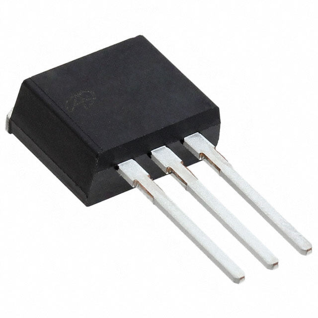
| 封装/外壳 | TO-252-3,DPak(2 引线+接片),SC-63 |
| 封装/箱体 | CPT-3 |
| 工厂包装数量 | 2500 |
| 晶体管极性 | N-Channel |
| 最大工作温度 | + 150 C |
| 最小工作温度 | - 55 C |
| 标准包装 | 1 |
| 漏源极电压(Vdss) | 60V |
| 特色产品 | http://www.digikey.com/cn/zh/ph/ROHM/MOSFET_ECOMOS.html |
| 电流-连续漏极(Id)(25°C时) | 2A (Ta) |
| 通道模式 | Enhancement |
| 配置 | Single |


- 商务部:美国ITC正式对集成电路等产品启动337调查
- 曝三星4nm工艺存在良率问题 高通将骁龙8 Gen1或转产台积电
- 太阳诱电将投资9.5亿元在常州建新厂生产MLCC 预计2023年完工
- 英特尔发布欧洲新工厂建设计划 深化IDM 2.0 战略
- 台积电先进制程称霸业界 有大客户加持明年业绩稳了
- 达到5530亿美元!SIA预计今年全球半导体销售额将创下新高
- 英特尔拟将自动驾驶子公司Mobileye上市 估值或超500亿美元
- 三星加码芯片和SET,合并消费电子和移动部门,撤换高东真等 CEO
- 三星电子宣布重大人事变动 还合并消费电子和移动部门
- 海关总署:前11个月进口集成电路产品价值2.52万亿元 增长14.8%


PDF Datasheet 数据手册内容提取
2SK2094 Transistors 4V Drive Nch MOS FET 2SK2094 (cid:122)Structure (cid:122)External dimensions (Unit : mm) Silicon N-channel MOS FET CPT3 6.5 5.1 2.3 0.5 (cid:122)Features 1.5 1) Low On-resistance. 23)) WFaidste s SwOitcAh i(nsga fsep oepeedr.a ting area). 0.9 5.5 1.59.5 4) 4V drive. 0.75 2.5 56)) PDarirvaell ecli rucsueits i sc aena sbye. simple. ((12))GDraatien 0.9(1)2.3(2) (3)0.26.53 0.8Min.01..50 (3)Source Abbreviated symbol : K2094 (cid:122)Applications Switching (cid:122)Packaging specifications (cid:122)Inner circuit Package Taping Code TL Type Basic ordering unit (pieces) 2500 2SK2094 (1) Gate (1) (2) (3) (2) Drain (3) Source (cid:122)Absolute maximum ratings (Ta=25°C) Parameter Symbol Limits Unit Drain-source voltage VDSS 60 V Gate-source voltage VGSS ±20 V Continuous ID 2 A Drain current ∗ Pulsed IDP 8 A Reverse drain Continuous IDR 2 A current Pulsed IDRP∗ 8 A Total power dissipation(Tc=25°C) PD 10 W Channel temperature Tch 150 °C Storage temperature Tstg −55 to +150 °C ∗ Pw ≤ 300µs, Duty cycle ≤ 2% Rev.A 1/4
2SK2094 Transistors (cid:122)Electrical characteristics (Ta=25°C) Parameter Symbol Min. Typ. Max. Unit Test Conditions Gate-source leakage IGSS − − ±100 nA VGS= ±20V, VDS=0V Drain-source breakdown voltage V(BR)DSS 60 − − V ID=1mA, VGS=0V Zero gate voltage drain current IDSS − − 100 µA VDS=60V, VGS=0V Gate threshold voltage VGS(th) 1.0 − 2.5 V VDS=10V, ID=1mA Sretsaitsicta dnrcaein-source on-state RDS(on) −− 00..43 00.3.55 Ω IIDD==11AA,, VVGGSS==140VV Forward transfer admittance Yfs 1.0 − − S VDS=10V, ID=1A Input capacitance Ciss − 400 − pF VDS=10V Output capacitance Coss − 150 − pF VGS=0V Reverse transfer capacitance Crss − 50 − pF f=1MHz Turn-on delay time td(on) − 10 − ns ID=1A, VDD=30V Rise time tr − 20 − ns VGS=10V Turn-off delay time td(off) − 100 − ns RL=30Ω Fall time tf − 40 − ns RG=10Ω Reverse recovery time (Body Diode) trr − 100 − ns IDR=2A, VGS=0V, di/dt=50A/µs Rev.A 2/4
2SK2094 Transistors (cid:122)Electrical characteristics curve 10 4 5 (A)AIN CURRENT : ID 000...125125 Opeirs altiiomint iend tbhiy s RarDe(Saon) DCP OW=p1e0ram1tmisosn (A)N CURRENT : ID 32 18640VVVV VGS=3VTPau=ls2e5d°C (A)N CURRENT : ID 0000.0...215215 Ta=1−27225555°°°°CCCC VPDuSl=s1e0dV DR0.05 DRAI 1 DRAI 0.02 0.02 Tc=25°C 0.01 0.01 Single pulse 0 0.005 0.10.2 0.5 1 2 5 10 20 50100 0 1 2 3 4 5 0 1 2 3 4 5 6 7 8 DRAIN-SOURCE VOLTAGE : VDS (V) DRAIN-SOURCE VOLTAGE : VDS (V) GATE-SOURCE VOLTAGE : VGS (V) Fig.1 Maximum Safe Operating Area Fig.2 Typical Output Characteristics Fig.3 Typical Transfer Characteristics (V)TE THRESHOLD VOLTAGE : VGS(th) 3214 VlDD=S1=m10AV STATIC DRAIN-SOURCE Ω ()ON-STATE RESISTANCE : RDS(on)00..000001...251251250 Ta=1−27225555°°°°CCCC VPGuSl=s1e0dV STATIC DRAIN-SOURCE Ω()ON-STATE RESISTANCE : RDS(on) 00000..001...152152250 Ta=1−27225555°°°°CCCC VPGuSl=s4eVd A G 0 0.01 0.01 −50 −25 0 25 50 75 100 125 150 0.0050.01 0.02 0.05 0.1 0.2 0.5 1 2 5 0.005 0.010.02 0.05 0.1 0.2 0.5 1 2 5 CHANNEL TEMPERATURE : Tch (°C) DRAIN CURRENT : ID (A) DRAIN CURRENT : ID (A) Fig.4 Gate Threshold Voltage Fig.5 Static Drain-Source On-State Resistance Fig.6 Static Drain-Source On-State Resistance Fig.4 vs. Channel Temperature Fig.5 vs. Drain Current ( Ι ) Fig.6 vs. Drain Current ( ΙΙ ) STATIC DRAIN-SOURCE Ω ()ON-STATE RESISTANCE : RDS(on) 000000......123456 ID=21AA TPau=ls2e5d°C STATIC DRAIN-SOURCE Ω ()ON-STATE RESISTANCE : RDS(on) 00000000........27813456 VPIDGu=Sl1=sA1e0dV (S)WARD TRANSFER ADMITTANCE : YfS 00..000001...125251250 Ta= 1−22275555°°°°CCCC VPDuSls=e1d0V 0 0 OR0.01 0 5 10 15 20 −50 −25 0 25 50 75 100 125 150 F 0.005 0.010.02 0.05 0.1 0.2 0.5 1 2 5 GATE-SOURCE VOLTAGE : VGS (V) CHANNEL TEMPERATURE : Tch (°C) DRAIN CURRENT : ID (A) Fig.7 Static Drain-Source On-State Resistance Fig.8 Static Drain-Source On-State Resistance Fig.9 Forward Transfer Admittance Fig.7 vs. Gate-Source Voltage Fig.8 vs. Channel Temperature Fig.9 vs. Drain Current Rev.A 3/4
2SK2094 Transistors (A)NT : IDR 521 Ta=12755°°CC VPGuSls=e0dV (A)NT : IDR 125 VGS= 10V 0V TPau=ls2e5d°C pF)12000000 TVPf=aGu1S=lsM=2e0H5dV°zC URRE 0.5 −2255°°CC URRE 0.5 (E : C 500 Ciss RAIN C 00..21 RAIN C 00..12 CITANC 200 Coss D D A RSE 0.05 RSE 0.05 CAP 100 VE 0.02 VE0.02 50 Crss E E R 0.01 R0.01 0.005 20 0 0.5 1 1.5 0 0.5 1 1.5 1 2 5 10 20 50 100 SOURCE-DRAIN VOLTAGE : VSD (V) SOURCE-DRAIN VOLTAGE : VSD (V) DRAIN-SOURCE VOLTAGE : VDS (V) Fig.10 Reverse Drain Current Fig.11 Reverse Drain Current Fig.12 Typical Capacitance Fig.10 vs. Source-Drain Voltage ( Ι ) Fig.11 vs. Source-Drain Voltage ( ΙΙ ) Fig.12 vs. Drain-Source Voltage 500 10 Ta=25°C VDD=30V (ns)SWITCHING TIME : t2100521000005 tdtt(froftf)d(on) PRVuGGS=ls=1e10d0ΩV NORMALIZED TRANSIENT ( t )THERMAL RESISTANCE : r 00.0.111000D00.....00=2155210.01 Tθθttchh=((cc2hh--5cc))° (=Ct6)=.2r 5(t°)C / Wθth (ch-c) Single pulse PW D=PW 02.02 0.05 0.1 0.2 0.5 1 2 5 0.00 110µ 100µ 1m 10m 100m T 1 T 10 DRAIN CURRENT : ID (A) PULSE WIDTH : PW (s) Fig.13 Switching characteristics Fig.14 Normalized Transient Thermal Resistance vs . Pulse Width (See Figure. 15 and 16 for the measurement circuit and resultant waveforms) (cid:122)Switching characteristics measurement circuit Pulse Width 90% 50% 50% VGS ID VDS VGS 10% RG D.U.T. RL VDS 10% 10% V DD 90% 90% td(on) tr td(off) tf ton toff Fig.15 Switching Time Test Circuit Fig.16 Switching Time Waveforms Rev.A 4/4
Appendix Notes No technical content pages of this document may be reproduced in any form or transmitted by any means without prior permission of ROHM CO.,LTD. The contents described herein are subject to change without notice. The specifications for the product described in this document are for reference only. Upon actual use, therefore, please request that specifications to be separately delivered. Application circuit diagrams and circuit constants contained herein are shown as examples of standard use and operation. Please pay careful attention to the peripheral conditions when designing circuits and deciding upon circuit constants in the set. Any data, including, but not limited to application circuit diagrams information, described herein are intended only as illustrations of such devices and not as the specifications for such devices. ROHM CO.,LTD. disclaims any warranty that any use of such devices shall be free from infringement of any third party's intellectual property rights or other proprietary rights, and further, assumes no liability of whatsoever nature in the event of any such infringement, or arising from or connected with or related to the use of such devices. Upon the sale of any such devices, other than for buyer's right to use such devices itself, resell or otherwise dispose of the same, no express or implied right or license to practice or commercially exploit any intellectual property rights or other proprietary rights owned or controlled by ROHM CO., LTD. is granted to any such buyer. Products listed in this document are no antiradiation design. The products listed in this document are designed to be used with ordinary electronic equipment or devices (such as audio visual equipment, office-automation equipment, communications devices, electrical appliances and electronic toys). Should you intend to use these products with equipment or devices which require an extremely high level of reliability and the malfunction of with would directly endanger human life (such as medical instruments, transportation equipment, aerospace machinery, nuclear-reactor controllers, fuel controllers and other safety devices), please be sure to consult with our sales representative in advance. About Export Control Order in Japan Products described herein are the objects of controlled goods in Annex 1 (Item 16) of Export Trade Control Order in Japan. In case of export from Japan, please confirm if it applies to "objective" criteria or an "informed" (by MITI clause) on the basis of "catch all controls for Non-Proliferation of Weapons of Mass Destruction. Appendix1-Rev1.1
Mouser Electronics Authorized Distributor Click to View Pricing, Inventory, Delivery & Lifecycle Information: R OHM Semiconductor: 2SK2094TL