ICGOO在线商城 > 分立半导体产品 > 晶体管 - 双极 (BJT) - 射频 > 2SC5087-O(TE85L,F)
.jpg)
 Datasheet下载
- 型号: 2SC5087-O(TE85L,F)
- 制造商: Toshiba America Electronic Components, Inc.
- 库位|库存: xxxx|xxxx
- 要求:
| 数量阶梯 | 香港交货 | 国内含税 |
| +xxxx | $xxxx | ¥xxxx |
查看当月历史价格
查看今年历史价格
2SC5087-O(TE85L,F)产品简介:
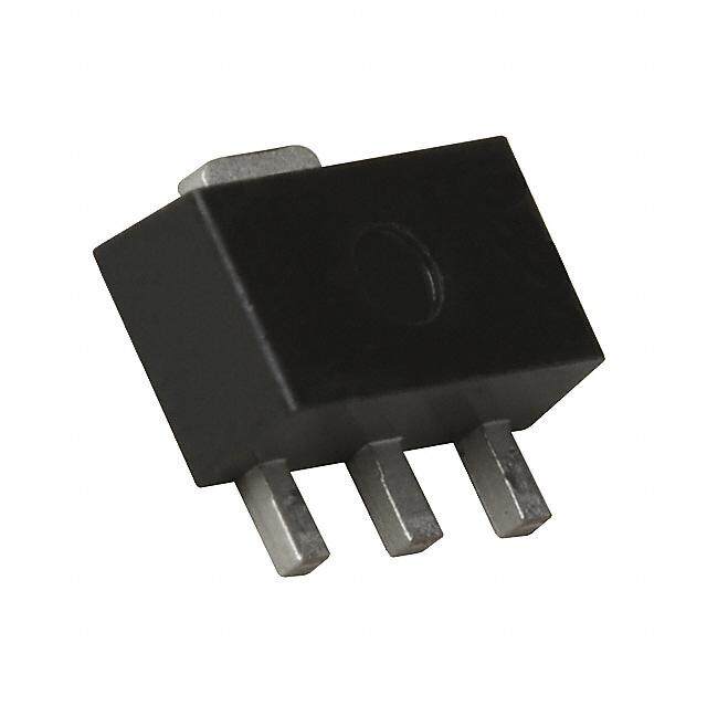
ICGOO电子元器件商城为您提供2SC5087-O(TE85L,F)由Toshiba America Electronic Components, Inc.设计生产,在icgoo商城现货销售,并且可以通过原厂、代理商等渠道进行代购。 2SC5087-O(TE85L,F)价格参考¥1.12-¥3.72。Toshiba America Electronic Components, Inc.2SC5087-O(TE85L,F)封装/规格:晶体管 - 双极 (BJT) - 射频, RF Transistor NPN 12V 80mA 7GHz 150mW 表面贴装 SMQ。您可以下载2SC5087-O(TE85L,F)参考资料、Datasheet数据手册功能说明书,资料中有2SC5087-O(TE85L,F) 详细功能的应用电路图电压和使用方法及教程。
| 参数 | 数值 |
| 产品目录 | |
| 描述 | TRANS RF NPN 12V 1MHZ SMQ射频双极晶体管 RF Device VHF/UHF 13V 150mW 13dB 7GHz |
| 产品分类 | RF 晶体管 (BJT)分离式半导体 |
| 品牌 | Toshiba Semiconductor and StorageToshiba |
| 产品手册 | http://www.toshiba.com/taec/Catalog/Product.do?productid=1922465&lineid=83&subcategoryid=1936988&familyid=900135 |
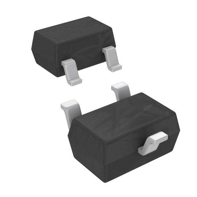
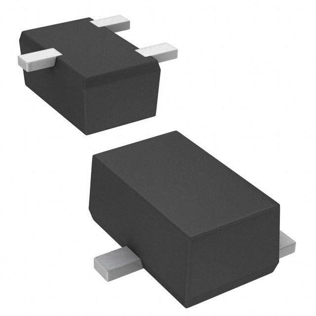
| 产品图片 |
|
| rohs | 符合RoHS无铅 / 符合限制有害物质指令(RoHS)规范要求 |
| 产品系列 | 晶体管,晶体管射频,射频双极晶体管,Toshiba 2SC5087-O(TE85L,F)- |
| 数据手册 | |
| 产品型号 | 2SC5087-O(TE85L,F)2SC5087-O(TE85L,F) |
| 不同 Ic、Vce 时的DC电流增益(hFE)(最小值) | 80 @ 20mA,10V |
| 产品种类 | 射频双极晶体管 |
| 供应商器件封装 | SMQ |
| 其它名称 | 2SC5087-O(TE85LF)CT |
| 功率-最大值 | 150mW |
| 功率耗散 | 150 mW |
| 包装 | 剪切带 (CT) |
| 发射极-基极电压VEBO | 3 V |
| 商标 | Toshiba |
| 噪声系数(dB,不同f时的典型值) | 1dB ~ 1.1dB @ 500MHz ~ 1GHz |
| 增益 | - |
| 安装类型 | 表面贴装 |
| 安装风格 | SMD/SMT |
| 封装 | Reel |
| 封装/外壳 | SC-61AA |
| 封装/箱体 | SMQ-4 |
| 工厂包装数量 | 3000 |
| 技术 | Silicon |
| 晶体管极性 | NPN |
| 晶体管类型 | NPN |
| 最大工作温度 | + 125 C |
| 最大工作频率 | 7 GHz (Typ) |
| 最小工作温度 | - 55 C |
| 标准包装 | 1 |
| 电压-集射极击穿(最大值) | 12V |
| 电流-集电极(Ic)(最大值) | 80mA |
| 直流集电极/BaseGainhfeMin | 80 |
| 类型 | VHF UHF Low Noise Low Distortion Amplifier |
| 配置 | Single |
| 集电极—发射极最大电压VCEO | 12 V |
| 集电极连续电流 | 80 mA |
| 频率 | 7 GHz (Typ) |
| 频率-跃迁 | 7GHz |


- 商务部:美国ITC正式对集成电路等产品启动337调查
- 曝三星4nm工艺存在良率问题 高通将骁龙8 Gen1或转产台积电
- 太阳诱电将投资9.5亿元在常州建新厂生产MLCC 预计2023年完工
- 英特尔发布欧洲新工厂建设计划 深化IDM 2.0 战略
- 台积电先进制程称霸业界 有大客户加持明年业绩稳了
- 达到5530亿美元!SIA预计今年全球半导体销售额将创下新高
- 英特尔拟将自动驾驶子公司Mobileye上市 估值或超500亿美元
- 三星加码芯片和SET,合并消费电子和移动部门,撤换高东真等 CEO
- 三星电子宣布重大人事变动 还合并消费电子和移动部门
- 海关总署:前11个月进口集成电路产品价值2.52万亿元 增长14.8%


PDF Datasheet 数据手册内容提取
2SC5087 TOSHIBA Transistor Silicon NPN Epitaxial Planar Type 2SC5087 VHF~UHF Band Low Noise Amplifier Applications Unit: mm • Low noise figure, high gain. • NF = 1.1dB, |S21e|2 = 13dB (f = 1 GHz) Absolute Maximum Ratings (Ta = 25°C) Characteristics Symbol Rating Unit Collector-base voltage VCBO 20 V Collector-emitter voltage VCEO 12 V Emitter-base voltage VEBO 3 V Base current IB 40 mA Collector current IC 80 mA Collector power dissipation PC 150 mW Junction temperature Tj 125 °C Storage temperature range Tstg −55 to 125 °C Note: Using continuously under heavy loads (e.g. the application of high temperature/current/voltage and the significant change in JEDEC ― temperature, etc.) may cause this product to decrease in the reliability significantly even if the operating conditions (i.e. JEITA ― operating temperature/current/voltage, etc.) are within the absolute maximum ratings. TOSHIBA 2-3J1C Please design the appropriate reliability upon reviewing the Weight: 0.012 g (typ.) Toshiba Semiconductor Reliability Handbook (“Handling Precautions”/“Derating Concept and Methods”) and individual reliability data (i.e. reliability test report and estimated failure rate, etc). Microwave Characteristics (Ta = 25°C) Characteristics Symbol Test Condition Min Typ. Max Unit Transition frequency fT VCE = 10 V, IC = 20 mA 5 7 ⎯ GHz 2 ⎪S21e⎪ (1) VCE = 10 V, IC = 20 mA, f = 500 MHz ⎯ 18 ⎯ Insertion gain dB 2 ⎪S21e⎪ (2) VCE = 10 V, IC = 20 mA, f = 1 GHz 9.5 13 ⎯ NF (1) VCE = 10 V, IC = 5 mA, f = 500 MHz ⎯ 1 ⎯ Noise figure dB NF (2) VCE = 10 V, IC = 5 mA, f = 1 GHz ⎯ 1.1 2 Electrical Characteristics (Ta = 25°C) Characteristics Symbol Test Condition Min Typ. Max Unit Collector cut-off current ICBO VCB = 10 V, IE = 0 ⎯ ⎯ 1 μA Emitter cut-off current IEBO VEB = 1 V, IC = 0 ⎯ ⎯ 1 μA hFE DC current gain VCE = 10 V, IC = 20 mA 80 ⎯ 240 (Note 1) Output capacitance Cob ⎯ 1.1 1.6 pF VCB = 10 V, IE = 0, f = 1 MHz (Note 2) Reverse transfer capacitance Cre ⎯ 0.65 1.05 pF Note 1: hFE classification O: 80 to 160, Y: 120 to 240 Note 2: Cre is measured by 3 terminal method with capacitance bridge. Start of commercial production 1993-10 1 2014-03-01
2SC5087 Marking 2 1 Type Name hFE Rank C O 3 4 2 2014-03-01
2SC5087 hFE – IC F) Cob, Cre – VCB 1000 (p 10 N hFE 530000 VTaC =E 2=5 1°C0 V (pF)ob C CEre 53 fT a= =1 2M5H°Cz NT GAI 200 CNSEPACITAN 2 Cob URRE 100 PACITAER CA 1 Cre DC C 5700 UT CARANSF 00..57 PT 301 2 3 5 7 10 20 30 50 70 100 OUTRSE 0.30.1 0.2 0.3 0.5 0.7 1 2 3 5 7 10 E COLLECTOR CURRENT IC (mA) EV COLLECTOR-BASE VOLTAGE VCB (V) R 2 fT – IC ⎪S21e⎪ – IC 10 16 GHz) VTaC =E 2=5 1°C0 V dB) Vf =C E1 G= H10z V (fT 8 2 (⎪e 12 Ta = 25°C 1 CY 6 S⎪2 N UE N 8 Q AI E 4 G R N TION F 2 ERTIO 4 SI S N N A I R 0 0 T 1 3 5 7 10 30 50 70 100 1 3 5 7 10 30 50 70 100 COLLECTOR CURRENT IC (mA) COLLECTOR CURRENT IC (mA) 2 ⎪S21e⎪ – f NF – IC 35 5 B) VCE = 10 V VCE = 10 V 2 (d⎪e 30 ITCa == 2205 °mCA (dB) 4 fT a= =1 2G5H°Cz S⎪21 20 NF 3 N RE AI U G G 2 N FI RTIO 10 OISE 1 E N S N I 0 0 0.1 0.3 0.5 0.7 0 3 5 7 10 1 3 5 7 10 30 50 70 100 FREQUENCY f (GHz) COLLECTOR CURRENT IC (mA) 3 2014-03-01
2SC5087 2 ⎪S21e⎪ – VCE PC – Ta B) 16 mW) 200 (d 14 (C 160 2 12 P ⎪1e N S⎪2 10 TIO 120 N 8 SIPA GAI DIS 80 N 6 R O WE TI 4 O R P 40 SE 2 IC = 20 mA OR N f = 1 GHz T I C Ta = 25°C E 0 L 0 0 2 4 6 8 10 12 L 0 25 50 75 100 125 150 O C COLLECTOR-EMITTER VOLTAGE VCE (V) AMBIENT TEMPERATURE Ta (°C) S-Parameter Z = 50 Ω, Ta = 25°C O V = 10 V, I = 5 mA CE C Frequency S11 S21 S12 S22 MHz Mag. Ang. Mag. Ang. Mag. Ang. Mag. Ang. 200 0.793 −82.4 11.923 133.4 0.050 52.7 0.788 −36.4 400 0.736 −128.0 7.835 108.5 0.066 38.0 0.584 −53.4 600 0.719 −152.1 5.578 94.5 0.071 34.1 0.490 −63.5 800 0.701 −168.6 4.279 84.4 0.073 33.9 0.445 −72.2 1000 0.698 178.9 3.451 76.6 0.074 36.7 0.424 −80.5 1200 0.697 168.3 2.855 69.9 0.076 40.8 0.413 −88.9 1400 0.699 159.4 2.440 64.0 0.078 46.6 0.404 −97.3 1600 0.703 150.8 2.121 59.3 0.084 52.5 0.401 −105.4 1800 0.713 142.9 1.876 54.5 0.091 58.3 0.398 −112.6 2000 0.722 134.7 1.681 50.3 0.100 63.5 0.398 −119.6 V = 10 V, I = 20 mA CE C Frequency S11 S21 S12 S22 MHz Mag. Ang. Mag. Ang. Mag. Ang. Mag. Ang. 200 0.655 −129.4 20.724 113.2 0.031 48.0 0.496 −59.6 400 0.650 −161.5 11.288 95.5 0.040 50.4 0.319 −74.1 600 0.660 −176.3 7.643 86.4 0.049 56.4 0.263 −83.5 800 0.666 172.8 5.758 79.6 0.059 60.0 0.242 −92.9 1000 0.667 164.0 4.605 74.2 0.070 63.6 0.233 −102.0 1200 0.668 156.8 3.809 69.3 0.080 65.9 0.229 −111.0 1400 0.677 148.4 3.277 65.1 0.091 68.2 0.226 −119.1 1600 0.676 141.1 2.862 61.2 0.104 70.0 0.223 −126.5 1800 0.688 133.9 2.559 57.5 0.117 71.2 0.220 −132.4 2000 0.690 126.7 2.303 54.1 0.131 72.4 0.217 −137.8 4 2014-03-01
2SC5087 S11e S21e VCE = 10 V VCE = 10 V IC = 5 mA IC = 5 mA Ta = 25°C Ta = 25°C (Unit: Ω) j50 90° 120° 60° j25 j100 16 2.0 j150 12 150° j10 f = 0.2 GHz 0.4 30° 1.6 j250 8 0.8 2 1.2 1.2 1.6 0 10 25 50 100 250 ±180° 16 12 8 4 2.00 0° 0.8 −j10 −j250 −150° −30° 0.4 −j150 f = 0.2 GHz −j25 −j100 −120° −60° −j50 −90° S12e S22e VCE = 10 V VCE = 10 V IC = 5 mA IC = 5 mA Ta = 25°C Ta = 25°C 90° (Unit: Ω) j50 0.20 120° 60° 0.16 j25 j100 0.12 j150 150° 30° 2.0 j10 0.08 1.6 j250 f = 0.2 GHz 1.2 0.04 0.8 0.4 ±180°0 .20 0.16 0.12 0.08 0.04 0 0° 0 10 25 50 100 250 2.0 1.2 −150° −30° −j10 1.6 0.8 0.4 f = 0.2 GHz −j250 −j150 −j25 −j100 −120° −60° −90° −j50 5 2014-03-01
2SC5087 S11e S21e VCE = 10 V VCE = 10 V IC = 20 mA IC = 20 mA Ta = 25°C Ta = 25°C (Unit: Ω) j50 90° 120° 60° j25 j100 20 2.0 j150 150° f = 0.2 GHz 15 j10 1.6 0.4 30° j250 10 1.2 0.8 5 1.2 0 0.8 10 25 50 100 250 ±180° 20 15 10 5 0 21.0.6 0° 0.4 −j10 −j250 f = 0.2 GHz −150° −30° −j150 −j25 −j100 −120° −60° −j50 −90° S12e S22e VCE = 10 V VCE = 10 V IC = 20 mA IC = 20 mA Ta = 25°C Ta = 25°C 90° (Unit: Ω) j50 0.20 120° 60° 0.16 j25 j100 2.0 0.12 j150 150° 1.6 30° 0.08 1.2 j10 j250 0.04 0.4 0.8 ±180°0 .20 0.16 0.12 0.08 0.04 0f = 0.2 GHz 0° 0 10 252.0 50 100 250 1.6 0.8 1.2 0.4 −j10 −j250 −150° −30° f = 0.2 GHz −j150 −j25 −j100 −120° −60° −90° −j50 6 2014-03-01
2SC5087 RESTRICTIONS ON PRODUCT USE • Toshiba Corporation, and its subsidiaries and affiliates (collectively "TOSHIBA"), reserve the right to make changes to the information in this document, and related hardware, software and systems (collectively "Product") without notice. • This document and any information herein may not be reproduced without prior written permission from TOSHIBA. Even with TOSHIBA's written permission, reproduction is permissible only if reproduction is without alteration/omission. • Though TOSHIBA works continually to improve Product's quality and reliability, Product can malfunction or fail. Customers are responsible for complying with safety standards and for providing adequate designs and safeguards for their hardware, software and systems which minimize risk and avoid situations in which a malfunction or failure of Product could cause loss of human life, bodily injury or damage to property, including data loss or corruption. Before customers use the Product, create designs including the Product, or incorporate the Product into their own applications, customers must also refer to and comply with (a) the latest versions of all relevant TOSHIBA information, including without limitation, this document, the specifications, the data sheets and application notes for Product and the precautions and conditions set forth in the "TOSHIBA Semiconductor Reliability Handbook" and (b) the instructions for the application with which the Product will be used with or for. Customers are solely responsible for all aspects of their own product design or applications, including but not limited to (a) determining the appropriateness of the use of this Product in such design or applications; (b) evaluating and determining the applicability of any information contained in this document, or in charts, diagrams, programs, algorithms, sample application circuits, or any other referenced documents; and (c) validating all operating parameters for such designs and applications. TOSHIBA ASSUMES NO LIABILITY FOR CUSTOMERS' PRODUCT DESIGN OR APPLICATIONS. • PRODUCT IS NEITHER INTENDED NOR WARRANTED FOR USE IN EQUIPMENTS OR SYSTEMS THAT REQUIRE EXTRAORDINARILY HIGH LEVELS OF QUALITY AND/OR RELIABILITY, AND/OR A MALFUNCTION OR FAILURE OF WHICH MAY CAUSE LOSS OF HUMAN LIFE, BODILY INJURY, SERIOUS PROPERTY DAMAGE AND/OR SERIOUS PUBLIC IMPACT ("UNINTENDED USE"). Except for specific applications as expressly stated in this document, Unintended Use includes, without limitation, equipment used in nuclear facilities, equipment used in the aerospace industry, medical equipment, equipment used for automobiles, trains, ships and other transportation, traffic signaling equipment, equipment used to control combustions or explosions, safety devices, elevators and escalators, devices related to electric power, and equipment used in finance-related fields. IF YOU USE PRODUCT FOR UNINTENDED USE, TOSHIBA ASSUMES NO LIABILITY FOR PRODUCT. For details, please contact your TOSHIBA sales representative. • Do not disassemble, analyze, reverse-engineer, alter, modify, translate or copy Product, whether in whole or in part. • Product shall not be used for or incorporated into any products or systems whose manufacture, use, or sale is prohibited under any applicable laws or regulations. • The information contained herein is presented only as guidance for Product use. No responsibility is assumed by TOSHIBA for any infringement of patents or any other intellectual property rights of third parties that may result from the use of Product. No license to any intellectual property right is granted by this document, whether express or implied, by estoppel or otherwise. • ABSENT A WRITTEN SIGNED AGREEMENT, EXCEPT AS PROVIDED IN THE RELEVANT TERMS AND CONDITIONS OF SALE FOR PRODUCT, AND TO THE MAXIMUM EXTENT ALLOWABLE BY LAW, TOSHIBA (1) ASSUMES NO LIABILITY WHATSOEVER, INCLUDING WITHOUT LIMITATION, INDIRECT, CONSEQUENTIAL, SPECIAL, OR INCIDENTAL DAMAGES OR LOSS, INCLUDING WITHOUT LIMITATION, LOSS OF PROFITS, LOSS OF OPPORTUNITIES, BUSINESS INTERRUPTION AND LOSS OF DATA, AND (2) DISCLAIMS ANY AND ALL EXPRESS OR IMPLIED WARRANTIES AND CONDITIONS RELATED TO SALE, USE OF PRODUCT, OR INFORMATION, INCLUDING WARRANTIES OR CONDITIONS OF MERCHANTABILITY, FITNESS FOR A PARTICULAR PURPOSE, ACCURACY OF INFORMATION, OR NONINFRINGEMENT. • Do not use or otherwise make available Product or related software or technology for any military purposes, including without limitation, for the design, development, use, stockpiling or manufacturing of nuclear, chemical, or biological weapons or missile technology products (mass destruction weapons). Product and related software and technology may be controlled under the applicable export laws and regulations including, without limitation, the Japanese Foreign Exchange and Foreign Trade Law and the U.S. Export Administration Regulations. Export and re-export of Product or related software or technology are strictly prohibited except in compliance with all applicable export laws and regulations. • Please contact your TOSHIBA sales representative for details as to environmental matters such as the RoHS compatibility of Product. Please use Product in compliance with all applicable laws and regulations that regulate the inclusion or use of controlled substances, including without limitation, the EU RoHS Directive. TOSHIBA ASSUMES NO LIABILITY FOR DAMAGES OR LOSSES OCCURRING AS A RESULT OF NONCOMPLIANCE WITH APPLICABLE LAWS AND REGULATIONS. 7 2014-03-01