ICGOO在线商城 > 分立半导体产品 > 晶体管 - 双极 (BJT) - 单 > 2N6045
 Datasheet下载
- 型号: 2N6045
- 制造商: Central Semiconductor
- 库位|库存: xxxx|xxxx
- 要求:
| 数量阶梯 | 香港交货 | 国内含税 |
| +xxxx | $xxxx | ¥xxxx |
查看当月历史价格
查看今年历史价格
2N6045产品简介:
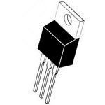
ICGOO电子元器件商城为您提供2N6045由Central Semiconductor设计生产,在icgoo商城现货销售,并且可以通过原厂、代理商等渠道进行代购。 2N6045价格参考¥6.12-¥10.25。Central Semiconductor2N6045封装/规格:晶体管 - 双极 (BJT) - 单, 双极 (BJT) 晶体管 NPN - 达林顿 100V 8A 75W 通孔 TO-220AB。您可以下载2N6045参考资料、Datasheet数据手册功能说明书,资料中有2N6045 详细功能的应用电路图电压和使用方法及教程。
| 参数 | 数值 |
| 品牌 | Central Semiconductor |
| 产品目录 | 半导体 |
| 描述 | 达林顿晶体管 NPN Darl SW |
| 产品分类 | 分离式半导体 |
| 产品手册 | |
| 产品图片 |
|
| rohs | 符合RoHS |
| 产品系列 | 晶体管,达林顿晶体管,Central Semiconductor 2N6045 |
| 产品型号 | 2N6045 |
| 产品种类 | |
| 功率耗散 | 75 W |
| 发射极-基极电压VEBO | 5 V |
| 商标 | Central Semiconductor |
| 安装风格 | Through Hole |
| 封装 | Bulk |
| 封装/箱体 | TO-220 |
| 工厂包装数量 | 400 |
| 晶体管极性 | NPN |
| 最大工作温度 | + 150 C |
| 最大直流电集电极电流 | 10 A |
| 最大集电极截止电流 | 20 uA |
| 最小工作温度 | - 65 C |
| 直流集电极/BaseGainhfeMin | 1000 |
| 系列 | 2N6045 |
| 配置 | Single |
| 集电极—发射极最大电压VCEO | 100 V |
| 集电极—基极电压VCBO | 100 V |
| 集电极连续电流 | 8 A |


- 商务部:美国ITC正式对集成电路等产品启动337调查
- 曝三星4nm工艺存在良率问题 高通将骁龙8 Gen1或转产台积电
- 太阳诱电将投资9.5亿元在常州建新厂生产MLCC 预计2023年完工
- 英特尔发布欧洲新工厂建设计划 深化IDM 2.0 战略
- 台积电先进制程称霸业界 有大客户加持明年业绩稳了
- 达到5530亿美元!SIA预计今年全球半导体销售额将创下新高
- 英特尔拟将自动驾驶子公司Mobileye上市 估值或超500亿美元
- 三星加码芯片和SET,合并消费电子和移动部门,撤换高东真等 CEO
- 三星电子宣布重大人事变动 还合并消费电子和移动部门
- 海关总署:前11个月进口集成电路产品价值2.52万亿元 增长14.8%


PDF Datasheet 数据手册内容提取
PNP - 2N6040, 2N6042, NPN - 2N6043, 2N6045 Plastic Medium-Power Complementary Silicon Transistors www.onsemi.com Plastic medium−power complementary silicon transistors are designed for general−purpose amplifier and low−speed switching DARLINGTON, 8 AMPERES applications. COMPLEMENTARY SILICON Features • POWER TRANSISTORS High DC Current Gain − h = 2500 (Typ) @ I = 4.0 Adc FE C • 60 − 100 VOLTS, 75 WATTS Collector−Emitter Sustaining Voltage − @ 100 mAdc − V = 60 Vdc (Min) − 2N6040, 2N6043 CEO(sus) = 100 Vdc (Min) − 2N6042, 2N6045 • Low Collector−Emitter Saturation Voltage − V = 2.0 Vdc (Max) @ I = 4.0 Adc − 2N6043,44 CE(sat) C = 2.0 Vdc (Max) @ I = 3.0 Adc − 2N6042, 2N6045 C • Monolithic Construction with Built−In Base−Emitter Shunt Resistors • Epoxy Meets UL 94 V−0 @ 0.125 in • ESD Ratings: Human Body Model, 3B > 8000 V Machine Model, C > 400 V • These Devices are Pb−Free and are RoHS Compliant* TO−220 CASE 221A STYLE 1 MAXIMUM RATINGS (Note 1) Rating Symbol Value Unit MARKING DIAGRAM Collector−Emitter Voltage 2N6040 VCEO 60 Vdc 2N6043 2N6042 100 2N6045 Collector−Base Voltage 2N6040 VCB 60 Vdc 2N6043 2N6042 100 2N604xG 2N6045 AYWW Emitter−Base Voltage VEB 5.0 Vdc Collector Current Continuous IC 8.0 Adc Peak 16 Base Current IB 120 mAdc Total Power Dissipation @ TC = 25°C PD 75 W 2N604x =Device Code Derate above 25°C 0.60 W/°C x = 0, 2, 3, or 5 A = Assembly Location Operating and Storage Junction TJ, Tstg –65 to +150 °C Y = Year Temperature Range WW = Work Week Stresses exceeding those listed in the Maximum Ratings table may damage the G = Pb−Free Package device. If any of these limits are exceeded, device functionality should not be assumed, damage may occur and reliability may be affected. 1. Indicates JEDEC Registered Data. ORDERING INFORMATION See detailed ordering and shipping information in the package dimensions section on page 5 of this data sheet. *For additional information on our Pb−Free strategy and soldering details, please download the ON Semiconductor Soldering and Mounting Techniques Reference Manual, SOLDERRM/D. © Semiconductor Components Industries, LLC, 2014 1 Publication Order Number: November, 2014 − Rev. 10 2N6040/D
PNP − 2N6040, 2N6042, NPN − 2N6043, 2N6045 ÎÎÎÎÎÎÎÎÎÎÎÎÎÎÎÎÎÎÎÎÎÎÎÎÎÎÎÎÎÎÎÎÎ THERMAL CHARACTERISTICS ÎÎÎÎÎÎÎÎÎÎÎÎÎÎÎÎÎÎÎÎÎÎÎÎÎÎÎÎÎÎÎÎÎÎÎÎÎÎÎÎÎÎÎÎÎÎÎÎÎÎÎÎÎÎÎÎÎÎÎÎÎÎÎÎÎÎÎÎÎ ÎÎÎÎÎÎÎÎÎÎÎÎÎÎÎÎÎÎÎÎCÎÎharaÎÎcterÎÎisticÎÎÎÎÎÎÎÎÎÎÎÎÎÎÎÎÎÎÎÎÎÎÎÎSymÎÎbolÎÎÎÎÎÎÎÎMÎÎax ÎÎÎÎÎÎÎÎUniÎÎt Thermal Resistance, Junction−to−Case (cid:2) 1.67 °C/W ÎÎÎÎÎÎÎÎÎÎÎÎÎÎÎÎÎÎÎÎÎÎÎÎÎÎÎÎÎÎÎÎÎÎÎÎÎÎÎÎÎÎÎÎÎÎÎÎÎÎJÎÎC ÎÎÎÎÎÎÎÎÎÎÎÎÎÎÎÎÎÎÎÎ Thermal Resistance, Junction−to−Ambient (cid:2) 57 °C/W ÎÎÎÎÎÎÎÎÎÎÎÎÎÎÎÎÎÎÎÎÎÎÎÎÎJÎA ÎÎÎÎÎÎÎÎÎÎ *ELECTRICAL CHARACTERISTICS (TC = 25°C unless otherwise noted) Characteristic Symbol Min Max Unit OFF CHARACTERISTICS Collector−Emitter Sustaining Voltage VCEO(sus) Vdc (IC = 100 mAdc, IB = 0) 2N6040, 2N6043 60 − 2N6042, 2N6045 100 − Collector Cutoff Current ICEO (cid:3)A (VCE = 60 Vdc, IB = 0) 2N6040, 2N6043 − 20 (VCE = 100 Vdc, IB = 0) 2N6042, 2N6045 − 20 Collector Cutoff Current ICEX (cid:3)A (VCE = 60 Vdc, VBE(off) = 1.5 Vdc) 2N6040, 2N6043 − 20 (VCE = 100 Vdc, VBE(off) = 1.5 Vdc) 2N6042, 2N6045 − 20 (VCE = 60 Vdc, VBE(off) = 1.5 Vdc, TC = 150°C) 2N6040, 2N6043 − 200 (VCE = 80 Vdc, VBE(off) = 1.5 Vdc, TC = 150°C) 2N6041, 2N6044 − 200 (VCE = 100 Vdc, VBE(off) = 1.5 Vdc, TC = 150°C) 2N6042, 2N6045 − 200 Collector Cutoff Current ICBO (cid:3)A (VCB = 60 Vdc, IE = 0) 2N6040, 2N6043 − 20 (VCB = 100 Vdc, IE = 0) 2N6042, 2N6045 − 20 Emitter Cutoff Current (VBE = 5.0 Vdc, IC = 0) IEBO − 2.0 mAdc ON CHARACTERISTICS DC Current Gain hFE − (IC = 4.0 Adc, VCE = 4.0 Vdc) 2N6040, 2N6043, 1000 20.000 (IC = 3.0 Adc, VCE = 4.0 Vdc) 2N6042, 2N6045 1000 20,000 (IC = 8.0 Adc, VCE = 4.0 Vdc) All Types 100 − Collector−Emitter Saturation Voltage VCE(sat) Vdc (IC = 4.0 Adc, IB = 16 mAdc) 2N6040, 2N6043, − 2.0 (IC = 3.0 Adc, IB = 12 mAdc) 2N6042, 2N6045 − 2.0 (IC = 8.0 Adc, IB = 80 Adc) All Types − 4.0 Base−Emitter Saturation Voltage (IC = 8.0 Adc, IB = 80 mAdc) VBE(sat) − 4.5 Vdc Base−Emitter On Voltage (IC = 4.0 Adc, VCE = 4.0 Vdc) VBE(on) − 2.8 Vdc DYNAMIC CHARACTERISTICS Small Signal Current Gain (IC = 3.0 Adc, VCE = 4.0 Vdc, f = 1.0 MHz) |hfe| 4.0 − Output Capacitance 2N6040/2N6042 Cob − 300 pF (VCB = 10 Vdc, IE = 0, f = 0.1 MHz) 2N6043/2N6045 − 200 Small−Signal Current Gain (IC = 3.0 Adc, VCE = 4.0 Vdc, f = 1.0 kHz) hfe 300 − − Product parametric performance is indicated in the Electrical Characteristics for the listed test conditions, unless otherwise noted. Product performance may not be indicated by the Electrical Characteristics if operated under different conditions. *Indicates JEDEC Registered Data. http://onsemi.com 2
PNP − 2N6040, 2N6042, NPN − 2N6043, 2N6045 TA TC 4.0 80 S) T T A 3.0 60 W N ( O SIPATI 2.0 40 TC S DI R WE TA O 1.0 20 P , D P 0 0 0 20 40 60 80 100 120 140 160 T, TEMPERATURE (°C) Figure 1. Power Derating 5.0 3.0 ts RB & RC VARIED TO OBTAIN DESIRED CURRENT LEVELS -V(cid:4)3C0C V 2.0 D1 MUST BE FAST RECOVERY TYPE, eg: (cid:2)(cid:2)1MNS5D862150 U0 SUESDE DA BBOEVLEO WIB ≈IB 1≈0 100 m0A mA TUTRC SCOPE μ(cid:2)(cid:3)s) 10..07 tf V2 RB ME ( 0.5 approx TI +(cid:4)8.0 V 51 D1 ≈ 8.0 k ≈(cid:3)120 t, 00..32 VCC = 30 V tr 0 IC/IB = 250 apVp1rox +(cid:4)4.0 V 0.1 ITBJ1 == 2IB52°C -12 V 25 (cid:3)s for td and tr, D1 is disconnected 0.07 PNNPPN td @ VBE(off) = 0 V tr, tf ≤ 10 ns aFnodr NVP2 N= t0est circuit reverse all polarities and D1. 0.050.1 0.2 0.3 0.5 0.7 1.0 2.0 3.0 5.0 7.0 10 DUTY CYCLE = 1.0% IC, COLLECTOR CURRENT (AMP) Figure 2. Switching Times Equivalent Circuit Figure 3. Switching Times 1.0 D) 0.7 D = 0.5 E Z 0.5 r(t), EFFECTIVE TRANSIENTRMAL RESISTANCE (NORMALI000000...000...213573 S00IN..00G52L00E..21 PULSE 0.01 (cid:2)(cid:2)DPRTJJJU EC(CCpLA( Uk=StD)) R E- 1=TV . TT6IrEM(CR7tS) °EA = C(cid:2)A I ANPJ/PWTC( PpS tkL1H)Y (cid:2)O FJWCO(NtR) POWER P(pk)DUTtY1 CtY2CLE, D = t1/t2 E0.02 H T 0.01 0.01 0.020.03 0.05 0.1 0.2 0.3 0.5 1.0 2.0 3.0 5.0 10 20 30 50 100 200 300 500 1000 t, TIME OR PULSE WIDTH (ms) Figure 4. Thermal Response http://onsemi.com 3
PNP − 2N6040, 2N6042, NPN − 2N6043, 2N6045 20 There are two limitations on the power handling ability of 100 (cid:3)s 10 a transistor: average junction temperature and second P) breakdown. Safe operating area curves indicate I − V M5.0 C CE T (A 5001 .(cid:3)0(cid:3)sms limits of the transistor that must be observed for reliable URREN21..00 BTOJ N= D1I5N0G°C WIRE LIM5.I0T(cid:3)EmDs dc odipsesriaptaitoino;n i .teh.a, nth teh etr acnusrivsetosr i nmduiscta nteo.t be subjected to greater OR C0.5 THERMALLY LIMITED @ TC = 25°C The data of Figure 5 is based on TJ(pk) = 150°C; TC is T (SINGLE PULSE) variable depending on conditions. Second breakdown pulse C LE0.2 SECOND BREAKDOWN LIMITED limits are valid for duty cycles to 10% provided TJ(pk) COL0.1 CURVES APPLY BELOW RATED VCEO < 150°C. TJ(pk) may be calculated from the data in Figure 4. , C 2N6040, 2N6043 At high case temperatures, thermal limitations will reduce I0.05 2N6045 the power that can be handled to values less than the 0.02 limitations imposed by second breakdown. 1.0 2.0 3.0 5.0 7.0 10 20 30 50 70 100 VCE, COLLECTOR-EMITTER VOLTAGE (VOLTS) Figure 5. Active−Region Safe Operating Area 10,000 300 N 5000 TJ = 25°C GAI 3000 200 T 2000 N E F) R 1000 p MALL-SIGNAL CUR 532100000000 TVICCC = E= 3 =2. 054 °.A0C dVcdc C, CAPACITANCE (17000 Cib Cob h, Sfe 532000 PNNPPN 50 PNP NPN 100 10 30 1.0 2.0 5.0 10 20 50 100 200 500 1000 0.1 0.2 0.5 1.0 2.0 5.0 10 20 50 f, FREQUENCY (kHz) VR, REVERSE VOLTAGE (VOLTS) Figure 6. Small−Signal Current Gain Figure 7. Capacitance PNP NPN 2N6040, 2N6042 2N6043, 2N6045 20,000 20,000 VCE = 4.0 V VCE = 4.0 V 10,000 10,000 N 7000 N 7000 T GAI 5000 TJ = 150°C T GAI 5000 TJ = 150°C EN 3000 EN 3000 R R UR 2000 25°C UR 2000 C C C C 25°C , DE1000 , DE1000 F 700 F 700 h 500 -(cid:4)55°C h 500 -(cid:4)55°C 300 300 200 200 0.1 0.2 0.3 0.5 0.7 1.0 2.0 3.0 5.0 7.0 10 0.1 0.2 0.3 0.5 0.7 1.0 2.0 3.0 5.0 7.0 10 IC, COLLECTOR CURRENT (AMP) IC, COLLECTOR CURRENT (AMP) Figure 8. DC Current Gain http://onsemi.com 4
PNP − 2N6040, 2N6042, NPN − 2N6043, 2N6045 S) 3.0 S) 3.0 T T VOL TJ = 25°C VOL TJ = 25°C E ( 2.6 E ( 2.6 G G A A OLT IC = 2.0 A 4.0 A 6.0 A OLT IC = 2.0 A 4.0 A 6.0 A V V R 2.2 R 2.2 E E T T T T MI MI -E 1.8 -E 1.8 R R O O T T C C E E L 1.4 L 1.4 L L O O C C , E , E C C V 1.0 V 1.0 0.3 0.5 0.7 1.0 2.0 3.0 5.0 7.0 10 20 30 0.3 0.5 0.7 1.0 2.0 3.0 5.0 7.0 10 20 30 IB, BASE CURRENT (mA) IB, BASE CURRENT (mA) Figure 9. Collector Saturation Region 3.0 3.0 TJ = 25°C TJ = 25°C 2.5 2.5 S) S) T T L L O 2.0 O 2.0 V V E ( E ( G G A A OLT 1.5 VBE @ VCE = 4.0 V OLT 1.5 VBE(sat) @ IC/IB = 250 V V V, V, VBE(sat) @ IC/IB = 250 VBE @ VCE = 4.0 V 1.0 1.0 VCE(sat) @ IC/IB = 250 VCE(sat) @ IC/IB = 250 0.5 0.5 0.1 0.2 0.3 0.5 0.7 1.0 2.0 3.0 5.0 7.010 0.1 0.2 0.3 0.5 0.7 1.0 2.0 3.0 5.0 7.0 10 IC, COLLECTOR CURRENT (AMP) IC, COLLECTOR CURRENT (AMP) Figure 10. “On” Voltages ORDERING INFORMATION Device Package Shipping 2N6040G TO−220 50 Units / Rail (Pb−Free) 2N6042G TO−220 50 Units / Rail (Pb−Free) 2N6043G TO−220 50 Units / Rail (Pb−Free) 2N6045G TO−220 50 Units / Rail (Pb−Free) http://onsemi.com 5
PNP − 2N6040, 2N6042, NPN − 2N6043, 2N6045 PACKAGE DIMENSIONS TO−220 CASE 221A−09 ISSUE AH NOTES: 1. DIMENSIONING AND TOLERANCING PER ANSI Y14.5M, 1982. −T− SPELAATNIENG 2. CONTROLLING DIMENSION: INCH. 3. DIMENSION Z DEFINES A ZONE WHERE ALL B F C BODY AND LEAD IRREGULARITIES ARE T S ALLOWED. INCHES MILLIMETERS 4 DIM MIN MAX MIN MAX A 0.570 0.620 14.48 15.75 Q A B 0.380 0.415 9.66 10.53 C 0.160 0.190 4.07 4.83 1 2 3 U D 0.025 0.038 0.64 0.96 F 0.142 0.161 3.61 4.09 H G 0.095 0.105 2.42 2.66 H 0.110 0.161 2.80 4.10 K J 0.014 0.024 0.36 0.61 Z K 0.500 0.562 12.70 14.27 L 0.045 0.060 1.15 1.52 N 0.190 0.210 4.83 5.33 L R Q 0.100 0.120 2.54 3.04 R 0.080 0.110 2.04 2.79 V J S 0.045 0.055 1.15 1.39 T 0.235 0.255 5.97 6.47 G U 0.000 0.050 0.00 1.27 D V 0.045 --- 1.15 --- Z --- 0.080 --- 2.04 N STYLE 1: PIN 1. BASE 2. COLLECTOR 3. EMITTER 4. COLLECTOR ON Semiconductor and the are registered trademarks of Semiconductor Components Industries, LLC (SCILLC) or its subsidiaries in the United States and/or other countries. SCILLC owns the rights to a number of patents, trademarks, copyrights, trade secrets, and other intellectual property. A listing of SCILLC’s product/patent coverage may be accessed at www.onsemi.com/site/pdf/Patent−Marking.pdf. SCILLC reserves the right to make changes without further notice to any products herein. SCILLC makes no warranty, representation or guarantee regarding the suitability of its products for any particular purpose, nor does SCILLC assume any liability arising out of the application or use of any product or circuit, and specifically disclaims any and all liability, including without limitation special, consequential or incidental damages. “Typical” parameters which may be provided in SCILLC data sheets and/or specifications can and do vary in different applications and actual performance may vary over time. All operating parameters, including “Typicals” must be validated for each customer application by customer’s technical experts. SCILLC does not convey any license under its patent rights nor the rights of others. SCILLC products are not designed, intended, or authorized for use as components in systems intended for surgical implant into the body, or other applications intended to support or sustain life, or for any other application in which the failure of the SCILLC product could create a situation where personal injury or death may occur. Should Buyer purchase or use SCILLC products for any such unintended or unauthorized application, Buyer shall indemnify and hold SCILLC and its officers, employees, subsidiaries, affiliates, and distributors harmless against all claims, costs, damages, and expenses, and reasonable attorney fees arising out of, directly or indirectly, any claim of personal injury or death associated with such unintended or unauthorized use, even if such claim alleges that SCILLC was negligent regarding the design or manufacture of the part. SCILLC is an Equal Opportunity/Affirmative Action Employer. This literature is subject to all applicable copyright laws and is not for resale in any manner. PUBLICATION ORDERING INFORMATION LITERATURE FULFILLMENT: N. American Technical Support: 800−282−9855 Toll Free ON Semiconductor Website: www.onsemi.com Literature Distribution Center for ON Semiconductor USA/Canada P.O. Box 5163, Denver, Colorado 80217 USA Europe, Middle East and Africa Technical Support: Order Literature: http://www.onsemi.com/orderlit Phone: 303−675−2175 or 800−344−3860 Toll Free USA/Canada Phone: 421 33 790 2910 Fax: 303−675−2176 or 800−344−3867 Toll Free USA/Canada Japan Customer Focus Center For additional information, please contact your local Email: orderlit@onsemi.com Phone: 81−3−5817−1050 Sales Representative http://onsemi.com 2N6040/D 6