ICGOO在线商城 > 分立半导体产品 > 晶体管 - 双极 (BJT) - 单 > 2N5320
 Datasheet下载
- 型号: 2N5320
- 制造商: Central Semiconductor
- 库位|库存: xxxx|xxxx
- 要求:
| 数量阶梯 | 香港交货 | 国内含税 |
| +xxxx | $xxxx | ¥xxxx |
查看当月历史价格
查看今年历史价格
2N5320产品简介:
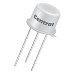
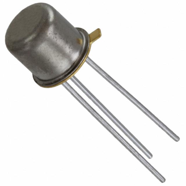
ICGOO电子元器件商城为您提供2N5320由Central Semiconductor设计生产,在icgoo商城现货销售,并且可以通过原厂、代理商等渠道进行代购。 2N5320价格参考。Central Semiconductor2N5320封装/规格:晶体管 - 双极 (BJT) - 单, 双极 (BJT) 晶体管 NPN 75V 2A 10W 通孔 TO-39。您可以下载2N5320参考资料、Datasheet数据手册功能说明书,资料中有2N5320 详细功能的应用电路图电压和使用方法及教程。
2N5320是ON Semiconductor公司生产的一款双极型晶体管(BJT),属于单晶体管类型。这款晶体管广泛应用于各种电子电路中,主要用于信号放大和开关控制。

 应用场景:

1. 音频放大器:
   2N5320常用于低功率音频放大器中,作为前置放大级或驱动级的晶体管。它能够有效地放大微弱的音频信号,提供足够的增益以驱动后续的功率放大级。其线性特性较好,适合用于高保真音频设备。

2. 开关电路:
   在数字电路中,2N5320可以用作开关元件。通过控制基极电流,可以使晶体管在饱和区和截止区之间快速切换,从而实现对负载的通断控制。例如,在继电器驱动、LED驱动等场合,2N5320可以作为开关元件使用,具有响应速度快、功耗低的特点。

3. 电源管理:
   2N5320也可以用于简单的电源管理电路中,如稳压电路、电压调节器等。它可以与电阻、电容等元件配合,构成简易的稳压电路,确保输出电压的稳定性。此外,它还可以用于过流保护电路中,当电流超过设定值时,晶体管会导通并触发保护机制。

4. 传感器接口电路:
   在传感器应用中,2N5320可以作为信号调理电路的一部分,用于放大传感器输出的微弱信号。例如,在温度传感器、压力传感器等模拟信号输出的场合,2N5320可以将传感器的输出信号放大到适合后续处理的水平。

5. 脉冲调制电路:
   2N5320还可以用于脉冲调制电路中,如PWM(脉宽调制)电路。通过控制基极输入的脉冲宽度,可以调节集电极输出的平均电流或电压,从而实现对负载的有效控制。这种应用常见于电机控制、LED调光等领域。

6. 射频(RF)应用:
   虽然2N5320不是专门设计用于高频应用的晶体管,但在一些低频的射频电路中,它仍然可以发挥一定的作用。例如,在低频振荡器、调制解调器等电路中,2N5320可以作为放大元件或开关元件使用。

总之,2N5320是一款通用性强、性能稳定的双极型晶体管,适用于多种低功率、低频的电子电路设计。它的广泛应用得益于其良好的线性特性、较低的成本以及易于驱动的特点。
| 参数 | 数值 |
| 品牌 | Central Semiconductor |
| 产品目录 | 半导体 |
| 描述 | 两极晶体管 - BJT NPN Ampl/Switch |
| 产品分类 | 分离式半导体 |
| 产品手册 | |
| 产品图片 |
|
| rohs | 符合RoHS |
| 产品系列 | 晶体管,两极晶体管 - BJT,Central Semiconductor 2N5320 |
| 产品型号 | 2N5320 |
| 产品种类 | 两极晶体管 - BJT |
| 发射极-基极电压VEBO | 7 V |
| 商标 | Central Semiconductor |
| 增益带宽产品fT | 5 MHz |
| 安装风格 | Through Hole |
| 封装 | Bulk |
| 封装/箱体 | TO-39 |
| 工厂包装数量 | 500 |
| 晶体管极性 | NPN |
| 最大功率耗散 | 10 W |
| 最大工作温度 | + 150 C |
| 最大直流电集电极电流 | 2 A |
| 最小工作温度 | - 65 C |
| 直流集电极/BaseGainhfeMin | 30 |
| 系列 | 2N5320 |
| 集电极—发射极最大电压VCEO | 75 V |
| 集电极—基极电压VCBO | 100 V |
| 集电极—射极饱和电压 | 0.5 V |
| 集电极连续电流 | 2 A |


- 商务部:美国ITC正式对集成电路等产品启动337调查
- 曝三星4nm工艺存在良率问题 高通将骁龙8 Gen1或转产台积电
- 太阳诱电将投资9.5亿元在常州建新厂生产MLCC 预计2023年完工
- 英特尔发布欧洲新工厂建设计划 深化IDM 2.0 战略
- 台积电先进制程称霸业界 有大客户加持明年业绩稳了
- 达到5530亿美元!SIA预计今年全球半导体销售额将创下新高
- 英特尔拟将自动驾驶子公司Mobileye上市 估值或超500亿美元
- 三星加码芯片和SET,合并消费电子和移动部门,撤换高东真等 CEO
- 三星电子宣布重大人事变动 还合并消费电子和移动部门
- 海关总署:前11个月进口集成电路产品价值2.52万亿元 增长14.8%


PDF Datasheet 数据手册内容提取
2N5320 2N5321 NPN 2N5322 2N5323 PNP www.centralsemi.com COMPLEMENTARY SILICON DESCRIPTION: SWITCHING TRANSISTORS The CENTRAL SEMICONDUCTOR 2N5320, 2N5322 series types are complementary silicon power transistors manufactured by the epitaxial planar process, designed for amplifier and switching applications. MARKING: FULL PART NUMBER TO-39 CASE 2N5320 2N5321 MAXIMUM RATINGS: (TC=25°C) SYMBOL 2N5322 2N5323 UNITS Collector-Base Voltage VCBO 100 75 V Collector-Emitter Voltage VCEV 100 75 V Collector-Emitter Voltage VCEO 75 50 V Emitter-Base Voltage VEBO 6.0 5.0 V Continuous Collector Current IC 2.0 A Continuous Base Current IB 1.0 A Power Dissipation PD 10 W Operating and Storage Junction Temperature TJ, Tstg -65 to +200 °C Thermal Resistance ΘJA 175 °C/W Thermal Resistance ΘJC 17.5 °C/W ELECTRICAL CHARACTERISTICS: (TC=25°C unless otherwise noted) 2N5320 2N5321 2N5322 2N5323 SYMBOL TEST CONDITIONS MIN MAX MIN MAX UNITS ICBO VCB=80V - 0.5 - - μA ICBO VCB=60V - - - 5.0 μA IEBO VEB=5.0V - 0.1 - - μA IEBO VEB=4.0V - - - 0.5 μA BVCEV IC=100μA, VBE=1.5V 100 - 75 - V BVCEO IC=10mA 75 - 50 - V BVEBO IE=100μA 6.0 - 5.0 - V VCE(SAT) IC=500mA, IB=50mA (2N5320) - 0.5 - - V VCE(SAT) IC=500mA, IB=50mA (2N5321) - - - 0.8 V VCE(SAT) IC=500mA, IB=50mA (2N5322) - 0.7 - - V VCE(SAT) IC=500mA, IB=50mA (2N5323) - - - 1.2 V VBE(ON) VCE=4.0V, IC=500mA - 1.1 - 1.4 V hFE VCE=4.0V, IC=500mA 30 175 40 250 hFE VCE=2.0V, IC=1.0A 10 - - - fT VCE=4.0V, IC=50mA, f=10MHz 50 - 50 - MHz R5 (11-May 2017)
2N5320 2N5321 NPN 2N5322 2N5323 PNP COMPLEMENTARY SILICON SWITCHING TRANSISTORS ELECTRICAL CHARACTERISTICS - Continued: (TC=25°C unless otherwise noted) SYMBOL TEST CONDITIONS MAX UNITS ton VCC=30V, IC=500mA, IB1=50mA (2N5320, 2N5321) 80 ns ton VCC=30V, IC=500mA, IB1=50mA (2N5322, 2N5323) 100 ns toff VCC=30V, IC=500mA, IB1=IB2=50mA (2N5320, 2N5321) 800 ns toff VCC=30V, IC=500mA, IB1=IB2=50mA (2N5322, 2N5323) 1.0 μs TO-39 CASE - MECHANICAL OUTLINE LEAD CODE: 1) Emitter 2) Base 3) Collector MARKING: FULL PART NUMBER R5 (11-May 2017) www.centralsemi.com
OUTSTANDING SUPPORT AND SUPERIOR SERVICES PRODUCT SUPPORT Central’s operations team provides the highest level of support to insure product is delivered on-time. • Supply management (Customer portals) • Custom bar coding for shipments • Inventory bonding • Custom product packing • Consolidated shipping options DESIGNER SUPPORT/SERVICES Central’s applications engineering team is ready to discuss your design challenges. Just ask. • Free quick ship samples (2nd day air) • Special wafer diffusions • Online technical data and parametric search • PbSn plating options • SPICE models • Package details • Custom electrical curves • Application notes • Environmental regulation compliance • Application and design sample kits • Customer specific screening • Custom product and package development • Up-screening capabilities REQUESTING PRODUCT PLATING 1. If requesting Tin/Lead plated devices, add the suffix “ TIN/LEAD” to the part number when ordering (example: 2N2222A TIN/LEAD). 2. If requesting Lead (Pb) Free plated devices, add the suffix “ PBFREE” to the part number when ordering (example: 2N2222A PBFREE). CONTACT US Corporate Headquarters & Customer Support Team Central Semiconductor Corp. 145 Adams Avenue Worldwide Field Representatives: Hauppauge, NY 11788 USA www.centralsemi.com/wwreps Main Tel: (631) 435-1110 Main Fax: (631) 435-1824 Worldwide Distributors: Support Team Fax: (631) 435-3388 www.centralsemi.com/wwdistributors www.centralsemi.com For the latest version of Central Semiconductor’s LIMITATIONS AND DAMAGES DISCLAIMER, which is part of Central’s Standard Terms and Conditions of sale, visit: www.centralsemi.com/terms www.centralsemi.com (001)
Mouser Electronics Authorized Distributor Click to View Pricing, Inventory, Delivery & Lifecycle Information: C entral Semiconductor: 2N5320 2N5322 2N5323 2N5321