ICGOO在线商城 > 24FC256-I/SM

 Datasheet下载
- 型号: 24FC256-I/SM
- 制造商: Microchip
- 库位|库存: xxxx|xxxx
- 要求:
| 数量阶梯 | 香港交货 | 国内含税 |
| +xxxx | $xxxx | ¥xxxx |
查看当月历史价格
查看今年历史价格
24FC256-I/SM产品简介:
ICGOO电子元器件商城为您提供24FC256-I/SM由Microchip设计生产,在icgoo商城现货销售,并且可以通过原厂、代理商等渠道进行代购。 提供24FC256-I/SM价格参考以及Microchip24FC256-I/SM封装/规格参数等产品信息。 你可以下载24FC256-I/SM参考资料、Datasheet数据手册功能说明书, 资料中有24FC256-I/SM详细功能的应用电路图电压和使用方法及教程。
| 参数 | 数值 |
| 产品目录 | 集成电路 (IC)半导体 |
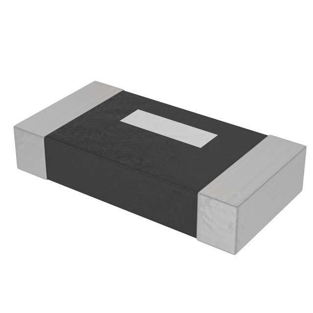
| 描述 | IC EEPROM 256KBIT 1MHZ 8SOIJ电可擦除可编程只读存储器 32kx8 - 2.5V Hi Spd |
| 产品分类 | |
| 品牌 | Microchip Technology |
| 产品手册 | |
| 产品图片 |
|
| rohs | 符合RoHS无铅 / 符合限制有害物质指令(RoHS)规范要求 |
| 产品系列 | 内存,电可擦除可编程只读存储器,Microchip Technology 24FC256-I/SM- |
| 数据手册 | http://www.microchip.com/mymicrochip/filehandler.aspx?ddocname=en011849 |
| 产品型号 | 24FC256-I/SM |
| PCN组件/产地 | |
| PCN设计/规格 | http://www.microchip.com/mymicrochip/NotificationDetails.aspx?id=5673&print=view |
| 产品培训模块 | http://www.digikey.cn/PTM/IndividualPTM.page?site=cn&lang=zhs&ptm=4315 |
| 产品目录页面 | |
| 产品种类 | 电可擦除可编程只读存储器 |
| 供应商器件封装 | 8-SOIJ |
| 其它名称 | 24FC256ISM |
| 包装 | 管件 |
| 商标 | Microchip Technology |
| 存储器类型 | EEPROM |
| 存储容量 | 256K (32K x 8) |
| 安装风格 | SMD/SMT |
| 封装 | Tube |
| 封装/外壳 | 8-SOIC(0.209",5.30mm 宽) |
| 封装/箱体 | SOIC-8 |
| 工作温度 | -40°C ~ 85°C |
| 工作电流 | 3 mA |
| 工作电源电压 | 1.8 V, 5.5 V |
| 工厂包装数量 | 90 |
| 接口 | I²C,2 线串口 |
| 接口类型 | I2C |
| 数据保留 | 200 yr |
| 最大工作温度 | + 85 C |
| 最大工作电流 | 3 mA |
| 最大时钟频率 | 1 MHz |
| 最小工作温度 | - 40 C |
| 标准包装 | 90 |
| 格式-存储器 | EEPROMs - 串行 |
| 电压-电源 | 1.7 V ~ 5.5 V |
| 电源电压-最大 | 5.5 V |
| 电源电压-最小 | 1.8 V |
| 组织 | 32 k x 8 |
| 访问时间 | 400 ns |
| 速度 | 400kHz,1MHz |


- 商务部:美国ITC正式对集成电路等产品启动337调查
- 曝三星4nm工艺存在良率问题 高通将骁龙8 Gen1或转产台积电
- 太阳诱电将投资9.5亿元在常州建新厂生产MLCC 预计2023年完工
- 英特尔发布欧洲新工厂建设计划 深化IDM 2.0 战略
- 台积电先进制程称霸业界 有大客户加持明年业绩稳了
- 达到5530亿美元!SIA预计今年全球半导体销售额将创下新高
- 英特尔拟将自动驾驶子公司Mobileye上市 估值或超500亿美元
- 三星加码芯片和SET,合并消费电子和移动部门,撤换高东真等 CEO
- 三星电子宣布重大人事变动 还合并消费电子和移动部门
- 海关总署:前11个月进口集成电路产品价值2.52万亿元 增长14.8%


PDF Datasheet 数据手册内容提取
24AA256/24LC256/24FC256 2 256K I C Serial EEPROM Device Selection Table Part Number VCC Range Max. Clock Frequency Temp. Ranges Available Packages 24AA256 1.7V-5.5V 400kHz(1) I, E MF, MS, P, SN, SM, MNY, ST, CS 24LC256 2.5V-5.5V 400kHz I, E MF, MS, P, SN, SM, MNY, ST 24FC256 1.7V-5.5V 1MHz(2) I MF, MS, P, SN, SM, MNY, ST Note 1: 100kHz for VCC<2.5V. 2: 400kHz for VCC<2.5V. Features Packages • Single Supply with Operation Down to 1.7V for • 8-Lead DFN, 8-Lead MSOP, 8-Lead PDIP, 24AA256 and 24FC256 Devices, 2.5V for 8-Lead SOIC, 8-Lead SOIJ, 8-Lead TDFN, 24LC256 Devices 8-Lead TSSOP and 8-Ball CSP • Low-Power CMOS Technology: Description - Write current: 3mA, maximum The Microchip Technology Inc. 24XX256(1) is a 32Kx8 - Standby current: 1µA maximum (I-temp.) • Two-Wire Serial Interface, I2C Compatible (256Kbit) Serial Electrically Erasable PROM, capable of operation across a broad voltage range (1.7V to • Cascadable up to Eight Devices 5.5V). It has been developed for advanced, low-power • Schmitt Trigger Inputs for Noise Suppression applications such as personal communications or data • Output Slope Control to Eliminate Ground Bounce acquisition. This device also has a page write capability • 100 kHz, 400 kHz and 1MHz Compatibility of up to 64bytes of data. This device is capable of both random and sequential reads up to the 256K boundary. • Page Write Time: 5ms, maximum Functional address lines allow up to eight devices on • Self-Timed Erase/Write Cycle the same bus, for up to 2Mbit address space. • 64-Byte Page Write Buffer • Hardware Write-Protect Note1: 24XX256 is used in this document as a • ESD Protection >4000V generic part number for the 24AA256/ • More than One Million Erase/Write Cycles 24LC256/24FC256 devices. • Data Retention >200 years • Factory Programming Available • RoHS Compliant • Temperature Ranges: - Industrial (I): -40C to +85C - Extended (E): -40C to +125C • Automotive AEC-Q100 Qualified Package Types 8-Lead DFN/TDFN 8-Lead PDIP/MSOP(1) 8-Lead SOIC/SOIJ/TSSOP 8-Ball CSP (Top View) (Top View) (Top View) (Top View) A0 1 8 VCC A0 11 88 VCC A0 1 8 VCC VCC A1 A0 A1 2 256 7 WP A1 22 56 77 WP A1 2 56 7 WP 1 2 3 VAS2S 34 24XX 65 SSCDLA VAS2S 3434 24XX2 6565 SSCDLA VAS2S 34 24XX2 65 SSCDLA WP 64 75 8 A2 SDA SCL VSS Note 1: Pins A0 and A1 are no connects for the MSOP package only. 1998-2019 Microchip Technology Inc. DS20001203W-page 1
24AA256/24LC256/24FC256 Block Diagram A0A1A2WP HV Generator I/O Memory EEPROM Control Control XDEC Array Logic Logic Page Latches I/O SCL YDEC SDA VCC VSS Sense Amp. R/W Control DS20001203W-page 2 1998-2019 Microchip Technology Inc.
24AA256/24LC256/24FC256 1.0 ELECTRICAL CHARACTERISTICS Absolute Maximum Ratings(†) VCC.............................................................................................................................................................................6.5V All inputs and outputs w.r.t. VSS..........................................................................................................-0.6V to VCC +1.0V Storage temperature...............................................................................................................................-65°C to +150°C Ambient temperature with power applied................................................................................................-40°C to +125°C ESD protection on all pins4kV † NOTICE: Stresses above those listed under “Absolute Maximum Ratings” may cause permanent damage to the device. This is a stress rating only and functional operation of the device at these or any other conditions above those indicated in the operational listings of this specification is not implied. Exposure to Absolute Maximum Rating conditions for extended periods may affect device reliability. TABLE 1-1: DC CHARACTERISTICS Electrical Characteristics: DC CHARACTERISTICS Industrial (I): VCC = +1.7V to 5.5V TA = -40°C to +85°C Extended (E): VCC = +1.7V to 5.5V TA = -40°C to +125°C Param. Symbol Characteristic Min. Max. Units Conditions No. D1 VIH High-Level Input Voltage 0.7 VCC — V D2 VIL Low-Level Input Voltage — 0.3 VCC V VCC 2.5V 0.2 VCC V VCC < 2.5V D3 VHYS Hysteresis of Schmitt Trigger 0.05 VCC — V VCC 2.5V (Note) Inputs (SDA, SCL pins) D4 VOL Low-Level Output Voltage — 0.40 V IOL = 3.0mA @ VCC = 4.5V IOL = 2.1mA @ VCC = 2.5V D5 ILI Input Leakage Current — ±1 µA VIN = VSS or VCC, WP = VSS VIN = VSS or VCC, WP = VCC D6 ILO Output Leakage Current — ±1 µA VOUT = VSS or VCC D7 CIN, Pin Capacitance — 10 pF VCC = 5.0V (Note) COUT (all inputs/outputs) TA = 25°C, FCLK = 1MHz D8 ICC Read Operating Current — 400 µA VCC = 5.5V, SCL = 400kHz ICC Write — 3 mA VCC = 5.5V D9 ICCS Standby Current — 1 µA SDA=SCL=VCC=3.6V A0, A1, A2, WP = VSS, I-Temp. — 1.5 µA SDA=SCL=VCC=5.5V A0, A1, A2, WP = VSS, I-Temp. — 5 µA SDA=SCL=VCC=5.5V A0, A1, A2, WP = VSS, E-Temp. Note: This parameter is periodically sampled and not 100% tested. 1998-2019 Microchip Technology Inc. DS20001203W-page 3
24AA256/24LC256/24FC256 TABLE 1-2: AC CHARACTERISTICS Electrical Characteristics: AC CHARACTERISTICS Industrial (I): VCC = +1.7V to 5.5V TA = -40°C to +85°C Extended (E): VCC = +1.7V to 5.5V TA = -40°C to +125°C Param. Symbol Characteristic Min. Max. Units Conditions No. 1 FCLK Clock Frequency — 100 kHz 1.7V VCC 2.5V — 400 kHz 2.5V VCC 5.5V — 400 kHz 1.7V VCC 2.5V (24FC256) — 1000 kHz 2.5V VCC 5.5V (24FC256) 2 THIGH Clock High Time 4000 — ns 1.7V VCC 2.5V 600 — ns 2.5V VCC 5.5V 600 — ns 1.7V VCC 2.5V (24FC256) 500 — ns 2.5V VCC 5.5V (24FC256) 3 TLOW Clock Low Time 4700 — ns 1.7V VCC 2.5V 1300 — ns 2.5V VCC 5.5V 1300 — ns 1.7V VCC 2.5V (24FC256) 500 — ns 2.5V VCC 5.5V (24FC256) 4 TR SDA and SCL Rise Time — 1000 ns 1.7V VCC 2.5V (Note1) — 300 ns 2.5V VCC 5.5V (Note1) — 300 ns 1.7V VCC 5.5V (24FC256) (Note1) 5 TF SDA and SCL Fall Time — 300 ns All except 24FC256 (Note1) — 100 ns 1.7V VCC 5.5V (24FC256) (Note1) 6 THD:STA Start Condition Hold Time 4000 — ns 1.7V VCC 2.5V 600 — ns 2.5V VCC 5.5V 600 — ns 1.7V VCC 2.5V (24FC256) 250 — ns 2.5V VCC 5.5V (24FC256) 7 TSU:STA Start Condition Setup Time 4700 — ns 1.7V VCC 2.5V 600 — ns 2.5V VCC 5.5V 600 — ns 1.7V VCC 2.5V (24FC256) 250 — ns 2.5V VCC 5.5V (24FC256) 8 THD:DAT Data Input Hold Time 0 — ns Note2 9 TSU:DAT Data Input Setup Time 250 — ns 1.7V VCC 2.5V 100 — ns 2.5V VCC 5.5V 100 — ns 1.7V VCC 5.5V (24FC256) 10 TSU:STO Stop Condition Setup Time 4000 — ns 1.7V VCC 2.5V 600 — ns 2.5V VCC 5.5V 600 — ns 1.7V VCC 2.5V (24FC256) 250 — ns 2.5V VCC 5.5V (24FC256) Note 1: Not 100% tested. CB = total capacitance of one bus line in pF. 2: As a transmitter, the device must provide an internal minimum delay time to bridge the undefined region (minimum 300ns) of the falling edge of SCL to avoid unintended generation of Start or Stop conditions. 3: The combined TSP and VHYS specifications are due to new Schmitt Trigger inputs, which provide improved noise spike suppression. This eliminates the need for a TI specification for standard operation. 4: This parameter is not tested but ensured by characterization. For endurance estimates in a specific application, please consult the Total Endurance™ Model, which can be obtained from Microchip’s website at www.microchip.com. DS20001203W-page 4 1998-2019 Microchip Technology Inc.
24AA256/24LC256/24FC256 TABLE 1-2: AC CHARACTERISTICS Electrical Characteristics: AC CHARACTERISTICS (Continued) Industrial (I): VCC = +1.7V to 5.5V TA = -40°C to +85°C Extended (E): VCC = +1.7V to 5.5V TA = -40°C to +125°C Param. Symbol Characteristic Min. Max. Units Conditions No. 11 TSU:WP WP Setup Time 4000 — ns 1.7V VCC 2.5V 600 — ns 2.5V VCC 5.5V 600 — ns 1.7V VCC 5.5V (24FC256) 12 THD:WP WP Hold Time 4700 — ns 1.7V VCC 2.5V 1300 — ns 2.5V VCC 5.5V 1300 — ns 1.7V VCC 5.5V (24FC256) 13 TAA Output Valid from Clock — 3500 ns 1.7V VCC 2.5V (Note2) — 900 ns 2.5V VCC 5.5V (Note2) — 900 ns 1.7V VCC 2.5V (24FC256) (Note2) — 400 ns 2.5V VCC 5.5V (24FC256) (Note2) 14 TBUF Bus Free Time: The time the 4700 — ns 1.7V VCC 2.5V bus must be free before a new 1300 — ns 2.5V VCC 5.5V transmission can start 1300 — ns 1.7V VCC 2.5V (24FC256) 500 — ns 2.5V VCC 5.5V (24FC256) 15 TOF Output fall time from VIH 10 + 0.1CB 250 ns All except 24FC256 (Note1) minimum to VIL maximum 250 ns All except 24FC256 (Note1) CB 100pF 16 TSP Input Filter Spike Suppression — 50 ns All except 24FC256 (SDA and SCL pins) (Notes1 and3) 17 TWC Write Cycle Time — 5 ms (byte or page) 18 Endurance 1,000,000 — cycles 25°C, 5.5V, Page mode (Note4) Note 1: Not 100% tested. CB = total capacitance of one bus line in pF. 2: As a transmitter, the device must provide an internal minimum delay time to bridge the undefined region (minimum 300ns) of the falling edge of SCL to avoid unintended generation of Start or Stop conditions. 3: The combined TSP and VHYS specifications are due to new Schmitt Trigger inputs, which provide improved noise spike suppression. This eliminates the need for a TI specification for standard operation. 4: This parameter is not tested but ensured by characterization. For endurance estimates in a specific application, please consult the Total Endurance™ Model, which can be obtained from Microchip’s website at www.microchip.com. 1998-2019 Microchip Technology Inc. DS20001203W-page 5
24AA256/24LC256/24FC256 FIGURE 1-1: BUS TIMING DATA 5 4 2 D3 SCL 7 3 8 9 10 SDA 6 IN 16 13 14 SDA OUT (protected) WP 11 12 (unprotected) DS20001203W-page 6 1998-2019 Microchip Technology Inc.
24AA256/24LC256/24FC256 2.0 PIN DESCRIPTIONS The descriptions of the pins are listed in Table2-1. TABLE 2-1: PIN FUNCTION TABLE Name DFN(1) MSOP PDIP SOIC SOIJ TDFN(1) TSSOP CSP Function A0 1 — 1 1 1 1 1 3 User Configurable Chip Select A1 2 — 2 2 2 2 2 2 User Configurable Chip Select A2 3 3 3 3 3 3 3 5 User Configurable Chip Select VSS 4 4 4 4 4 4 4 8 Ground SDA 5 5 5 5 5 5 5 6 Serial Address/Data I/O SCL 6 6 6 6 6 6 6 7 Serial Clock WP 7 7 7 7 7 7 7 4 Write-Protect Input VCC 8 8 8 8 8 8 8 1 Power Supply Note1: Exposed pad on DFN/TDFN can be connected to VSS or left floating. 2.1 A0, A1, A2 Chip Address Inputs 2.3 Serial Clock (SCL) The A0, A1 and A2 inputs are used by the 24XX256 for This input is used to synchronize the data transfer to multiple device operations. The levels on these inputs and from the device. are compared with the corresponding bits in the slave address. The chip is selected if the compare is true. 2.4 Write-Protect (WP) Note: For the MSOP package only, pins A0 and This pin must be connected to either VSS or VCC. If tied A1 are not connected. to VSS, write operations are enabled. If tied to VCC, write operations are inhibited but read operations are Up to eight devices (two for the MSOP package) may not affected. be connected to the same bus by using different Chip Select bit combinations. These inputs must be connected to either VCC or VSS. In most applications, the chip address inputs A0, A1 and A2 are hard-wired to logic ‘0’ or logic ‘1’. For applications in which these pins are controlled by a microcontroller or other programmable device, the chip address pins must be driven to logic ‘0’ or logic ‘1’ before normal device operation can proceed. 2.2 Serial Data (SDA) This is a bidirectional pin used to transfer addresses and data into and out of the device. It is an open-drain terminal. Therefore, the SDA bus requires a pull-up resistor to VCC (typical 10k for 100kHz, 2kfor 400kHz and 1MHz). For normal data transfer, SDA is allowed to change only during SCL low. Changes during SCL high are reserved for indicating the Start and Stop conditions. 1998-2019 Microchip Technology Inc. DS20001203W-page 7
24AA256/24LC256/24FC256 3.0 FUNCTIONAL DESCRIPTION 4.4 Data Valid (D) The 24XX256 supports a bidirectional two-wire bus and The state of the data line represents valid data when, data transmission protocol. A device that sends data after a Start condition, the data line is stable for the onto the bus is defined as a transmitter and a device duration of the high period of the clock signal. receiving data as a receiver. The bus must be The data on the line must be changed during the low controlled by a master device which generates the period of the clock signal. There is one bit of data per Serial Clock (SCL), controls the bus access, and clock pulse. generates the Start and Stop conditions while the Each data transfer is initiated with a Start condition and 24XX256 works as a slave. Both master and slave can terminated with a Stop condition. The number of the operate as a transmitter or receiver, but the master data bytes transferred between the Start and Stop device determines which mode is activated. conditions is determined by the master device and is, theoretically, unlimited (although only the last 64 will be 4.0 BUS CHARACTERISTICS stored when doing a write operation). When an over- write does occur it will replace data in a first-in-first-out The following bus protocol has been defined: (FIFO) principle. • Data transfer may be initiated only when the bus is not busy. 4.5 Acknowledge • During data transfer, the data line must remain stable whenever the clock line is high. Changes in Each receiving device, when addressed, is obliged to the data line, while the clock line is high, will be generate an Acknowledge signal after the reception of interpreted as a Start or Stop condition. each byte. The master device must generate an extra clock pulse which is associated with this Acknowledge Accordingly, the following bus conditions have been bit. defined (Figure4-1). Note: The 24XX256 does not generate any 4.1 Bus Not Busy (A) Acknowledge bits if an internal programming cycle is in progress. Both data and clock lines remain high. A device that acknowledges must pull down the SDA line during the Acknowledge clock pulse in such a way 4.2 Start Data Transfer (B) that the SDA line is stable-low during the high period of A high-to-low transition of the SDA line while the clock the Acknowledge-related clock pulse. Moreover, setup (SCL) is high, determines a Start condition. All and hold times must be taken into account. During commands must be preceded by a Start condition. reads, a master must signal an end of data to the slave by NOT generating an Acknowledge bit on the last byte 4.3 Stop Data Transfer (C) that has been clocked out of the slave. In this case, the slave (24XX256) will leave the data line high to enable A low-to-high transition of the SDA line, while the clock the master to generate the Stop condition. (SCL) is high, determines a Stop condition. All operations must end with a Stop condition. DS20001203W-page 8 1998-2019 Microchip Technology Inc.
24AA256/24LC256/24FC256 FIGURE 4-1: DATA TRANSFER SEQUENCE ON THE SERIAL BUS (A) (B) (D) (D) (C) (A) SCL SDA Start Address or Data Stop Condition Acknowledge Allowed Condition Valid to Change FIGURE 4-2: ACKNOWLEDGE TIMING Acknowledge Bit SCL 1 2 3 4 5 6 7 8 9 1 2 3 SDA Data from transmitter Data from transmitter Transmitter must release the SDA line at this point, Receiver must release the SDA line allowing the Receiver to pull the SDA line low to at this point so the Transmitter can acknowledge the previous eight bits of data. continue sending data. 1998-2019 Microchip Technology Inc. DS20001203W-page 9
24AA256/24LC256/24FC256 5.0 DEVICE ADDRESSING FIGURE 5-1: CONTROL BYTE FORMAT A control byte is the first byte received following the Start condition from the master device. The control byte Read/Write Bit consists of a 4-bit control code. For the 24XX256, this is set as ‘1010’ binary for read and write operations. Chip Select The next three bits of the control byte are the Chip Control Code Bits Select bits (A2, A1, A0). The Chip Select bits allow the use of up to eight 24XX256 devices on the same bus S 1 0 1 0 A2 A1 A0 R/W ACK and are used to select which device is accessed. The Chip Select bits in the control byte must correspond to Slave Address the logic levels on the corresponding A2, A1 and A0 pins for the device to respond. These bits, in effect, are Start Bit Acknowledge Bit the three Most Significant bits of the word address. The combination of the 4-bit control code and the next three bits are called the slave address. 5.1 Contiguous Addressing Across For the MSOP package, the A0 and A1 pins are not Multiple Devices connected. During device addressing, the A0 and A1 Chip Select bits (Figures5-1 and 5-2) should be set The Chip Select bits A2, A1 and A0 can be used to to‘0’. Only two 24XX256 MSOP packages can be expand the contiguous address space for up to 2Mbit connected to the same bus. by adding up to eight 24XX256 devices on the same bus. In this case, software can use A0 of the control The last bit of the control byte is the Read/Write (R/W) byte as address bit A15; A1 as address bit A16; and A2 bit and it defines the operation to be performed. When as address bit A17. It is not possible to sequentially set to ‘1’, a read operation is selected. When set to ‘0’, read across device boundaries. a write operation is selected. The next two bytes received define the address of the first data byte For the MSOP package, up to two 24XX256 devices (Figure5-2). Because only A14…A0 are used, the can be added for up to 512Kbit of address space. In upper address bits are a “don’t care.” The upper this case, software can use A2 of the control byte as address bits are transferred first, followed by the Least address bit A17. Bits A0 (A15) and A1 (A16) of the Significant bits. control byte must always be set to a logic ‘0’ for the MSOP. Following the Start condition, the 24XX256 monitors the SDA bus checking the device type identifier being transmitted. Upon receiving a ‘1010’ code and appropriate device select bits, the slave device outputs an Acknowledge signal on the SDA line. Depending on the state of the R/W bit, the 24XX256 will select a read or write operation. FIGURE 5-2: ADDRESS SEQUENCE BIT ASSIGNMENTS Control Byte Address High Byte Address Low Byte A A A A A A A A A A A A 1 0 1 0 2 1 0 R/W x 14 13 12 11 10 9 8 7 • • • • • • 0 Control Chip Code Select Bits x = “don’t care” bit DS20001203W-page 10 1998-2019 Microchip Technology Inc.
24AA256/24LC256/24FC256 6.0 WRITE OPERATIONS Note: Page write operations are limited to writing bytes within a single physical page, 6.1 Byte Write regardless of the number of bytes actually being written. Physical page Following the Start condition from the master, the boundaries start at addresses that are control code (four bits), the Chip Select (three bits) and integer multiples of the page buffer size the R/W bit (which is a logic low) are clocked onto the (or ‘page size’) and end at addresses that bus by the master transmitter. This indicates to the are integer multiples of page size – 1. If a addressed slave receiver that the address high byte will page write command attempts to write follow after it has generated an Acknowledge bit during across a physical page boundary, the the ninth clock cycle. Therefore, the next byte result is that the data wraps around to the transmitted by the master is the high-order byte of the beginning of the current page (overwriting word address and will be written into the Address data previously stored there), instead of Pointer of the 24XX256. The next byte is the Least being written to the next page, as might be Significant Address Byte. After receiving another expected. It is, therefore, necessary for Acknowledge signal from the 24XX256, the master the application software to prevent page device will transmit the data word to be written into the write operations that would attempt to addressed memory location. The 24XX256 acknowl- cross a page boundary. edges again and the master generates a Stop condition. This initiates the internal write cycle and 6.3 Write Protection during this time, the 24XX256 will not generate Acknowledge signals (Figure6-1). If an attempt is The WP pin allows the user to write-protect the entire made to write to the array with the WP pin held high, the array (0000-7FFF) when the pin is tied to VCC. If tied to device will acknowledge the command but no write VSS the write protection is disabled. The WP pin is cycle will occur, no data will be written, and the device sampled at the Stop bit for every write command will immediately accept a new command. After a byte (Figure1-1). Toggling the WP pin after the Stop bit will write command, the internal address counter will point have no effect on the execution of the write cycle. to the address location following the one that was just written. Note: When doing a write of less than 64 bytes, the data in the rest of the page is refreshed along with the data bytes being written. This will force the entire page to endure a write cycle, for this reason endurance is specified per page. 6.2 Page Write The write control byte, word address and the first data byte are transmitted to the 24XX256 in much the same way as in a byte write. The exception is that instead of generating a Stop condition, the master transmits up to 63 additional bytes, which are temporarily stored in the on-chip page buffer, and will be written into memory once the master has transmitted a Stop condition. Upon receipt of each word, the six lower Address Pointer bits, which form the byte counter, are internally incremented by one. If the master should transmit more than 64 bytes prior to generating the Stop condition, the address counter will roll over and the previously received data will be overwritten. As with the byte write operation, once the Stop condition is received, an inter- nal write cycle will begin (Figure6-2). If an attempt is made to write to the array with the WP pin held high, the device will acknowledge the command, but no write cycle will occur, no data will be written and the device will immediately accept a new command. 1998-2019 Microchip Technology Inc. DS20001203W-page 11
24AA256/24LC256/24FC256 FIGURE 6-1: BYTE WRITE S Bus Activity T S Control Address Address Master A T R Byte High Byte Low Byte Data O SDA Line T P AAA S1 0 1 0 2 10 0 x P Bus Activity A A A A x = “don’t care” bit C C C C K K K K FIGURE 6-2: PAGE WRITE S Bus Activity T S Master A Control Address Address T R Byte High Byte Low Byte Data Byte 0 Data Byte 63 O T P SDA Line AAA S10 1 0 2 1 0 0 x P Bus Activity A A A A A C C C C C x = “don’t care” bit K K K K K 7.0 ACKNOWLEDGE POLLING FIGURE 7-1: ACKNOWLEDGE POLLING FLOW Since the device will not acknowledge during a write cycle, this can be used to determine when the cycle is complete (This feature can be used to maximize bus throughput). Once the Stop condition for a write Send command has been issued from the master, the device Write Command initiates the internally timed write cycle. ACK polling can be initiated immediately. This involves the master sending a Start condition, followed by the control byte Send Stop for a write command (R/W=0). If the device is still Condition to busy with the write cycle, then no ACK will be returned. Initiate Write Cycle If no ACK is returned, the Start bit and control byte must be resent. If the cycle is complete, then the device will return the ACK and the master can then proceed with the next read or write command. See Figure7-1 for Send Start flow diagram. Send Control Byte with R/W = 0 Did Device NO Acknowledge (ACK = 0)? YES Next Operation DS20001203W-page 12 1998-2019 Microchip Technology Inc.
24AA256/24LC256/24FC256 8.0 READ OPERATION 8.2 Random Read Read operations are initiated in much the same way as Random read operations allow the master to access write operations, with the exception that the R/W bit of any memory location in a random manner. To perform the control byte is set to ‘1’. There are three basic types this type of read operation, the word address must first of read operations: current address read, random read be set. This is done by sending the word address to the and sequential read. 24XX256 as part of a write operation (R/W bit set to‘0’). Once the word address is sent, the master gen- 8.1 Current Address Read erates a Start condition following the Acknowledge. This terminates the write operation, but not before the The 24XX256 contains an address counter that main- internal Address Pointer is set. The master then issues tains the address of the last word accessed, internally the control byte again, but with the R/W bit set to a one. incremented by one. Therefore, if the previous read The 24XX256 will then issue an Acknowledge and access was to address n (n is any legal address), the transmit the 8-bit data word. The master will not next current address read operation would access data acknowledge the transfer, though it does generate a from address n + 1. Stop condition, which causes the 24XX256 to discon- Upon receipt of the control byte with R/W bit set to ‘1’, tinue transmission (Figure8-2). After a random read the 24XX256 issues an Acknowledge and transmits the command, the internal address counter will point to the 8-bit data word. The master will not acknowledge the address location following the one that was just read. transfer, but does generate a Stop condition and the 24XX256 discontinues transmission (Figure8-1). 8.3 Sequential Read Sequential reads are initiated in the same way as a FIGURE 8-1: CURRENT ADDRESS random read except that after the 24XX256 transmits READ the first data byte, the master issues an Acknowledge S (as opposed to the Stop condition used in a random Bus Activity TA Control Data ST read). This Acknowledge directs the 24XX256 to Master R Byte Byte O transmit the next sequentially addressed 8-bit word T P (Figure8-3). Following the final byte transmitted to the SDA Line S 1 0 1 0 AAA 1 P master, the master will NOT generate an Acknowledge, 2 1 0 A N but will generate a Stop condition. Bus Activity C O K To provide sequential reads, the 24XX256 contains an A internal Address Pointer which is incremented by one C K at the completion of each operation. This Address Pointer allows the entire memory contents to be serially read during one operation. The internal Address Pointer will automatically roll over from address 7FFF to address 0000 if the master acknowledges the byte received from the array address 7FFF. FIGURE 8-2: RANDOM READ S S Bus Activity T T S Control Address Address Control Data Master A A T R Byte High Byte Low Byte R Byte Byte O T T P SDA Line S1 0 1 0 AAA0 x S1 0 1 0 AAA1 P 2 1 0 2 1 0 A A A A N Bus Activity C C C C O K K K K A x = “don’t care” bit C K 1998-2019 Microchip Technology Inc. DS20001203W-page 13
24AA256/24LC256/24FC256 FIGURE 8-3: SEQUENTIAL READ Control S Bus Activity T Master Byte Data (n) Data (n + 1) Data (n + 2) Data (n + x) O P SDA Line P A A A A N C C C C O Bus Activity K K K K A C K DS20001203W-page 14 1998-2019 Microchip Technology Inc.
24AA256/24LC256/24FC256 9.0 PACKAGING INFORMATION 9.1 Package Marking Information 8-Lead DFN-S Example XXXXXXX 24LC256 XXXXXXX I/MF e3 YYWW 1926 13F NNN 8-Lead MSOP Example XXXXXX 4L256I YWWNNN 92613F 8-Lead PDIP (300 mil) Example XXXXXXXX 24AA256 XXXXXNNN I/P e 3 13F YYWW 1926 8-Lead SOIC (3.90 mm) Example XXXXXXXX 24LC256I XXXXYYWW SN e 3 1926 NNN 13F 8-Lead SOIJ (5.28 mm) Example XXXXXXXX 24LC256 XXXXXXXX I/SM e3 YYWWNNN 192613F 1998-2019 Microchip Technology Inc. DS20001203W-page 15
24AA256/24LC256/24FC256 Package Marking Information (Continued) 8-Lead TDFN Example XXX EF4 YWW 1926 NN 13 8-Lead TSSOP Example XXXX 4LD XYWW I926 NNN 13F 8-Lead Chip Scale Example XXX 249 XYYW A192 WNNN 613F 1st Line Marking Codes Part TDFN No. DFN MSOP PDIP SOIC SOIJ TSSOP CSP I-Temp. E-Temp. 24AA256 24AA256 4A256T(1) 24AA256 24AA256T(1) 24AA256 EF6 EF5 4AD 249 24LC256 24LC256 4L256T(1) 24LC256 24LC256T(1) 24LC256 EF4 EF3 4LD — 24FC256 24FC256 4F256T(1) 24FC256 24FC256T(1) 24FC256 EF8 — 4FD — Note 1: T = Temperature grade (I, E) Legend: XX...X Part number or part number code T Temperature (I, E) Y Year code (last digit of calendar year) YY Year code (last 2 digits of calendar year) WW Week code (week of January 1 is week ‘01’) NNN Alphanumeric traceability code (2 characters for small packages) e3 JEDEC® designator for Matte Tin (Sn) * Standard OTP marking consists of Microchip part number, year code, week code and traceability code. Note: For very small packages with no room for the JEDEC® designator e 3 , the marking will only appear on the outer carton or reel label. Note: In the event the full Microchip part number cannot be marked on one line, it will be carried over to the next line, thus limiting the number of available characters for customer-specific information. DS20001203W-page 16 1998-2019 Microchip Technology Inc.
24AA256/24LC256/24FC256 (cid:2)(cid:3)(cid:4)(cid:5)(cid:6)(cid:7)(cid:8)(cid:9)(cid:10)(cid:6)(cid:11)(cid:12)(cid:13)(cid:14)(cid:8)(cid:15)(cid:16)(cid:6)(cid:10)(cid:8)(cid:17)(cid:10)(cid:6)(cid:12)(cid:18)(cid:8)(cid:19)(cid:20)(cid:8)(cid:4)(cid:5)(cid:6)(cid:7)(cid:8)(cid:9)(cid:6)(cid:14)(cid:21)(cid:6)(cid:22)(cid:5)(cid:8)(cid:23)(cid:24)(cid:17)(cid:25)(cid:8)(cid:26)(cid:8)(cid:27)(cid:28)(cid:29)(cid:8)(cid:30)(cid:30)(cid:8)(cid:31)(cid:20)(cid:7) (cid:8)!(cid:15)(cid:17)(cid:19)(cid:3)"# (cid:19)(cid:20)(cid:12)(cid:5)$ 3(cid:22)(cid:21)(cid:14)&(cid:23)(cid:13)(cid:14)’(cid:22)!&(cid:14)(cid:20)"(cid:21)(cid:21)(cid:13)(cid:25)&(cid:14)(cid:10)(cid:11)(cid:20)+(cid:11)(cid:12)(cid:13)(cid:14)#(cid:21)(cid:11)*(cid:19)(cid:25)(cid:12)!((cid:14)(cid:10)(cid:26)(cid:13)(cid:11)!(cid:13)(cid:14)!(cid:13)(cid:13)(cid:14)&(cid:23)(cid:13)(cid:14)(cid:18)(cid:19)(cid:20)(cid:21)(cid:22)(cid:20)(cid:23)(cid:19)(cid:10)(cid:14)(cid:31)(cid:11)(cid:20)+(cid:11)(cid:12)(cid:19)(cid:25)(cid:12)(cid:14)(cid:3)(cid:10)(cid:13)(cid:20)(cid:19)%(cid:19)(cid:20)(cid:11)&(cid:19)(cid:22)(cid:25)(cid:14)(cid:26)(cid:22)(cid:20)(cid:11)&(cid:13)#(cid:14)(cid:11)&(cid:14) (cid:23)&&(cid:10)244***(cid:29)’(cid:19)(cid:20)(cid:21)(cid:22)(cid:20)(cid:23)(cid:19)(cid:10)(cid:29)(cid:20)(cid:22)’4(cid:10)(cid:11)(cid:20)+(cid:11)(cid:12)(cid:19)(cid:25)(cid:12) (cid:14) e D L b N N K E E2 EXPOSEDPAD NOTE1 NOTE1 1 2 2 1 D2 TOPVIEW BOTTOMVIEW A A3 A1 NOTE2 5(cid:25)(cid:19)&! (cid:18)(cid:28)66(cid:28)(cid:18)-(cid:24)-(cid:8)(cid:3) (cid:2)(cid:19)’(cid:13)(cid:25)!(cid:19)(cid:22)(cid:25)(cid:14)6(cid:19)’(cid:19)&! (cid:18)(cid:28)7 78(cid:18) (cid:18)(cid:7)9 7"’)(cid:13)(cid:21)(cid:14)(cid:22)%(cid:14)(cid:31)(cid:19)(cid:25)! 7 : (cid:31)(cid:19)&(cid:20)(cid:23) (cid:13) (cid:30)(cid:29)(cid:16)(cid:17)(cid:14)0(cid:3)1 8 (cid:13)(cid:21)(cid:11)(cid:26)(cid:26)(cid:14);(cid:13)(cid:19)(cid:12)(cid:23)& (cid:7) (cid:4)(cid:29):(cid:4) (cid:4)(cid:29):/ (cid:30)(cid:29)(cid:4)(cid:4) (cid:3)&(cid:11)(cid:25)#(cid:22)%%(cid:14) (cid:7)(cid:30) (cid:4)(cid:29)(cid:4)(cid:4) (cid:4)(cid:29)(cid:4)(cid:30) (cid:4)(cid:29)(cid:4)/ 1(cid:22)(cid:25)&(cid:11)(cid:20)&(cid:14)(cid:24)(cid:23)(cid:19)(cid:20)+(cid:25)(cid:13)!! (cid:7), (cid:4)(cid:29)(cid:16)(cid:4)(cid:14)(cid:8)-3 8 (cid:13)(cid:21)(cid:11)(cid:26)(cid:26)(cid:14)6(cid:13)(cid:25)(cid:12)&(cid:23) (cid:2) /(cid:29)(cid:4)(cid:4)(cid:14)0(cid:3)1 8 (cid:13)(cid:21)(cid:11)(cid:26)(cid:26)(cid:14)<(cid:19)#&(cid:23) - (cid:15)(cid:29)(cid:4)(cid:4)(cid:14)0(cid:3)1 -$(cid:10)(cid:22)!(cid:13)#(cid:14)(cid:31)(cid:11)#(cid:14)6(cid:13)(cid:25)(cid:12)&(cid:23) (cid:2)(cid:16) ,(cid:29)(cid:6)(cid:4) (cid:5)(cid:29)(cid:4)(cid:4) (cid:5)(cid:29)(cid:30)(cid:4) -$(cid:10)(cid:22)!(cid:13)#(cid:14)(cid:31)(cid:11)#(cid:14)<(cid:19)#&(cid:23) -(cid:16) (cid:16)(cid:29)(cid:16)(cid:4) (cid:16)(cid:29),(cid:4) (cid:16)(cid:29)(cid:5)(cid:4) 1(cid:22)(cid:25)&(cid:11)(cid:20)&(cid:14)<(cid:19)#&(cid:23) ) (cid:4)(cid:29),/ (cid:4)(cid:29)(cid:5)(cid:4) (cid:4)(cid:29)(cid:5): 1(cid:22)(cid:25)&(cid:11)(cid:20)&(cid:14)6(cid:13)(cid:25)(cid:12)&(cid:23) 6 (cid:4)(cid:29)/(cid:4) (cid:4)(cid:29)(cid:15)(cid:4) (cid:4)(cid:29)(cid:17)/ 1(cid:22)(cid:25)&(cid:11)(cid:20)&(cid:9)&(cid:22)(cid:9)-$(cid:10)(cid:22)!(cid:13)#(cid:14)(cid:31)(cid:11)# = (cid:4)(cid:29)(cid:16)(cid:4) > > (cid:19)(cid:20)(cid:12)(cid:5)(cid:11)$ (cid:30)(cid:29) (cid:31)(cid:19)(cid:25)(cid:14)(cid:30)(cid:14) (cid:19)!"(cid:11)(cid:26)(cid:14)(cid:19)(cid:25)#(cid:13)$(cid:14)%(cid:13)(cid:11)&"(cid:21)(cid:13)(cid:14)’(cid:11)(cid:27)(cid:14) (cid:11)(cid:21)(cid:27)((cid:14))"&(cid:14)’"!&(cid:14))(cid:13)(cid:14)(cid:26)(cid:22)(cid:20)(cid:11)&(cid:13)#(cid:14)*(cid:19)&(cid:23)(cid:19)(cid:25)(cid:14)&(cid:23)(cid:13)(cid:14)(cid:23)(cid:11)&(cid:20)(cid:23)(cid:13)#(cid:14)(cid:11)(cid:21)(cid:13)(cid:11)(cid:29) (cid:16)(cid:29) (cid:31)(cid:11)(cid:20)+(cid:11)(cid:12)(cid:13)(cid:14)’(cid:11)(cid:27)(cid:14)(cid:23)(cid:11) (cid:13)(cid:14)(cid:22)(cid:25)(cid:13)(cid:14)(cid:22)(cid:21)(cid:14)’(cid:22)(cid:21)(cid:13)(cid:14)(cid:13)$(cid:10)(cid:22)!(cid:13)#(cid:14)&(cid:19)(cid:13)(cid:14))(cid:11)(cid:21)!(cid:14)(cid:11)&(cid:14)(cid:13)(cid:25)#!(cid:29) ,(cid:29) (cid:31)(cid:11)(cid:20)+(cid:11)(cid:12)(cid:13)(cid:14)(cid:19)!(cid:14)!(cid:11)*(cid:14)!(cid:19)(cid:25)(cid:12)"(cid:26)(cid:11)&(cid:13)#(cid:29) (cid:5)(cid:29) (cid:2)(cid:19)’(cid:13)(cid:25)!(cid:19)(cid:22)(cid:25)(cid:19)(cid:25)(cid:12)(cid:14)(cid:11)(cid:25)#(cid:14)&(cid:22)(cid:26)(cid:13)(cid:21)(cid:11)(cid:25)(cid:20)(cid:19)(cid:25)(cid:12)(cid:14)(cid:10)(cid:13)(cid:21)(cid:14)(cid:7)(cid:3)(cid:18)-(cid:14).(cid:30)(cid:5)(cid:29)/(cid:18)(cid:29) 0(cid:3)12 0(cid:11)!(cid:19)(cid:20)(cid:14)(cid:2)(cid:19)’(cid:13)(cid:25)!(cid:19)(cid:22)(cid:25)(cid:29)(cid:14)(cid:24)(cid:23)(cid:13)(cid:22)(cid:21)(cid:13)&(cid:19)(cid:20)(cid:11)(cid:26)(cid:26)(cid:27)(cid:14)(cid:13)$(cid:11)(cid:20)&(cid:14) (cid:11)(cid:26)"(cid:13)(cid:14)!(cid:23)(cid:22)*(cid:25)(cid:14)*(cid:19)&(cid:23)(cid:22)"&(cid:14)&(cid:22)(cid:26)(cid:13)(cid:21)(cid:11)(cid:25)(cid:20)(cid:13)!(cid:29) (cid:8)-32 (cid:8)(cid:13)%(cid:13)(cid:21)(cid:13)(cid:25)(cid:20)(cid:13)(cid:14)(cid:2)(cid:19)’(cid:13)(cid:25)!(cid:19)(cid:22)(cid:25)((cid:14)"!"(cid:11)(cid:26)(cid:26)(cid:27)(cid:14)*(cid:19)&(cid:23)(cid:22)"&(cid:14)&(cid:22)(cid:26)(cid:13)(cid:21)(cid:11)(cid:25)(cid:20)(cid:13)((cid:14)%(cid:22)(cid:21)(cid:14)(cid:19)(cid:25)%(cid:22)(cid:21)’(cid:11)&(cid:19)(cid:22)(cid:25)(cid:14)(cid:10)"(cid:21)(cid:10)(cid:22)!(cid:13)!(cid:14)(cid:22)(cid:25)(cid:26)(cid:27)(cid:29) (cid:18)(cid:19)(cid:20)(cid:21)(cid:22)(cid:20)(cid:23)(cid:19)(cid:10)(cid:24)(cid:13)(cid:20)(cid:23)(cid:25)(cid:22)(cid:26)(cid:22)(cid:12)(cid:27)(cid:2)(cid:21)(cid:11)*(cid:19)(cid:25)(cid:12)1(cid:4)(cid:5)(cid:9)(cid:30)(cid:16)(cid:16)0 1998-2019 Microchip Technology Inc. DS20001203W-page 17
24AA256/24LC256/24FC256 (cid:19)(cid:20)(cid:12)(cid:5)$ 3(cid:22)(cid:21)(cid:14)&(cid:23)(cid:13)(cid:14)’(cid:22)!&(cid:14)(cid:20)"(cid:21)(cid:21)(cid:13)(cid:25)&(cid:14)(cid:10)(cid:11)(cid:20)+(cid:11)(cid:12)(cid:13)(cid:14)#(cid:21)(cid:11)*(cid:19)(cid:25)(cid:12)!((cid:14)(cid:10)(cid:26)(cid:13)(cid:11)!(cid:13)(cid:14)!(cid:13)(cid:13)(cid:14)&(cid:23)(cid:13)(cid:14)(cid:18)(cid:19)(cid:20)(cid:21)(cid:22)(cid:20)(cid:23)(cid:19)(cid:10)(cid:14)(cid:31)(cid:11)(cid:20)+(cid:11)(cid:12)(cid:19)(cid:25)(cid:12)(cid:14)(cid:3)(cid:10)(cid:13)(cid:20)(cid:19)%(cid:19)(cid:20)(cid:11)&(cid:19)(cid:22)(cid:25)(cid:14)(cid:26)(cid:22)(cid:20)(cid:11)&(cid:13)#(cid:14)(cid:11)&(cid:14) (cid:23)&&(cid:10)244***(cid:29)’(cid:19)(cid:20)(cid:21)(cid:22)(cid:20)(cid:23)(cid:19)(cid:10)(cid:29)(cid:20)(cid:22)’4(cid:10)(cid:11)(cid:20)+(cid:11)(cid:12)(cid:19)(cid:25)(cid:12) DS20001203W-page 18 1998-2019 Microchip Technology Inc.
24AA256/24LC256/24FC256 Note: For the mostcurrent package drawings,please seetheMicrochip Packaging Specification located at http://www.microchip.com/packaging 1998-2019 Microchip Technology Inc. DS20001203W-page 19
24AA256/24LC256/24FC256 Note: For the mostcurrent package drawings,please seetheMicrochip Packaging Specification located at http://www.microchip.com/packaging DS20001203W-page 20 1998-2019 Microchip Technology Inc.
24AA256/24LC256/24FC256 Note: For the most current package drawings, please see the Microchip Packaging Specification located at http://www.microchip.com/packaging 1998-2019 Microchip Technology Inc. DS20001203W-page 21
24AA256/24LC256/24FC256 8-Lead Plastic Dual In-Line (P) - 300 mil Body [PDIP] Note: For the most current package drawings, please see the Microchip Packaging Specification located at http://www.microchip.com/packaging D A N B E1 NOTE 1 1 2 TOP VIEW E C A A2 PLANE L c A1 e eB 8X b1 8X b .010 C SIDE VIEW END VIEW Microchip Technology Drawing No. C04-018D Sheet 1 of 2 DS20001203W-page 22 1998-2019 Microchip Technology Inc.
24AA256/24LC256/24FC256 8-Lead Plastic Dual In-Line (P) - 300 mil Body [PDIP] Note: For the most current package drawings, please see the Microchip Packaging Specification located at http://www.microchip.com/packaging ALTERNATE LEAD DESIGN (VENDOR DEPENDENT) DATUM A DATUM A b b e e 2 2 e e Units INCHES Dimension Limits MIN NOM MAX Number of Pins N 8 Pitch e .100 BSC Top to Seating Plane A - - .210 Molded Package Thickness A2 .115 .130 .195 Base to Seating Plane A1 .015 - - Shoulder to Shoulder Width E .290 .310 .325 Molded Package Width E1 .240 .250 .280 Overall Length D .348 .365 .400 Tip to Seating Plane L .115 .130 .150 Lead Thickness c .008 .010 .015 Upper Lead Width b1 .040 .060 .070 Lower Lead Width b .014 .018 .022 Overall Row Spacing § eB - - .430 Notes: 1. Pin 1 visual index feature may vary, but must be located within the hatched area. 2. § Significant Characteristic 3. Dimensions D and E1 do not include mold flash or protrusions. Mold flash or protrusions shall not exceed .010" per side. 4. Dimensioning and tolerancing per ASME Y14.5M BSC: Basic Dimension. Theoretically exact value shown without tolerances. Microchip Technology Drawing No. C04-018D Sheet 2 of 2 1998-2019 Microchip Technology Inc. DS20001203W-page 23
24AA256/24LC256/24FC256 8-Lead Plastic Small Outline (SN) - Narrow, 3.90 mm (.150 In.) Body [SOIC] Note: For the most current package drawings, please see the Microchip Packaging Specification located at http://www.microchip.com/packaging 2X 0.10 C A–B D A D NOTE 5 N E 2 E1 2 E1 E NOTE 1 1 2 e NX b B 0.25 C A–B D NOTE 5 TOP VIEW 0.10 C C A A2 SEATING PLANE 8X 0.10 C A1 SIDE VIEW h R0.13 h R0.13 H 0.23 L SEE VIEW C (L1) VIEW A–A VIEW C Microchip Technology Drawing No. C04-057-SN Rev D Sheet 1 of 2 DS20001203W-page 24 1998-2019 Microchip Technology Inc.
24AA256/24LC256/24FC256 8-Lead Plastic Small Outline (SN) - Narrow, 3.90 mm (.150 In.) Body [SOIC] Note: For the most current package drawings, please see the Microchip Packaging Specification located at http://www.microchip.com/packaging Units MILLIMETERS Dimension Limits MIN NOM MAX Number of Pins N 8 Pitch e 1.27 BSC Overall Height A - - 1.75 Molded Package Thickness A2 1.25 - - Standoff § A1 0.10 - 0.25 Overall Width E 6.00 BSC Molded Package Width E1 3.90 BSC Overall Length D 4.90 BSC Chamfer (Optional) h 0.25 - 0.50 Foot Length L 0.40 - 1.27 Footprint L1 1.04 REF Foot Angle 0° - 8° Lead Thickness c 0.17 - 0.25 Lead Width b 0.31 - 0.51 Mold Draft Angle Top 5° - 15° Mold Draft Angle Bottom 5° - 15° Notes: 1. Pin 1 visual index feature may vary, but must be located within the hatched area. 2. § Significant Characteristic 3. Dimensions D and E1 do not include mold flash or protrusions. Mold flash or protrusions shall not exceed 0.15mm per side. 4. Dimensioning and tolerancing per ASME Y14.5M BSC: Basic Dimension. Theoretically exact value shown without tolerances. REF: Reference Dimension, usually without tolerance, for information purposes only. 5. Datums A & B to be determined at Datum H. Microchip Technology Drawing No. C04-057-SN Rev D Sheet 2 of 2 1998-2019 Microchip Technology Inc. DS20001203W-page 25
24AA256/24LC256/24FC256 8-Lead Plastic Small Outline (SN) - Narrow, 3.90 mm Body [SOIC] Note: For the most current package drawings, please see the Microchip Packaging Specification located at http://www.microchip.com/packaging SILK SCREEN C Y1 X1 E RECOMMENDED LAND PATTERN Units MILLIMETERS Dimension Limits MIN NOM MAX Contact Pitch E 1.27 BSC Contact Pad Spacing C 5.40 Contact Pad Width (X8) X1 0.60 Contact Pad Length (X8) Y1 1.55 Notes: 1. Dimensioning and tolerancing per ASME Y14.5M BSC: Basic Dimension. Theoretically exact value shown without tolerances. Microchip Technology Drawing C04-2057-SN Rev B DS20001203W-page 26 1998-2019 Microchip Technology Inc.
24AA256/24LC256/24FC256 Note: For the most current package drawings, please see the Microchip Packaging Specification located at http://www.microchip.com/packaging 1998-2019 Microchip Technology Inc. DS20001203W-page 27
24AA256/24LC256/24FC256 Note: For the most current package drawings, please see the Microchip Packaging Specification located at http://www.microchip.com/packaging DS20001203W-page 28 1998-2019 Microchip Technology Inc.
24AA256/24LC256/24FC256 Note: For the most current package drawings, please see the Microchip Packaging Specification located at http://www.microchip.com/packaging 1998-2019 Microchip Technology Inc. DS20001203W-page 29
24AA256/24LC256/24FC256 Note: For the most current package drawings, please see the Microchip Packaging Specification located at http://www.microchip.com/packaging DS20001203W-page 30 1998-2019 Microchip Technology Inc.
24AA256/24LC256/24FC256 Note: For the most current package drawings, please see the Microchip Packaging Specification located at http://www.microchip.com/packaging 1998-2019 Microchip Technology Inc. DS20001203W-page 31
24AA256/24LC256/24FC256 (cid:2)(cid:3)(cid:4)(cid:5)(cid:6)(cid:7)(cid:8)(cid:9)(cid:10)(cid:6)(cid:11)(cid:12)(cid:13)(cid:14)(cid:8)(cid:15)(cid:16)(cid:6)(cid:10)(cid:8)(cid:17)(cid:10)(cid:6)(cid:12)(cid:18)(cid:8)(cid:19)(cid:20)(cid:8)(cid:4)(cid:5)(cid:6)(cid:7)(cid:8)(cid:9)(cid:6)(cid:14)(cid:21)(cid:6)(cid:22)(cid:5)(cid:8)(cid:23)(cid:24)(cid:19)(cid:25)(cid:8)(cid:26)(cid:8)%(cid:28)&(cid:28)’()(cid:29)(cid:8)(cid:30)(cid:30)(cid:8)(cid:31)(cid:20)(cid:7) (cid:8)!*(cid:15)(cid:17)(cid:19)# (cid:19)(cid:20)(cid:12)(cid:5)$ 3(cid:22)(cid:21)(cid:14)&(cid:23)(cid:13)(cid:14)’(cid:22)!&(cid:14)(cid:20)"(cid:21)(cid:21)(cid:13)(cid:25)&(cid:14)(cid:10)(cid:11)(cid:20)+(cid:11)(cid:12)(cid:13)(cid:14)#(cid:21)(cid:11)*(cid:19)(cid:25)(cid:12)!((cid:14)(cid:10)(cid:26)(cid:13)(cid:11)!(cid:13)(cid:14)!(cid:13)(cid:13)(cid:14)&(cid:23)(cid:13)(cid:14)(cid:18)(cid:19)(cid:20)(cid:21)(cid:22)(cid:20)(cid:23)(cid:19)(cid:10)(cid:14)(cid:31)(cid:11)(cid:20)+(cid:11)(cid:12)(cid:19)(cid:25)(cid:12)(cid:14)(cid:3)(cid:10)(cid:13)(cid:20)(cid:19)%(cid:19)(cid:20)(cid:11)&(cid:19)(cid:22)(cid:25)(cid:14)(cid:26)(cid:22)(cid:20)(cid:11)&(cid:13)#(cid:14)(cid:11)&(cid:14) (cid:23)&&(cid:10)244***(cid:29)’(cid:19)(cid:20)(cid:21)(cid:22)(cid:20)(cid:23)(cid:19)(cid:10)(cid:29)(cid:20)(cid:22)’4(cid:10)(cid:11)(cid:20)+(cid:11)(cid:12)(cid:19)(cid:25)(cid:12) DS20001203W-page 32 1998-2019 Microchip Technology Inc.
24AA256/24LC256/24FC256 (cid:2)(cid:3)(cid:4)(cid:5)(cid:6)(cid:7)(cid:8)(cid:9)(cid:10)(cid:6)(cid:11)(cid:12)(cid:13)(cid:14)(cid:8)*+(cid:13),(cid:8)"+-(cid:13),(cid:21)(cid:8)"(cid:30)(cid:6)(cid:10)(cid:10)(cid:8).(cid:16)(cid:12)(cid:10)(cid:13),(cid:5)(cid:8)(cid:23)"*(cid:25)(cid:8)(cid:26)(cid:8)/(/(cid:8)(cid:30)(cid:30)(cid:8)(cid:31)(cid:20)(cid:7) (cid:8)!*"".(cid:9)# (cid:19)(cid:20)(cid:12)(cid:5)$ 3(cid:22)(cid:21)(cid:14)&(cid:23)(cid:13)(cid:14)’(cid:22)!&(cid:14)(cid:20)"(cid:21)(cid:21)(cid:13)(cid:25)&(cid:14)(cid:10)(cid:11)(cid:20)+(cid:11)(cid:12)(cid:13)(cid:14)#(cid:21)(cid:11)*(cid:19)(cid:25)(cid:12)!((cid:14)(cid:10)(cid:26)(cid:13)(cid:11)!(cid:13)(cid:14)!(cid:13)(cid:13)(cid:14)&(cid:23)(cid:13)(cid:14)(cid:18)(cid:19)(cid:20)(cid:21)(cid:22)(cid:20)(cid:23)(cid:19)(cid:10)(cid:14)(cid:31)(cid:11)(cid:20)+(cid:11)(cid:12)(cid:19)(cid:25)(cid:12)(cid:14)(cid:3)(cid:10)(cid:13)(cid:20)(cid:19)%(cid:19)(cid:20)(cid:11)&(cid:19)(cid:22)(cid:25)(cid:14)(cid:26)(cid:22)(cid:20)(cid:11)&(cid:13)#(cid:14)(cid:11)&(cid:14) (cid:23)&&(cid:10)244***(cid:29)’(cid:19)(cid:20)(cid:21)(cid:22)(cid:20)(cid:23)(cid:19)(cid:10)(cid:29)(cid:20)(cid:22)’4(cid:10)(cid:11)(cid:20)+(cid:11)(cid:12)(cid:19)(cid:25)(cid:12) D N E E1 NOTE1 1 2 b e c φ A A2 A1 L1 L 5(cid:25)(cid:19)&! (cid:18)(cid:28)66(cid:28)(cid:18)-(cid:24)-(cid:8)(cid:3) (cid:2)(cid:19)’(cid:13)(cid:25)!(cid:19)(cid:22)(cid:25)(cid:14)6(cid:19)’(cid:19)&! (cid:18)(cid:28)7 78(cid:18) (cid:18)(cid:7)9 7"’)(cid:13)(cid:21)(cid:14)(cid:22)%(cid:14)(cid:31)(cid:19)(cid:25)! 7 : (cid:31)(cid:19)&(cid:20)(cid:23) (cid:13) (cid:4)(cid:29)(cid:15)/(cid:14)0(cid:3)1 8 (cid:13)(cid:21)(cid:11)(cid:26)(cid:26)(cid:14);(cid:13)(cid:19)(cid:12)(cid:23)& (cid:7) > > (cid:30)(cid:29)(cid:16)(cid:4) (cid:18)(cid:22)(cid:26)#(cid:13)#(cid:14)(cid:31)(cid:11)(cid:20)+(cid:11)(cid:12)(cid:13)(cid:14)(cid:24)(cid:23)(cid:19)(cid:20)+(cid:25)(cid:13)!! (cid:7)(cid:16) (cid:4)(cid:29):(cid:4) (cid:30)(cid:29)(cid:4)(cid:4) (cid:30)(cid:29)(cid:4)/ (cid:3)&(cid:11)(cid:25)#(cid:22)%%(cid:14) (cid:7)(cid:30) (cid:4)(cid:29)(cid:4)/ > (cid:4)(cid:29)(cid:30)/ 8 (cid:13)(cid:21)(cid:11)(cid:26)(cid:26)(cid:14)<(cid:19)#&(cid:23) - (cid:15)(cid:29)(cid:5)(cid:4)(cid:14)0(cid:3)1 (cid:18)(cid:22)(cid:26)#(cid:13)#(cid:14)(cid:31)(cid:11)(cid:20)+(cid:11)(cid:12)(cid:13)(cid:14)<(cid:19)#&(cid:23) -(cid:30) (cid:5)(cid:29),(cid:4) (cid:5)(cid:29)(cid:5)(cid:4) (cid:5)(cid:29)/(cid:4) (cid:18)(cid:22)(cid:26)#(cid:13)#(cid:14)(cid:31)(cid:11)(cid:20)+(cid:11)(cid:12)(cid:13)(cid:14)6(cid:13)(cid:25)(cid:12)&(cid:23) (cid:2) (cid:16)(cid:29)(cid:6)(cid:4) ,(cid:29)(cid:4)(cid:4) ,(cid:29)(cid:30)(cid:4) 3(cid:22)(cid:22)&(cid:14)6(cid:13)(cid:25)(cid:12)&(cid:23) 6 (cid:4)(cid:29)(cid:5)/ (cid:4)(cid:29)(cid:15)(cid:4) (cid:4)(cid:29)(cid:17)/ 3(cid:22)(cid:22)&(cid:10)(cid:21)(cid:19)(cid:25)& 6(cid:30) (cid:30)(cid:29)(cid:4)(cid:4)(cid:14)(cid:8)-3 3(cid:22)(cid:22)&(cid:14)(cid:7)(cid:25)(cid:12)(cid:26)(cid:13) (cid:3) (cid:4)U > :U 6(cid:13)(cid:11)#(cid:14)(cid:24)(cid:23)(cid:19)(cid:20)+(cid:25)(cid:13)!! (cid:20) (cid:4)(cid:29)(cid:4)(cid:6) > (cid:4)(cid:29)(cid:16)(cid:4) 6(cid:13)(cid:11)#(cid:14)<(cid:19)#&(cid:23) ) (cid:4)(cid:29)(cid:30)(cid:6) > (cid:4)(cid:29),(cid:4) (cid:19)(cid:20)(cid:12)(cid:5)(cid:11)$ (cid:30)(cid:29) (cid:31)(cid:19)(cid:25)(cid:14)(cid:30)(cid:14) (cid:19)!"(cid:11)(cid:26)(cid:14)(cid:19)(cid:25)#(cid:13)$(cid:14)%(cid:13)(cid:11)&"(cid:21)(cid:13)(cid:14)’(cid:11)(cid:27)(cid:14) (cid:11)(cid:21)(cid:27)((cid:14))"&(cid:14)’"!&(cid:14))(cid:13)(cid:14)(cid:26)(cid:22)(cid:20)(cid:11)&(cid:13)#(cid:14)*(cid:19)&(cid:23)(cid:19)(cid:25)(cid:14)&(cid:23)(cid:13)(cid:14)(cid:23)(cid:11)&(cid:20)(cid:23)(cid:13)#(cid:14)(cid:11)(cid:21)(cid:13)(cid:11)(cid:29) (cid:16)(cid:29) (cid:2)(cid:19)’(cid:13)(cid:25)!(cid:19)(cid:22)(cid:25)!(cid:14)(cid:2)(cid:14)(cid:11)(cid:25)#(cid:14)-(cid:30)(cid:14)#(cid:22)(cid:14)(cid:25)(cid:22)&(cid:14)(cid:19)(cid:25)(cid:20)(cid:26)"#(cid:13)(cid:14)’(cid:22)(cid:26)#(cid:14)%(cid:26)(cid:11)!(cid:23)(cid:14)(cid:22)(cid:21)(cid:14)(cid:10)(cid:21)(cid:22)&(cid:21)"!(cid:19)(cid:22)(cid:25)!(cid:29)(cid:14)(cid:18)(cid:22)(cid:26)#(cid:14)%(cid:26)(cid:11)!(cid:23)(cid:14)(cid:22)(cid:21)(cid:14)(cid:10)(cid:21)(cid:22)&(cid:21)"!(cid:19)(cid:22)(cid:25)!(cid:14)!(cid:23)(cid:11)(cid:26)(cid:26)(cid:14)(cid:25)(cid:22)&(cid:14)(cid:13)$(cid:20)(cid:13)(cid:13)#(cid:14)(cid:4)(cid:29)(cid:30)/(cid:14)’’(cid:14)(cid:10)(cid:13)(cid:21)(cid:14)!(cid:19)#(cid:13)(cid:29) ,(cid:29) (cid:2)(cid:19)’(cid:13)(cid:25)!(cid:19)(cid:22)(cid:25)(cid:19)(cid:25)(cid:12)(cid:14)(cid:11)(cid:25)#(cid:14)&(cid:22)(cid:26)(cid:13)(cid:21)(cid:11)(cid:25)(cid:20)(cid:19)(cid:25)(cid:12)(cid:14)(cid:10)(cid:13)(cid:21)(cid:14)(cid:7)(cid:3)(cid:18)-(cid:14).(cid:30)(cid:5)(cid:29)/(cid:18)(cid:29) 0(cid:3)12 0(cid:11)!(cid:19)(cid:20)(cid:14)(cid:2)(cid:19)’(cid:13)(cid:25)!(cid:19)(cid:22)(cid:25)(cid:29)(cid:14)(cid:24)(cid:23)(cid:13)(cid:22)(cid:21)(cid:13)&(cid:19)(cid:20)(cid:11)(cid:26)(cid:26)(cid:27)(cid:14)(cid:13)$(cid:11)(cid:20)&(cid:14) (cid:11)(cid:26)"(cid:13)(cid:14)!(cid:23)(cid:22)*(cid:25)(cid:14)*(cid:19)&(cid:23)(cid:22)"&(cid:14)&(cid:22)(cid:26)(cid:13)(cid:21)(cid:11)(cid:25)(cid:20)(cid:13)!(cid:29) (cid:8)-32 (cid:8)(cid:13)%(cid:13)(cid:21)(cid:13)(cid:25)(cid:20)(cid:13)(cid:14)(cid:2)(cid:19)’(cid:13)(cid:25)!(cid:19)(cid:22)(cid:25)((cid:14)"!"(cid:11)(cid:26)(cid:26)(cid:27)(cid:14)*(cid:19)&(cid:23)(cid:22)"&(cid:14)&(cid:22)(cid:26)(cid:13)(cid:21)(cid:11)(cid:25)(cid:20)(cid:13)((cid:14)%(cid:22)(cid:21)(cid:14)(cid:19)(cid:25)%(cid:22)(cid:21)’(cid:11)&(cid:19)(cid:22)(cid:25)(cid:14)(cid:10)"(cid:21)(cid:10)(cid:22)!(cid:13)!(cid:14)(cid:22)(cid:25)(cid:26)(cid:27)(cid:29) (cid:18)(cid:19)(cid:20)(cid:21)(cid:22)(cid:20)(cid:23)(cid:19)(cid:10)(cid:24)(cid:13)(cid:20)(cid:23)(cid:25)(cid:22)(cid:26)(cid:22)(cid:12)(cid:27)(cid:2)(cid:21)(cid:11)*(cid:19)(cid:25)(cid:12)1(cid:4)(cid:5)(cid:9)(cid:4):(cid:15)0 1998-2019 Microchip Technology Inc. DS20001203W-page 33
24AA256/24LC256/24FC256 Note: For the most current package drawings, please see the Microchip Packaging Specification located at http://www.microchip.com/packaging DS20001203W-page 34 1998-2019 Microchip Technology Inc.
24AA256/24LC256/24FC256 Note: For the most current package drawings, please see the Microchip Packaging Specification located at http://www.microchip.com/packaging 1998-2019 Microchip Technology Inc. DS20001203W-page 35
24AA256/24LC256/24FC256 Note: For the most current package drawings, please see the Microchip Packaging Specification located at http://www.microchip.com/packaging DS20001203W-page 36 1998-2019 Microchip Technology Inc.
24AA256/24LC256/24FC256 Note: For the most current package drawings, please see the Microchip Packaging Specification located at http://www.microchip.com/packaging 1998-2019 Microchip Technology Inc. DS20001203W-page 37
24AA256/24LC256/24FC256 APPENDIX A: REVISION HISTORY Revision W (08/2019) Updated content throughout for clarification. Revision V (08/2018) Updated First Line Marking Codes table. Revision U (11/2013) Updated ICCS. Revision T (04/2013) Added TDFN Package. Revision S (12/2012) Revise Automotive E-temp. Revision R (07/2011) Added Chip Scale package. Revision Q (05/10) Revised Table 1-1, Table 1-2, Section 6.1; Updated Package Drawings. Revision P Revised Features; Changed 1.8V voltage to 1.7V; Replaced Package Drawings; Revised markings (8-lead SOIC); Revised Product ID System. Revision N Revised Sections 2.1 and 2.4. Removed 14-Lead TSSOP Package. Revision M Added 1.8V 400 kHz option for 24FC256. Revision L Corrections to Section 1.0, Electrical Characteristics. DS20001203W-page 38 1998-2019 Microchip Technology Inc.
24AA256/24LC256/24FC256 THE MICROCHIP WEBSITE CUSTOMER SUPPORT Microchip provides online support via our website at Users of Microchip products can receive assistance www.microchip.com. This website is used as a means through several channels: to make files and information easily available to • Distributor or Representative customers. Accessible by using your favorite Internet • Local Sales Office browser, the website contains the following information: • Field Application Engineer (FAE) • Product Support – Data sheets and errata, appli- • Technical Support cation notes and sample programs, design resources, user’s guides and hardware support Customers should contact their distributor, representa- documents, latest software releases and archived tive or Field Application Engineer (FAE) for support. software Local sales offices are also available to help custom- • General Technical Support – Frequently Asked ers. A listing of sales offices and locations is included in Questions (FAQ), technical support requests, the back of this document. online discussion groups, Microchip consultant Technical support is available through the website program member listing at: http://microchip.com/support • Business of Microchip – Product selector and ordering guides, latest Microchip press releases, listing of seminars and events, listings of Micro- chip sales offices, distributors and factory repre- sentatives CUSTOMER CHANGE NOTIFICATION SERVICE Microchip’s customer notification service helps keep customers current on Microchip products. Subscribers will receive e-mail notification whenever there are changes, updates, revisions or errata related to a spec- ified product family or development tool of interest. To register, access the Microchip website at www.microchip.com. Under “Support”, click on “Cus- tomer Change Notification” and follow the registra- tion instructions. 1998-2019 Microchip Technology Inc. DS20001203W-page 39
24AA256/24LC256/24FC256 PRODUCT IDENTIFICATION SYSTEM To order or obtain information, e.g., on pricing or delivery, refer to the factory or the listed sales office. (1) Examples: PART NO. [X] -X /XX a)24AA256-I/P: Industrial Temp., 1.7V, Device Tape and Reel Temperature Package PDIP package. Option Range b)24AA256T-I/SN: Tape and Reel, Industrial Temp., 1.7V, SOIC Device: 24AA256: 1.7V, 256-Kbit I2C Serial EEPROM package. 24LC256: 2.5V, 256-Kbit I2C Serial EEPROM c)24AA256-I/ST: Industrial Temp., 1.7V, 24FC256: 1.7V, High Speed, 256-Kbit I2C Serial TSSOP package. EEPROM d)24AA256-I/MS: Industrial Temp., 1.7V, MSOP package. e)24LC256-E/P: Extended Temp., 2.5V, Tape and Reel Blank = Standard packaging (tube or tray) PDIP package. Option: T = Tape and Reel(1) f) 24LC256-I/SN: Industrial Temp., 2.5V, SOIC package. Temperature I = -40C to +85C (Industrial) g)24LC256T-I/SN: Tape and Reel, Industrial Range: E = -40C to +125C (Extended) Temp., 2.5V, SOIC package. h)24LC256-I/MS: Industrial Temp., 2.5V, Package: MF = Plastic Dual Flat, No Lead Package – MSOP package. 5x6x0.85mm Body, 8-lead (DFN-S) i) 24FC256-I/P: Industrial Temp., 1.7V, High MS = Plastic Micro Small Outline Package, 8-lead Speed, PDIP package. (MSOP) j) 24FC256-I/SN: Industrial Temp., 1.7V, High P = Plastic Dual In-Line – 300 mil Body, 8-lead Speed, SOIC package. (PDIP) k)24FC256T-I/SN: Tape and Reel, Industrial SN = Plastic Small Outline - Narrow, 3.90 mm Temp., 1.7V, High Speed, Body, 8-lead (SOIC) SOIC package. SM = Plastic Small Outline - Medium, 5.28 mm Body, 8-lead (SOIJ) l) 24AA256T-CS16K: Tape and Reel, Industrial MNY = Plastic Dual Flat, No Lead Package - Temp., 1.7V, Chip Scale 2x3x0.8mm Body, 8-lead (TDFN) package. ST = Plastic Thin Shrink Small Outline – 4.4mm, m)24AA256T-E/SN: Tape and Reel, Extended 8-lead (TSSOP) Temp., 1.7V, SOIC pack- CS16K(2) = Chip Scale, 8-lead (CSP) age. Note 1: Tape and Reel identifier only appears in the catalog part number descrip- tion. This identifier is used for order- ing purposes and is not printed on the device package. Check with your Microchip Sales Office for package availability with the Tape and Reel option. 2: 16K indicates 160K technology. 3: Contact Microchip for Automotive grade ordering part numbers. 1998-2019 Microchip Technology Inc. DS20001203W-page 40
24AA256/24LC256/24FC256 Note the following details of the code protection feature on Microchip devices: • Microchip products meet the specification contained in their particular Microchip Data Sheet. • Microchip believes that its family of products is one of the most secure families of its kind on the market today, when used in the intended manner and under normal conditions. • There are dishonest and possibly illegal methods used to breach the code protection feature. All of these methods, to our knowledge, require using the Microchip products in a manner outside the operating specifications contained in Microchip’s Data Sheets. Most likely, the person doing so is engaged in theft of intellectual property. • Microchip is willing to work with the customer who is concerned about the integrity of their code. • Neither Microchip nor any other semiconductor manufacturer can guarantee the security of their code. Code protection does not mean that we are guaranteeing the product as “unbreakable.” Code protection is constantly evolving. We at Microchip are committed to continuously improving the code protection features of our products. Attempts to break Microchip’s code protection feature may be a violation of the Digital Millennium Copyright Act. If such acts allow unauthorized access to your software or other copyrighted work, you may have a right to sue for relief under that Act. Information contained in this publication regarding device Trademarks applications and the like is provided only for your convenience The Microchip name and logo, the Microchip logo, Adaptec, and may be superseded by updates. It is your responsibility to AnyRate, AVR, AVR logo, AVR Freaks, BesTime, BitCloud, chipKIT, ensure that your application meets with your specifications. chipKIT logo, CryptoMemory, CryptoRF, dsPIC, FlashFlex, flexPWR, HELDO, IGLOO, JukeBlox, KeeLoq, Kleer, LANCheck, MICROCHIP MAKES NO REPRESENTATIONS OR LinkMD, maXStylus, maXTouch, MediaLB, megaAVR, Microsemi, WARRANTIES OF ANY KIND WHETHER EXPRESS OR Microsemi logo, MOST, MOST logo, MPLAB, OptoLyzer, IMPLIED, WRITTEN OR ORAL, STATUTORY OR PackeTime, PIC, picoPower, PICSTART, PIC32 logo, PolarFire, OTHERWISE, RELATED TO THE INFORMATION, Prochip Designer, QTouch, SAM-BA, SenGenuity, SpyNIC, SST, INCLUDING BUT NOT LIMITED TO ITS CONDITION, SST Logo, SuperFlash, Symmetricom, SyncServer, Tachyon, TempTrackr, TimeSource, tinyAVR, UNI/O, Vectron, and XMEGA QUALITY, PERFORMANCE, MERCHANTABILITY OR are registered trademarks of Microchip Technology Incorporated in FITNESS FOR PURPOSE. Microchip disclaims all liability the U.S.A. and other countries. arising from this information and its use. Use of Microchip devices in life support and/or safety applications is entirely at APT, ClockWorks, The Embedded Control Solutions Company, the buyer’s risk, and the buyer agrees to defend, indemnify and EtherSynch, FlashTec, Hyper Speed Control, HyperLight Load, IntelliMOS, Libero, motorBench, mTouch, Powermite 3, Precision hold harmless Microchip from any and all damages, claims, Edge, ProASIC, ProASIC Plus, ProASIC Plus logo, Quiet-Wire, suits, or expenses resulting from such use. No licenses are SmartFusion, SyncWorld, Temux, TimeCesium, TimeHub, conveyed, implicitly or otherwise, under any Microchip TimePictra, TimeProvider, Vite, WinPath, and ZL are registered intellectual property rights unless otherwise stated. trademarks of Microchip Technology Incorporated in the U.S.A. Adjacent Key Suppression, AKS, Analog-for-the-Digital Age, Any Capacitor, AnyIn, AnyOut, BlueSky, BodyCom, CodeGuard, CryptoAuthentication, CryptoAutomotive, CryptoCompanion, CryptoController, dsPICDEM, dsPICDEM.net, Dynamic Average Matching, DAM, ECAN, EtherGREEN, In-Circuit Serial Programming, ICSP, INICnet, Inter-Chip Connectivity, JitterBlocker, KleerNet, KleerNet logo, memBrain, Mindi, MiWi, MPASM, MPF, MPLAB Certified logo, MPLIB, MPLINK, MultiTRAK, NetDetach, Omniscient Code Generation, PICDEM, PICDEM.net, PICkit, PICtail, PowerSmart, PureSilicon, QMatrix, REAL ICE, Ripple Blocker, SAM-ICE, Serial Quad I/O, SMART-I.S., SQI, SuperSwitcher, SuperSwitcher II, Total Endurance, TSHARC, USBCheck, VariSense, ViewSpan, WiperLock, Wireless DNA, and ZENA are trademarks of Microchip Technology Incorporated in the U.S.A. and other countries. SQTP is a service mark of Microchip Technology Incorporated in the U.S.A. The Adaptec logo, Frequency on Demand, Silicon Storage Technology, and Symmcom are registered trademarks of Microchip Technology Inc. in other countries. GestIC is a registered trademark of Microchip Technology Germany II GmbH & Co. KG, a subsidiary of Microchip Technology Inc., in other countries. All other trademarks mentioned herein are property of their respective companies. © 1998-2019, Microchip Technology Incorporated, All Rights Reserved. For information regarding Microchip’s Quality Management Systems, please visit www.microchip.com/quality. ISBN: 978-1-5224-4882-2 1998-2019 Microchip Technology Inc. DS20001203W-page 41
Worldwide Sales and Service AMERICAS ASIA/PACIFIC ASIA/PACIFIC EUROPE Corporate Office Australia - Sydney India - Bangalore Austria - Wels 2355 West Chandler Blvd. Tel: 61-2-9868-6733 Tel: 91-80-3090-4444 Tel: 43-7242-2244-39 Chandler, AZ 85224-6199 Fax: 43-7242-2244-393 China - Beijing India - New Delhi Tel: 480-792-7200 Tel: 86-10-8569-7000 Tel: 91-11-4160-8631 Denmark - Copenhagen Fax: 480-792-7277 Tel: 45-4450-2828 China - Chengdu India - Pune Technical Support: Tel: 86-28-8665-5511 Tel: 91-20-4121-0141 Fax: 45-4485-2829 http://www.microchip.com/ support China - Chongqing Japan - Osaka Finland - Espoo Tel: 86-23-8980-9588 Tel: 81-6-6152-7160 Tel: 358-9-4520-820 Web Address: www.microchip.com China - Dongguan Japan - Tokyo France - Paris Tel: 86-769-8702-9880 Tel: 81-3-6880- 3770 Tel: 33-1-69-53-63-20 Atlanta Fax: 33-1-69-30-90-79 Duluth, GA China - Guangzhou Korea - Daegu Tel: 678-957-9614 Tel: 86-20-8755-8029 Tel: 82-53-744-4301 Germany - Garching Tel: 49-8931-9700 Fax: 678-957-1455 China - Hangzhou Korea - Seoul Austin, TX Tel: 86-571-8792-8115 Tel: 82-2-554-7200 Germany - Haan Tel: 49-2129-3766400 Tel: 512-257-3370 China - Hong Kong SAR Malaysia - Kuala Lumpur Boston Tel: 852-2943-5100 Tel: 60-3-7651-7906 Germany - Heilbronn Tel: 49-7131-72400 Westborough, MA China - Nanjing Malaysia - Penang Tel: 774-760-0087 Tel: 86-25-8473-2460 Tel: 60-4-227-8870 Germany - Karlsruhe Fax: 774-760-0088 Tel: 49-721-625370 China - Qingdao Philippines - Manila Chicago Tel: 86-532-8502-7355 Tel: 63-2-634-9065 Germany - Munich Itasca, IL Tel: 49-89-627-144-0 China - Shanghai Singapore Tel: 630-285-0071 Tel: 86-21-3326-8000 Tel: 65-6334-8870 Fax: 49-89-627-144-44 Fax: 630-285-0075 Germany - Rosenheim China - Shenyang Taiwan - Hsin Chu Dallas Tel: 86-24-2334-2829 Tel: 886-3-577-8366 Tel: 49-8031-354-560 Addison, TX Israel - Ra’anana China - Shenzhen Taiwan - Kaohsiung Tel: 972-818-7423 Tel: 972-9-744-7705 Tel: 86-755-8864-2200 Tel: 886-7-213-7830 Fax: 972-818-2924 Italy - Milan China - Suzhou Taiwan - Taipei Detroit Tel: 39-0331-742611 Tel: 86-186-6233-1526 Tel: 886-2-2508-8600 Novi, MI Fax: 39-0331-466781 Tel: 248-848-4000 China - Wuhan Thailand - Bangkok Italy - Padova Tel: 86-27-5980-5300 Tel: 66-2-694-1351 Houston, TX Tel: 39-049-7625286 Tel: 281-894-5983 China - Xian Vietnam - Ho Chi Minh Netherlands - Drunen Tel: 86-29-8833-7252 Tel: 84-28-5448-2100 Indianapolis Tel: 31-416-690399 Noblesville, IN China - Xiamen Fax: 31-416-690340 Tel: 86-592-2388138 Tel: 317-773-8323 Norway - Trondheim Fax: 317-773-5453 China - Zhuhai Tel: 47-7288-4388 Tel: 317-536-2380 Tel: 86-756-3210040 Poland - Warsaw Los Angeles Tel: 48-22-3325737 Mission Viejo, CA Romania - Bucharest Tel: 949-462-9523 Tel: 40-21-407-87-50 Fax: 949-462-9608 Tel: 951-273-7800 Spain - Madrid Tel: 34-91-708-08-90 Raleigh, NC Fax: 34-91-708-08-91 Tel: 919-844-7510 Sweden - Gothenberg New York, NY Tel: 46-31-704-60-40 Tel: 631-435-6000 Sweden - Stockholm San Jose, CA Tel: 46-8-5090-4654 Tel: 408-735-9110 Tel: 408-436-4270 UK - Wokingham Tel: 44-118-921-5800 Canada - Toronto Fax: 44-118-921-5820 Tel: 905-695-1980 Fax: 905-695-2078 1998-2019 Microchip Technology Inc. DS20001203W-page 42 05/14/19