ICGOO在线商城 > 集成电路(IC) > 逻辑 - 缓冲器,驱动器,接收器,收发器 > 1P1G126QDBVRQ1
 Datasheet下载
- 型号: 1P1G126QDBVRQ1
- 制造商: Texas Instruments
- 库位|库存: xxxx|xxxx
- 要求:
| 数量阶梯 | 香港交货 | 国内含税 |
| +xxxx | $xxxx | ¥xxxx |
查看当月历史价格
查看今年历史价格
1P1G126QDBVRQ1产品简介:
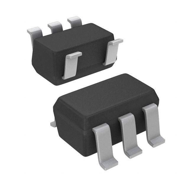
ICGOO电子元器件商城为您提供1P1G126QDBVRQ1由Texas Instruments设计生产,在icgoo商城现货销售,并且可以通过原厂、代理商等渠道进行代购。 1P1G126QDBVRQ1价格参考。Texas Instruments1P1G126QDBVRQ1封装/规格:逻辑 - 缓冲器,驱动器,接收器,收发器, Buffer, Non-Inverting 1 Element 1 Bit per Element 3-State Output SOT-23-5。您可以下载1P1G126QDBVRQ1参考资料、Datasheet数据手册功能说明书,资料中有1P1G126QDBVRQ1 详细功能的应用电路图电压和使用方法及教程。
| 参数 | 数值 |
| 产品目录 | 集成电路 (IC)半导体 |
| 描述 | IC BUS BUFF TRI-ST N-INV SOT23-5缓冲器和线路驱动器 Single Bus Buff Gate W/3-St Otpt |
| 产品分类 | |
| 品牌 | Texas Instruments |
| 产品手册 | |
| 产品图片 |
|
| rohs | 符合RoHS无铅 / 符合限制有害物质指令(RoHS)规范要求 |
| 产品系列 | 逻辑集成电路,缓冲器和线路驱动器,Texas Instruments 1P1G126QDBVRQ174LVC |
| 数据手册 | |
| 产品型号 | 1P1G126QDBVRQ1 |
| 产品目录页面 | |
| 产品种类 | 缓冲器和线路驱动器 |
| 传播延迟时间 | 5.8 ns at 3.3 V, 4.5 ns at 5 V |
| 低电平输出电流 | 24 mA |
| 供应商器件封装 | SOT-23-5 |
| 元件数 | 1 |
| 其它名称 | 1P1G126QDBVRQ1-ND |
| 包装 | 带卷 (TR) |
| 商标 | Texas Instruments |
| 安装类型 | 表面贴装 |
| 安装风格 | SMD/SMT |
| 封装 | Reel |
| 封装/外壳 | SC-74A,SOT-753 |
| 封装/箱体 | SOT-23-5 |
| 工作温度 | -40°C ~ 125°C |
| 工厂包装数量 | 3000 |
| 最大工作温度 | + 125 C |
| 最小工作温度 | - 40 C |
| 极性 | Non-Inverting |
| 标准包装 | 3,000 |
| 每元件位数 | 1 |
| 每芯片的通道数量 | 1 |
| 电压-电源 | 1.65 V ~ 5.5 V |
| 电流-输出高,低 | 24mA,24mA |
| 电源电压-最大 | 5.5 V |
| 电源电压-最小 | 1.65 V |
| 系列 | SN74LVC1G126-Q1 |
| 输入线路数量 | 1 |
| 输出类型 | 3-State |
| 输出线路数量 | 3 |
| 逻辑类型 | 缓冲器/线路驱动器,非反相 |
| 逻辑系列 | LVC |
| 高电平输出电流 | - 24 mA |


- 商务部:美国ITC正式对集成电路等产品启动337调查
- 曝三星4nm工艺存在良率问题 高通将骁龙8 Gen1或转产台积电
- 太阳诱电将投资9.5亿元在常州建新厂生产MLCC 预计2023年完工
- 英特尔发布欧洲新工厂建设计划 深化IDM 2.0 战略
- 台积电先进制程称霸业界 有大客户加持明年业绩稳了
- 达到5530亿美元!SIA预计今年全球半导体销售额将创下新高
- 英特尔拟将自动驾驶子公司Mobileye上市 估值或超500亿美元
- 三星加码芯片和SET,合并消费电子和移动部门,撤换高东真等 CEO
- 三星电子宣布重大人事变动 还合并消费电子和移动部门
- 海关总署:前11个月进口集成电路产品价值2.52万亿元 增长14.8%


PDF Datasheet 数据手册内容提取
SN74LVC1G126-Q1 www.ti.com............................................................................................................................................................. SCES467B–JULY2003–REVISEDAPRIL2008 SINGLE BUS BUFFER GATE WITH 3-STATE OUTPUT FEATURES 1 • QualifiedforAutomotiveApplications DBV PACKAGE • ESDProtectionExceeds2000VPer (TOP VIEW) MIL-STD-883,Method3015;Exceeds200V UsingMachineModel(C=200pF,R=0) OE 1 5 V CC • Supports5-VV Operation A 2 CC • InputsAcceptVoltagesto5.5V GND 3 4 Y • LowPowerConsumption,10-m AMaxI CC • ±24-mAOutputDriveat3.3V • I SupportsPartial-Power-DownMode off Operation • Latch-UpPerformanceExceeds100mAPer JESD78,ClassII DESCRIPTION/ORDERING INFORMATION Thissinglebusbuffergateisdesignedfor1.65-Vto5.5-VV operation. CC The SN74LVC1G126-Q1 is a single line driver with a 3-state output. The output is disabled when the output-enable(OE)inputislow. To ensure the high-impedance state during power up or power down, OE should be tied to GND through a pulldownresistor;theminimumvalueoftheresistorisdeterminedbythecurrent-sourcingcapabilityofthedriver. This device is fully specified for partial-power-down applications using I . The I circuitry disables the outputs, off off preventingdamagingcurrentbackflowthroughthedevicewhenitispowereddown. ORDERINGINFORMATION(1) T PACKAGE(2) ORDERABLEPARTNUMBER TOP-SIDEMARKING(3) A –40(cid:176) Cto125(cid:176) C SOT(SOT-23)–DBV Reelof3000 1P1G126QDBVRQ1 C26_ (1) Forthemostcurrentpackageandorderinginformation,seethePackageOptionAddendumattheendofthisdocument,orseetheTI websiteatwww.ti.com. (2) Packagedrawings,thermaldata,andsymbolizationareavailableatwww.ti.com/packaging. (3) DBV:Theactualtop-sidemarkinghasoneadditionalcharacterthatdesignatesthewaferfab/assemblysite. FUNCTIONTABLE INPUTS OUTPUT OE A Y H H H H L L L X Z 1 Pleasebeawarethatanimportantnoticeconcerningavailability,standardwarranty,anduseincriticalapplicationsof TexasInstrumentssemiconductorproductsanddisclaimerstheretoappearsattheendofthisdatasheet. PRODUCTIONDATAinformationiscurrentasofpublicationdate. Copyright©2003–2008,TexasInstrumentsIncorporated Products conform to specifications per the terms of the Texas Instruments standard warranty. Production processing does not necessarilyincludetestingofallparameters.
SN74LVC1G126-Q1 SCES467B–JULY2003–REVISEDAPRIL2008............................................................................................................................................................. www.ti.com LOGICDIAGRAM(POSITIVELOGIC) 1 OE 2 4 A Y Absolute Maximum Ratings(1) overoperatingfree-airtemperaturerange(unlessotherwisenoted) MIN MAX UNIT V Supplyvoltagerange –0.5 6.5 V CC V Inputvoltagerange(2) –0.5 6.5 V I V Voltagerangeappliedtoanyoutputinthehigh-impedanceorpower-offstate(2) –0.5 6.5 V O V Voltagerangeappliedtoanyoutputinthehighorlowstate(2)(3) –0.5 V +0.5 V O CC I Inputclampcurrent V <0 –50 mA IK I I Outputclampcurrent V <0 –50 mA OK O I Continuousoutputcurrent ±50 mA O ContinuouscurrentthroughV orGND ±100 mA CC q Packagethermalimpedance(4) 206 (cid:176) C/W JA T Storagetemperaturerange –65 150 (cid:176) C stg (1) Stressesbeyondthoselistedunder"absolutemaximumratings"maycausepermanentdamagetothedevice.Thesearestressratings only,andfunctionaloperationofthedeviceattheseoranyotherconditionsbeyondthoseindicatedunder"recommendedoperating conditions"isnotimplied.Exposuretoabsolute-maximum-ratedconditionsforextendedperiodsmayaffectdevicereliability. (2) Theinputandoutputnegative-voltageratingsmaybeexceedediftheinputandoutputcurrentratingsareobserved. (3) ThevalueofV isprovidedintherecommendedoperatingconditionstable. CC (4) ThepackagethermalimpedanceiscalculatedinaccordancewithJESD51-7. 2 SubmitDocumentationFeedback Copyright©2003–2008,TexasInstrumentsIncorporated ProductFolderLink(s):SN74LVC1G126-Q1
SN74LVC1G126-Q1 www.ti.com............................................................................................................................................................. SCES467B–JULY2003–REVISEDAPRIL2008 Recommended Operating Conditions(1) MIN MAX UNIT Operating 1.65 5.5 V Supplyvoltage V CC Dataretentiononly 1.5 V =1.65Vto1.95V 0.65· V CC CC V =2.3Vto2.7V 1.7 CC V High-levelinputvoltage V IH V =3Vto3.6V 2 CC V =4.5Vto5.5V 0.7· V CC CC V =1.65Vto1.95V 0.35· V CC CC V =2.3Vto2.7V 0.7 CC V Low-levelinputvoltage V IL V =3Vto3.6V 0.8 CC V =4.5Vto5.5V 0.3· V CC CC V Inputvoltage 0 5.5 V I V Outputvoltage 0 V V O CC V =1.65V –4 CC V =2.3V –8 CC I High-leveloutputcurrent –16 mA OH V =3V CC –24 V =4.5V –24 CC V =1.65V 4 CC V =2.3V 8 CC I Low-leveloutputcurrent 16 mA OL V =3V CC 24 V =4.5V 24 CC V =1.8V±0.15V,2.5V±0.2V 20 CC Δt/Δv Inputtransitionriseorfallrate V =3.3V±0.3V 10 ns/V CC V =5V±0.5V 5 CC T Operatingfree-airtemperature –40 125 (cid:176) C A (1) AllunusedinputsofthedevicemustbeheldatV orGNDtoensureproperdeviceoperation.RefertotheTIapplicationreport, CC ImplicationsofSloworFloatingCMOSInputs,literaturenumberSCBA004. Copyright©2003–2008,TexasInstrumentsIncorporated SubmitDocumentationFeedback 3 ProductFolderLink(s):SN74LVC1G126-Q1
SN74LVC1G126-Q1 SCES467B–JULY2003–REVISEDAPRIL2008............................................................................................................................................................. www.ti.com Electrical Characteristics overrecommendedoperatingfree-airtemperaturerange(unlessotherwisenoted) PARAMETER TESTCONDITIONS V MIN TYP(1) MAX UNIT CC I =–100m A 1.65Vto5.5V V –0.1 OH CC I =–4mA 1.65V 1.2 OH I =–8mA 2.3V 1.9 OH V V OH I =–16mA 3V 2.4 OH 3V 2.3 I =–24mA OH 4.5V 3.8 I =100m A 1.65Vto5.5V 0.1 OL I =4mA 1.65V 0.45 OL I =8mA 2.3V 0.3 OL V V OL I =16mA 3V 0.4 OL 3V 0.55 I =24mA OL 4.5V 0.55 I AorOEinputs V =5.5VorGND 0to5.5V ±5 m A I I I V orV =5.5V 0 ±10 m A off I O I V =0to5.5V 3.6V 10 m A OZ O I V =5.5VorGND, I =0 1.65Vto5.5V 10 m A CC I O ΔI OneinputatV –0.6V, OtherinputsatV orGND 3Vto5.5V 500 m A CC CC CC C V =V orGND 3.3V 4 pF i I CC (1) AlltypicalvaluesareatV =3.3V,T =25(cid:176) C. CC A Switching Characteristics overrecommendedoperatingfree-airtemperaturerange,C =50pF(unlessotherwisenoted)(seeFigure1) L V =3.3V V =5V CC CC PARAMETER FROM TO ±0.3V ±0.5V UNIT (INPUT) (OUTPUT) MIN MAX MIN MAX t A Y 1 5.8 1 4.5 ns pd t OE Y 1.2 5.8 1 5 ns en t OE Y 1 6 1 4.2 ns dis Operating Characteristics T =25(cid:176) C A TEST VCC=3.3V VCC=5V PARAMETER UNIT CONDITIONS TYP TYP Outputsenabled 19 21 C Powerdissipationcapacitance f=10MHz pF pd Outputsdisabled 3 4 4 SubmitDocumentationFeedback Copyright©2003–2008,TexasInstrumentsIncorporated ProductFolderLink(s):SN74LVC1G126-Q1
SN74LVC1G126-Q1 www.ti.com............................................................................................................................................................. SCES467B–JULY2003–REVISEDAPRIL2008 PARAMETER MEASUREMENT INFORMATION VLOAD From Output RL S1 Open TEST S1 Under Test GND tPLH/tPHL Open (see Note CAL) RL tPLZ/tPZL VLOAD tPHZ/tPZH GND LOAD CIRCUIT INPUTS VCC VI tr/tf VM VLOAD CL RL VD 3.3 V ± 0.3 V 3 V ≤2.5 ns 1.5 V 6 V 50 pF 500 W 0.3 V 5 V ± 0.5 V VCC ≤2.5 ns VCC/2 2 × VCC 50 pF 500 W 0.3 V VI Timing Input VM 0 V tw VI tsu th VI Input VM VM Data Input VM VM 0 V 0 V VOLTAGE WAVEFORMS VOLTAGE WAVEFORMS PULSE DURATION SETUP AND HOLD TIMES VI VI Output Input VM VM Control VM VM 0 V 0 V tPLH tPHL tPZL tPLZ Output VOH Waveform 1 VLOAD/2 Output VM VM VOL (Ss1e ea tN VoLteO ABD) VM VOL + VD VOL tPHL tPLH tPZH tPHZ Output VM VM VOH WSa1v eaOfto uGrtmpNu D2t VM VOH – VD VOH VOL (see Note B) ≈0 V VOLTAGE WAVEFORMS VOLTAGE WAVEFORMS PROPAGATION DELAY TIMES ENABLE AND DISABLE TIMES INVERTING AND NONINVERTING OUTPUTS LOW- AND HIGH-LEVEL ENABLING NOTES: A. CL includes probe and jig capacitance. B. Waveform 1 is for an output with internal conditions such that the output is low, except when disabled by the output control. Waveform2 is for an output with internal conditions such that the output is high, except when disabled by the output control. C. All input pulses are supplied by generators having the following characteristics: PRR ≤ 10 MHz, ZO = 50 W . D. The outputs are measured one at a time, with one transition per measurement. E. tPLZ and tPHZ are the same as tdis. F. tPZL and tPZH are the same as ten. G. tPLH and tPHL are the same as tpd. H. All parameters and waveforms are not applicable to all devices. Figure1.LoadCircuitandVoltageWaveforms Copyright©2003–2008,TexasInstrumentsIncorporated SubmitDocumentationFeedback 5 ProductFolderLink(s):SN74LVC1G126-Q1
PACKAGE OPTION ADDENDUM www.ti.com 11-Apr-2013 PACKAGING INFORMATION Orderable Device Status Package Type Package Pins Package Eco Plan Lead/Ball Finish MSL Peak Temp Op Temp (°C) Top-Side Markings Samples (1) Drawing Qty (2) (3) (4) 1P1G126QDBVRQ1 ACTIVE SOT-23 DBV 5 3000 Green (RoHS CU NIPDAU Level-1-260C-UNLIM -40 to 125 C26O & no Sb/Br) (1) The marketing status values are defined as follows: ACTIVE: Product device recommended for new designs. LIFEBUY: TI has announced that the device will be discontinued, and a lifetime-buy period is in effect. NRND: Not recommended for new designs. Device is in production to support existing customers, but TI does not recommend using this part in a new design. PREVIEW: Device has been announced but is not in production. Samples may or may not be available. OBSOLETE: TI has discontinued the production of the device. (2) Eco Plan - The planned eco-friendly classification: Pb-Free (RoHS), Pb-Free (RoHS Exempt), or Green (RoHS & no Sb/Br) - please check http://www.ti.com/productcontent for the latest availability information and additional product content details. TBD: The Pb-Free/Green conversion plan has not been defined. Pb-Free (RoHS): TI's terms "Lead-Free" or "Pb-Free" mean semiconductor products that are compatible with the current RoHS requirements for all 6 substances, including the requirement that lead not exceed 0.1% by weight in homogeneous materials. Where designed to be soldered at high temperatures, TI Pb-Free products are suitable for use in specified lead-free processes. Pb-Free (RoHS Exempt): This component has a RoHS exemption for either 1) lead-based flip-chip solder bumps used between the die and package, or 2) lead-based die adhesive used between the die and leadframe. The component is otherwise considered Pb-Free (RoHS compatible) as defined above. Green (RoHS & no Sb/Br): TI defines "Green" to mean Pb-Free (RoHS compatible), and free of Bromine (Br) and Antimony (Sb) based flame retardants (Br or Sb do not exceed 0.1% by weight in homogeneous material) (3) MSL, Peak Temp. -- The Moisture Sensitivity Level rating according to the JEDEC industry standard classifications, and peak solder temperature. (4) Multiple Top-Side Markings will be inside parentheses. Only one Top-Side Marking contained in parentheses and separated by a "~" will appear on a device. If a line is indented then it is a continuation of the previous line and the two combined represent the entire Top-Side Marking for that device. Important Information and Disclaimer:The information provided on this page represents TI's knowledge and belief as of the date that it is provided. TI bases its knowledge and belief on information provided by third parties, and makes no representation or warranty as to the accuracy of such information. Efforts are underway to better integrate information from third parties. TI has taken and continues to take reasonable steps to provide representative and accurate information but may not have conducted destructive testing or chemical analysis on incoming materials and chemicals. TI and TI suppliers consider certain information to be proprietary, and thus CAS numbers and other limited information may not be available for release. In no event shall TI's liability arising out of such information exceed the total purchase price of the TI part(s) at issue in this document sold by TI to Customer on an annual basis. OTHER QUALIFIED VERSIONS OF SN74LVC1G126-Q1 : •Catalog: SN74LVC1G126 Addendum-Page 1
PACKAGE OPTION ADDENDUM www.ti.com 11-Apr-2013 •Enhanced Product: SN74LVC1G126-EP NOTE: Qualified Version Definitions: •Catalog - TI's standard catalog product •Enhanced Product - Supports Defense, Aerospace and Medical Applications Addendum-Page 2
PACKAGE MATERIALS INFORMATION www.ti.com 3-Aug-2017 TAPE AND REEL INFORMATION *Alldimensionsarenominal Device Package Package Pins SPQ Reel Reel A0 B0 K0 P1 W Pin1 Type Drawing Diameter Width (mm) (mm) (mm) (mm) (mm) Quadrant (mm) W1(mm) 1P1G126QDBVRQ1 SOT-23 DBV 5 3000 179.0 8.4 3.2 3.2 1.4 4.0 8.0 Q3 PackMaterials-Page1
PACKAGE MATERIALS INFORMATION www.ti.com 3-Aug-2017 *Alldimensionsarenominal Device PackageType PackageDrawing Pins SPQ Length(mm) Width(mm) Height(mm) 1P1G126QDBVRQ1 SOT-23 DBV 5 3000 203.0 203.0 35.0 PackMaterials-Page2
PACKAGE OUTLINE DBV0005A SOT-23 - 1.45 mm max height SCALE 4.000 SMALL OUTLINE TRANSISTOR C 3.0 2.6 0.1 C 1.75 1.45 B A 1.45 MAX PIN 1 INDEX AREA 1 5 2X 0.95 3.05 2.75 1.9 1.9 2 4 3 0.5 5X 0.3 0.15 0.2 C A B (1.1) TYP 0.00 0.25 GAGE PLANE 0.22 TYP 0.08 8 TYP 0.6 0 0.3 TYP SEATING PLANE 4214839/D 11/2018 NOTES: 1. All linear dimensions are in millimeters. Any dimensions in parenthesis are for reference only. Dimensioning and tolerancing per ASME Y14.5M. 2. This drawing is subject to change without notice. 3. Refernce JEDEC MO-178. 4. Body dimensions do not include mold flash, protrusions, or gate burrs. Mold flash, protrusions, or gate burrs shall not exceed 0.15 mm per side. www.ti.com
EXAMPLE BOARD LAYOUT DBV0005A SOT-23 - 1.45 mm max height SMALL OUTLINE TRANSISTOR PKG 5X (1.1) 1 5 5X (0.6) SYMM (1.9) 2 2X (0.95) 3 4 (R0.05) TYP (2.6) LAND PATTERN EXAMPLE EXPOSED METAL SHOWN SCALE:15X SOLDER MASK SOLDER MASK METAL UNDER METAL OPENING OPENING SOLDER MASK EXPOSED METAL EXPOSED METAL 0.07 MAX 0.07 MIN ARROUND ARROUND NON SOLDER MASK SOLDER MASK DEFINED DEFINED (PREFERRED) SOLDER MASK DETAILS 4214839/D 11/2018 NOTES: (continued) 5. Publication IPC-7351 may have alternate designs. 6. Solder mask tolerances between and around signal pads can vary based on board fabrication site. www.ti.com
EXAMPLE STENCIL DESIGN DBV0005A SOT-23 - 1.45 mm max height SMALL OUTLINE TRANSISTOR PKG 5X (1.1) 1 5 5X (0.6) SYMM 2 (1.9) 2X(0.95) 3 4 (R0.05) TYP (2.6) SOLDER PASTE EXAMPLE BASED ON 0.125 mm THICK STENCIL SCALE:15X 4214839/D 11/2018 NOTES: (continued) 7. Laser cutting apertures with trapezoidal walls and rounded corners may offer better paste release. IPC-7525 may have alternate design recommendations. 8. Board assembly site may have different recommendations for stencil design. www.ti.com
IMPORTANTNOTICEANDDISCLAIMER TIPROVIDESTECHNICALANDRELIABILITYDATA(INCLUDINGDATASHEETS),DESIGNRESOURCES(INCLUDINGREFERENCE DESIGNS),APPLICATIONOROTHERDESIGNADVICE,WEBTOOLS,SAFETYINFORMATION,ANDOTHERRESOURCES“ASIS” ANDWITHALLFAULTS,ANDDISCLAIMSALLWARRANTIES,EXPRESSANDIMPLIED,INCLUDINGWITHOUTLIMITATIONANY IMPLIEDWARRANTIESOFMERCHANTABILITY,FITNESSFORAPARTICULARPURPOSEORNON-INFRINGEMENTOFTHIRD PARTYINTELLECTUALPROPERTYRIGHTS. TheseresourcesareintendedforskilleddevelopersdesigningwithTIproducts.Youaresolelyresponsiblefor(1)selectingtheappropriate TIproductsforyourapplication,(2)designing,validatingandtestingyourapplication,and(3)ensuringyourapplicationmeetsapplicable standards,andanyothersafety,security,orotherrequirements.Theseresourcesaresubjecttochangewithoutnotice.TIgrantsyou permissiontousetheseresourcesonlyfordevelopmentofanapplicationthatusestheTIproductsdescribedintheresource.Other reproductionanddisplayoftheseresourcesisprohibited.NolicenseisgrantedtoanyotherTIintellectualpropertyrightortoanythird partyintellectualpropertyright.TIdisclaimsresponsibilityfor,andyouwillfullyindemnifyTIanditsrepresentativesagainst,anyclaims, damages,costs,losses,andliabilitiesarisingoutofyouruseoftheseresources. TI’sproductsareprovidedsubjecttoTI’sTermsofSale(www.ti.com/legal/termsofsale.html)orotherapplicabletermsavailableeitheron ti.comorprovidedinconjunctionwithsuchTIproducts.TI’sprovisionoftheseresourcesdoesnotexpandorotherwisealterTI’sapplicable warrantiesorwarrantydisclaimersforTIproducts. MailingAddress:TexasInstruments,PostOfficeBox655303,Dallas,Texas75265 Copyright©2019,TexasInstrumentsIncorporated