ICGOO在线商城 > 分立半导体产品 > 二极管 - 整流器 - 单 > 1N914B

 Datasheet下载
- 型号: 1N914B
- 制造商: Fairchild Semiconductor
- 库位|库存: xxxx|xxxx
- 要求:
| 数量阶梯 | 香港交货 | 国内含税 |
| +xxxx | $xxxx | ¥xxxx |
查看当月历史价格
查看今年历史价格
1N914B产品简介:
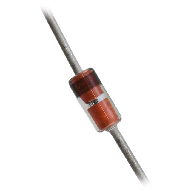
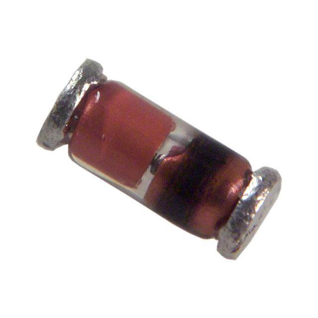
ICGOO电子元器件商城为您提供1N914B由Fairchild Semiconductor设计生产,在icgoo商城现货销售,并且可以通过原厂、代理商等渠道进行代购。 1N914B价格参考。Fairchild Semiconductor1N914B封装/规格:二极管 - 整流器 - 单, 标准 通孔 二极管 100V 200mA DO-35。您可以下载1N914B参考资料、Datasheet数据手册功能说明书,资料中有1N914B 详细功能的应用电路图电压和使用方法及教程。
1N914B是ON Semiconductor公司生产的二极管,属于二极管 - 整流器 - 单类别。它是一款小型信号二极管,广泛应用于各种电子电路中,主要用于信号检波、保护电路和箝位等场合。

 应用场景:

1. 信号检波:
   1N914B常用于无线电接收机中的信号检波电路。它可以将高频交流信号转换为低频直流信号,从而提取出音频或其他有用的信息。由于其快速的开关特性和较低的正向压降,适合处理高频信号。

2. 保护电路:
   在许多电路设计中,1N914B可以用作保护二极管,防止反向电压或瞬态电压对敏感元件造成损害。例如,在电源输入端或传感器接口处,可以使用1N914B来防止电压过冲或极性接反的情况。

3. 箝位电路:
   箝位电路用于限制信号电压在一定范围内,以保护后续电路不受过高或过低电压的影响。1N914B可以作为箝位二极管,确保信号电压不超过设定的安全范围。这种应用常见于模拟电路和数字电路中,特别是在处理高速信号时。

4. 逻辑电平转换:
   在某些情况下,1N914B可以用作简单的逻辑电平转换器。例如,当需要将一个较高电压的信号转换为较低电压的信号时,可以通过1N914B进行电平转换,确保信号完整性的同时避免损坏低电压设备。

5. 脉冲整形:
   1N914B还可以用于脉冲整形电路中,通过调整脉冲的上升沿和下降沿,使其更符合特定的应用需求。这对于定时电路、触发器和其他脉冲信号处理电路非常有用。

6. 开关电源辅助电路:
   在一些开关电源的设计中,1N914B可以用作辅助二极管,帮助吸收开关过程中的尖峰电压,减少电磁干扰(EMI),并提高电源的整体效率和稳定性。

7. 温度补偿电路:
   由于1N914B具有良好的温度特性,它也可以用于温度补偿电路中,帮助稳定电路性能,尤其是在温度变化较大的环境中。

总之,1N914B虽然是一款小型信号二极管,但其广泛应用在多种电子电路中,特别是在需要快速响应、低功耗和高可靠性的场合。
| 参数 | 数值 |
| 产品目录 | |
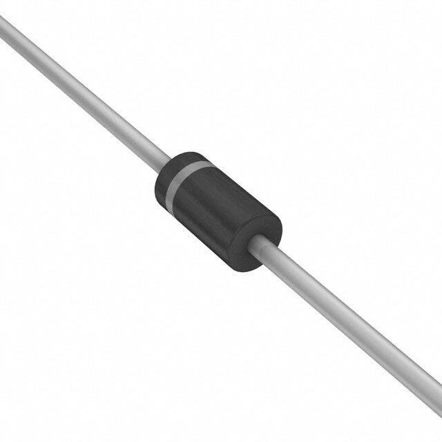
| 描述 | DIODE SMALL SIG 100V 0.2A DO35二极管 - 通用,功率,开关 100V Io/200mA BULK |
| 产品分类 | 单二极管/整流器分离式半导体 |
| 品牌 | Fairchild Semiconductor |
| 产品手册 | |
| 产品图片 |
|
| rohs | RoHS 合规性豁免无铅 / 符合限制有害物质指令(RoHS)规范要求 |
| 产品系列 | 二极管与整流器,二极管 - 通用,功率,开关,Fairchild Semiconductor 1N914B- |
| 数据手册 | |
| 产品型号 | 1N914B |
| PCN封装 | |
| 不同If时的电压-正向(Vf) | 1V @ 100mA |
| 不同 Vr、F时的电容 | 4pF @ 0V,1MHz |
| 不同 Vr时的电流-反向漏电流 | 5µA @ 75V |
| 二极管类型 | 标准 |
| 产品 | Switching Diodes |
| 产品目录页面 | |
| 产品种类 | 二极管 - 通用,功率,开关 |
| 供应商器件封装 | DO-35 |
| 包装 | 散装 |
| 单位重量 | 126 mg |
| 反向恢复时间(trr) | 4ns |
| 商标 | Fairchild Semiconductor |
| 安装类型 | 通孔 |
| 安装风格 | Through Hole |
| 封装 | Bulk |
| 封装/外壳 | DO-204AH,DO-35,轴向 |
| 封装/箱体 | DO-35 |
| 峰值反向电压 | 100 V |
| 工作温度-结 | -65°C ~ 175°C |
| 工厂包装数量 | 2000 |
| 恢复时间 | 4 ns |
| 最大反向漏泄电流 | 5 uA |
| 最大工作温度 | + 175 C |
| 最大浪涌电流 | 4 A |
| 最小工作温度 | - 65 C |
| 标准包装 | 2,000 |
| 正向电压下降 | 1 V at 0.1 A |
| 正向连续电流 | 0.3 A |
| 热阻 | 300°C/W Ja |
| 电压-DC反向(Vr)(最大值) | 100V |
| 电流-平均整流(Io) | 200mA |
| 系列 | 1N914B |
| 速度 | 小信号 =< 200mA(Io),任意速度 |
| 配置 | Single |
| 零件号别名 | 1N914B_NL |


- 商务部:美国ITC正式对集成电路等产品启动337调查
- 曝三星4nm工艺存在良率问题 高通将骁龙8 Gen1或转产台积电
- 太阳诱电将投资9.5亿元在常州建新厂生产MLCC 预计2023年完工
- 英特尔发布欧洲新工厂建设计划 深化IDM 2.0 战略
- 台积电先进制程称霸业界 有大客户加持明年业绩稳了
- 达到5530亿美元!SIA预计今年全球半导体销售额将创下新高
- 英特尔拟将自动驾驶子公司Mobileye上市 估值或超500亿美元
- 三星加码芯片和SET,合并消费电子和移动部门,撤换高东真等 CEO
- 三星电子宣布重大人事变动 还合并消费电子和移动部门
- 海关总署:前11个月进口集成电路产品价值2.52万亿元 增长14.8%


PDF Datasheet 数据手册内容提取
1N4148 / 1N4448 / 1N914B Taiwan Semiconductor 500mW, High Speed Switching Diode FEATURES KEY PARAMETERS ● Low power loss, high efficiency PARAMETER VALUE UNIT ● Ideal for automated placement I 150 mA F ● High surge current capability V 100 V ● Compliant to RoHS directive 2011/65/EU and RRM in accordance to WEEE 2002/96/EC I 2 A FSM ● Halogen-free according to IEC 61249-2-21 V at I =100mA 1 V F F APPLICATIONS TJ MAX 150 °C ● Switching mode power supply (SMPS) Package DO-35 Configuration Singal die MECHANICAL DATA ● Case: DO-35 ● Packing code with suffix "G" means green compound (halogen-free) ● Terminal: Matte tin plated leads, solderable per J-STD-002 ● Polarity: Indicated by cathode band ● Weight: 125 ± 4 mg ABSOLUTE MAXIMUM RATINGS (T = 25°C unless otherwise noted) A PARAMETER SYMBOL 1N4148 1N4448 1N914B UNIT Power dissipation P 500 mW D Repetitive peak reverse voltage V 100 V RRM Non-Repetitive peak forward surge current I 2 A Pluse width = 1μs, Square wave FSM Non-Repetitive peak forward current I 450 mA FM Forward current I 150 mA F Junction temperature range T -65 to +150 °C J Storage temperature range T -65 to +150 °C STG THERMAL PERFORMANCE PARAMETER SYMBOL TYP UNIT Junction-to-ambient thermal resistance R 240 °C/W ӨJA 1 Version:J1804
1N4148 / 1N4448 / 1N914B Taiwan Semiconductor ELECTRICAL SPECIFICATIONS (T = 25°C unless otherwise noted) A PARAMETER CONDITIONS SYMBOL MIN MAX UNIT I = 5 mA, 1N4448,1N914B F 0.62 0.72 T = 25°C J Forward voltage I = 10 mA, 1N4148 F V - 1.00 V per diode (1) T = 25°C F J I = 100 mA, 1N4448,1N914B F - 1.00 T = 25°C J I = 100 μA, T = 25°C 100 - Reverse voltage R J V V (2) R I = 5 μA, T = 25°C 75 - R J V = 20 V, T = 25°C - 25 nA Reverse current R J I (2) R V = 75 V, T = 25°C - 5 μA R J Junction 1 MHz, V =0V C - 4 pF R J capacitance Reverse I = 10mA , V =6V, R = 100Ω , F R L t - 4 ns rr recovery time I = 1mA RR Notes: 1. Pulse test with PW=0.3 ms 2. Pulse test with PW=30 ms ORDERING INFORMATION PART NO. PACKAGE PACKING 1N4148 R0G DO-35 10K / 14" Reel 1N4148 R0 DO-35 10K / 14" Reel 1N4148 A0G DO-35 5K / Box(Ammo) 1N4148 A0 DO-35 5K / Box(Ammo) 1N4448 R0G DO-35 10K / 14" Reel 1N4448 R0 DO-35 10K / 14" Reel 1N4448 A0G DO-35 5K / Box(Ammo) 1N4448 A0 DO-35 5K / Box(Ammo) 1N914B R0G DO-35 10K / 14" Reel 1N914B R0 DO-35 10K / 14" Reel 1N914B A0G DO-35 5K / Box(Ammo) 1N914B A0 DO-35 5K / Box(Ammo) 2 Version:J1804
1N4148 / 1N4448 / 1N914B Taiwan Semiconductor CHARACTERISTICS CURVES (T = 25°C unless otherwise noted) A Fig.1 Typical Forward Characteristics Fig. 2 Reverse Current VS. Reverse Voltage 1 10000 100°C nt (A) 0.1 TA=25°C nA) 1000 70°C Curre nt :l (R d e 100 war Curr 50°C or e F 0.01 s er Rev 10 TA=25°C 0.001 1 0 0.2 0.4 0.6 0.8 1 1.2 1.4 1.6 0 20 40 60 80 100 120 Forward Voltage (V) Reverse Voltage : VR (V) Fig.3 Admissible Power Dissipation Curve Fig.4 Typical Junction Capacitance 500 1.5 W) 400 pF) 1.2 f=1.0 MHz m e ( n ( nc o 300 a 0.9 ati cit p a wer Dissi 200 ction Cap 0.6 o n P u J 100 0.3 0 0 0 25 50 75 100 125 150 175 200 0 5 10 15 20 25 30 Ambient Temperature (oC) Reverse Voltage (V) 3 Version:J1804
1N4148 / 1N4448 / 1N914B Taiwan Semiconductor PACKAGE OUTLINE DIMENSION DO-35 Unit (mm) Unit (inch) DIM. Min Max Min Max A 0.34 0.60 0.013 0.024 B 2.90 5.08 0.114 0.200 C 25.40 38.10 1.000 1.500 D 1.30 2.28 0.051 0.090 MARKING DIAGRAM 4 Version:J1804
1N4148 / 1N4448 / 1N914B Taiwan Semiconductor Notice Specifications of the products displayed herein are subject to change without notice. TSC or anyone on its behalf, assumes no responsibility or liability for any errors or inaccuracies. Information contained herein is intended to provide a product description only. No license, express or implied, to any intellectual property rights is granted by this document. Except as provided in TSC’s terms and conditions of sale for such products, TSC assumes no liability whatsoever, and disclaims any express or implied warranty, relating to sale and/or use of TSC products including liability or warranties relating to fitness for a particular purpose, merchantability, or infringement of any patent, copyright, or other intellectual property right. The products shown herein are not designed for use in medical, life-saving, or life-sustaining applications. Customers using or selling these products for use in such applications do so at their own risk and agree to fully indemnify TSC for any damages resulting from such improper use or sale. 5 Version:J1804
Mouser Electronics Authorized Distributor Click to View Pricing, Inventory, Delivery & Lifecycle Information: T aiwan Semiconductor: 1N914B 1N4148 1N4448 1N4148 R0 1N4148 A0 1N4448 A0 1N914B R0 1N4448 R0 1N4148 R0G 1N4148 A0G 1N4448 R0G 1N4448 A0G 1N914B R0 G