ICGOO在线商城 > 分立半导体产品 > 二极管 - 整流器 - 单 > 1N5820RLG
 Datasheet下载
- 型号: 1N5820RLG
- 制造商: ON Semiconductor
- 库位|库存: xxxx|xxxx
- 要求:
| 数量阶梯 | 香港交货 | 国内含税 |
| +xxxx | $xxxx | ¥xxxx |
查看当月历史价格
查看今年历史价格
1N5820RLG产品简介:
ICGOO电子元器件商城为您提供1N5820RLG由ON Semiconductor设计生产,在icgoo商城现货销售,并且可以通过原厂、代理商等渠道进行代购。 1N5820RLG价格参考。ON Semiconductor1N5820RLG封装/规格:二极管 - 整流器 - 单, 肖特基 通孔 二极管 20V 3A DO-201AD。您可以下载1N5820RLG参考资料、Datasheet数据手册功能说明书,资料中有1N5820RLG 详细功能的应用电路图电压和使用方法及教程。
1N5820RLG 是一款由 ON Semiconductor(安森美半导体)生产的肖特基二极管,属于二极管 - 整流器 - 单类别。它具有低正向电压降和快速开关特性,适用于多种电子电路中。以下是其主要应用场景:

 1. 电源整流
   - 1N5820RLG 可用于直流电源的整流电路中,将交流电转换为直流电。由于其肖特基特性,能够减少能量损耗并提高效率,特别适合低电压、高效率的应用场景。

 2. 逆向保护
   - 在电池供电设备或直流电机驱动电路中,该二极管可以用作反向电流保护器件,防止因电源极性接反导致的电路损坏。

 3. 续流保护
   - 在开关电源、DC-DC 转换器或电机驱动电路中,1N5820RLG 可作为续流二极管,吸收感性负载(如线圈或电机)关断时产生的反电动势,保护开关器件(如 MOSFET 或晶体管)。

 4. 太阳能电池板应用
   - 在小型太阳能发电系统中,该二极管可以防止电池在无光照条件下向太阳能电池板反向放电,同时支持高效的电流传输。

 5. 信号隔离
   - 利用其单向导电性,1N5820RLG 可用于信号隔离电路,确保信号只能在一个方向上传输,避免干扰或回流问题。

 6. 高频电路
   - 因为其快速恢复时间和低正向压降,该二极管非常适合高频整流或开关应用,例如无线充电器、高频逆变器等。

 总结
1N5820RLG 的典型应用场景包括电源管理、保护电路设计以及高效整流需求的场合。它的低功耗和快速响应特性使其成为现代电子设备中不可或缺的元件之一。
| 参数 | 数值 |
| 产品目录 | |
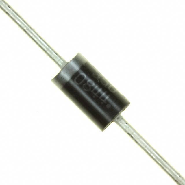
| 描述 | DIODE SCHOTTKY 20V 3A DO201AD肖特基二极管与整流器 3A 20V |
| 产品分类 | 单二极管/整流器分离式半导体 |
| 品牌 | ON Semiconductor |
| 产品手册 | |
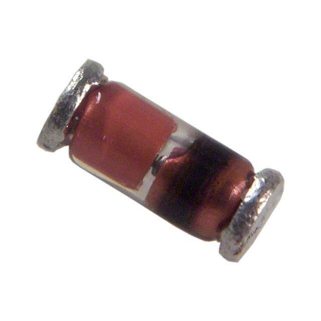
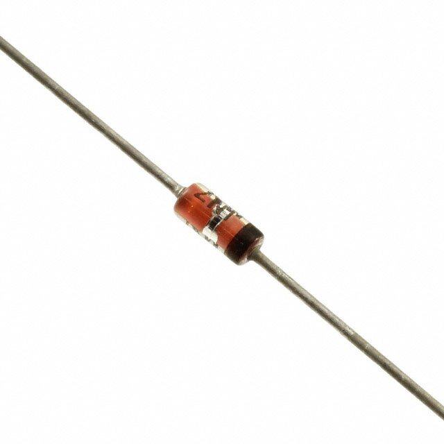
| 产品图片 |
|
| rohs | 符合RoHS无铅 / 符合限制有害物质指令(RoHS)规范要求 |
| 产品系列 | 二极管与整流器,肖特基二极管与整流器,ON Semiconductor 1N5820RLG- |
| 数据手册 | |
| 产品型号 | 1N5820RLG |
| 不同If时的电压-正向(Vf) | 475mV @ 3A |
| 不同 Vr、F时的电容 | - |
| 不同 Vr时的电流-反向漏电流 | 2mA @ 20V |
| 二极管类型 | 肖特基 |
| 产品 | Schottky Diodes |
| 产品目录页面 | |
| 产品种类 | 肖特基二极管与整流器 |
| 供应商器件封装 | DO-201AD |
| 其它名称 | 1N5820RLGOSTR |
| 包装 | 带卷 (TR) |
| 反向恢复时间(trr) | - |
| 商标 | ON Semiconductor |
| 安装类型 | 通孔 |
| 安装风格 | Through Hole |
| 封装 | Reel |
| 封装/外壳 | DO-201AA,DO-27,轴向 |
| 封装/箱体 | DO-201AD |
| 峰值反向电压 | 20 V |
| 工作温度-结 | -65°C ~ 125°C |
| 工作温度范围 | - 65 C to + 125 C |
| 工厂包装数量 | 1500 |
| 技术 | Silicon |
| 最大反向漏泄电流 | 2000 uA |
| 最大工作温度 | + 125 C |
| 最大浪涌电流 | 80 A |
| 最小工作温度 | - 65 C |
| 标准包装 | 1,500 |
| 正向电压下降 | 0.85 V at 9.4 A |
| 正向连续电流 | 3 A |
| 热阻 | 28°C/W Ja |
| 电压-DC反向(Vr)(最大值) | 20V |
| 电流-平均整流(Io) | 3A |
| 系列 | 1N5820 |
| 速度 | 快速恢复 =< 500 ns,> 200mA(Io) |
| 配置 | Single |


PDF Datasheet 数据手册内容提取
1N5820, 1N5821, 1N5822 1N5820 and 1N5822 are Preferred Devices Axial Lead Rectifiers This series employs the Schottky Barrier principle in a large area metal-to-silicon power diode. State-of-the-art geometry features chrome barrier metal, epitaxial construction with oxide passivation and metal overlap contact. Ideally suited for use as rectifiers in low-voltage, high-frequency inverters, free wheeling diodes, and http://onsemi.com polarity protection diodes. Features SCHOTTKY BARRIER • (cid:2)Extremely Low VF RECTIFIERS • (cid:2)Low Power Loss/High Efficiency 3.0 AMPERES • (cid:2)Low Stored Charge, Majority Carrier Conduction 20, 30, 40 VOLTS • (cid:2)Shipped in plastic bags, 500 per bag • (cid:2)Available in Tape and Reel, 1500 per reel, by adding a “RL'' suffix to the part number • (cid:2)Pb-Free Packages are Available* Mechanical Characteristics: • (cid:2)Case: Epoxy, Molded • (cid:2)Weight: 1.1 Gram (Approximately) • (cid:2)Finish: All External Surfaces Corrosion Resistant and Terminal Leads are Readily Solderable • (cid:2)Lead Temperature for Soldering Purposes: 260°C Max. for 10 Seconds AXIAL LEAD •(cid:2)Polarity: Cathode indicated by Polarity Band CASE 267-05 (DO-201AD) STYLE 1 MARKING DIAGRAM A 1N 582x YYWW(cid:2) (cid:2) A = Assembly Location 1N582x = Device Code x = 0, 1, or 2 YY = Year WW = Work Week (cid:2) = Pb-Free Package (Note: Microdot may be in either location) ORDERING INFORMATION See detailed ordering and shipping information on page 3 of this data sheet. Preferred devices are recommended choices for future use *For additional information on our Pb-Free strategy and soldering details, please and best overall value. download the ON Semiconductor Soldering and Mounting Techniques Reference Manual, SOLDERRM/D. ©(cid:2) Semiconductor Components Industries, LLC, 2007 1 Publication Order Number: December, 2007 - Rev. 10 1N5820/D
1N5820, 1N5821, 1N5822 MAXIMUM RATINGS Rating Symbol 1N5820 1N5821 1N5822 Unit Peak Repetitive Reverse Voltage VRRM 20 30 40 V Working Peak Reverse Voltage VRWM DC Blocking Voltage VR Non-Repetitive Peak Reverse Voltage VRSM 24 36 48 V RMS Reverse Voltage VR(RMS) 14 21 28 V Average Rectified Forward Current (Note 1) IO 3.0 A VR(equiv) (cid:2) 0.2 VR(dc), TL = 95°C (R(cid:2)JA = 28°C/W, P.C. Board Mounting, see Note 5) Ambient Temperature TA 90 85 80 °C Rated VR(dc), PF(AV) = 0 R(cid:2)JA = 28°C/W Non-Repetitive Peak Surge Current IFSM 80 (for one cycle) A (Surge applied at rated load conditions, half wave, single phase 60 Hz, TL = 75°C) Operating and Storage Junction Temperature Range TJ, Tstg -65 to +125 °C (Reverse Voltage applied) Stresses exceeding Maximum Ratings may damage the device. Maximum Ratings are stress ratings only. Functional operation above the Recommended Operating Conditions is not implied. Extended exposure to stresses above the Recommended Operating Conditions may affect device reliability. *THERMAL CHARACTERISTICS (Note 5) Characteristic Symbol Max Unit Thermal Resistance, Junction-to-Ambient R(cid:2)JA 28 °C/W *ELECTRICAL CHARACTERISTICS (TL = 25°C unless otherwise noted) (Note 1) Characteristic Symbol 1N5820 1N5821 1N5822 Unit Maximum Instantaneous Forward Voltage (Note 2) VF V (iF = 1.0 Amp) 0.370 0.380 0.390 (iF = 3.0 Amp) 0.475 0.500 0.525 (iF = 9.4 Amp) 0.850 0.900 0.950 Maximum Instantaneous Reverse Current iR mA @ Rated dc Voltage (Note 2) TL = 25°C 2.0 2.0 2.0 TL = 100°C 20 20 20 1. Lead Temperature reference is cathode lead 1/32″ from case. 2. Pulse Test: Pulse Width = 300 (cid:3)s, Duty Cycle =2.0%. *Indicates JEDEC Registered Data for 1N5820-22. http://onsemi.com 2
1N5820, 1N5821, 1N5822 ORDERING INFORMATION Device Package Shipping† 1N5820 Axial Lead 500 Units/Bag 1N5820G Axial Lead 500 Units/Bag (Pb-Free) 1N5820RL Axial Lead 1500/Tape & Reel 1N5820RLG Axial Lead 1500/Tape & Reel (Pb-Free) 1N5821 Axial Lead 500 Units/Bag 1N5821G Axial Lead 500 Units/Bag (Pb-Free) 1N5821RL Axial Lead 1500/Tape & Reel 1N5821RLG Axial Lead 1500/Tape & Reel (Pb-Free) 1N5822 Axial Lead 500 Units/Bag 1N5822G Axial Lead 500 Units/Bag (Pb-Free) 1N5822RL Axial Lead 1500/Tape & Reel 1N5822RLG Axial Lead 1500/Tape & Reel (Pb-Free) †For information on tape and reel specifications, including part orientation and tape sizes, please refer to our Tape and Reel Packaging Specifications Brochure, BRD8011/D. http://onsemi.com 3
1N5820, 1N5821, 1N5822 NOTE 3 — DETERMINING MAXIMUM RATINGS Reverse power dissipation and the possibility of thermal use in common rectifier circuits, Table 1 indicates suggested runaway must be considered when operating this rectifier at factors for an equivalent dc voltage to use for conservative reverse voltages above 0.1 V . Proper derating may be design, that is: RWM accomplished by use of equation (1). V = V (cid:4) F (4) R(equiv) (FM) TA(max) = TJ(max) (cid:3) R(cid:2)JAPF(AV) (cid:3) R(cid:2)JAPR(AV)(1) The factor F is derived by considering the properties of the whereT = Maximum allowable ambient temperature various rectifier circuits and the reverse characteristics of A(max) T = Maximum allowable junction temperature Schottky diodes. J(max) (125°C or the temperature at which thermal EXAMPLE: Find T for 1N5821 operated in a A(max) runaway occurs, whichever is lowest) 12-volt dc supply using a bridge circuit with capacitive filter PF(AV) = Average forward power dissipation such that IDC = 2.0 A (IF(AV) = 1.0 A), I(FM)/I(AV) = 10, Input PR(AV) = Average reverse power dissipation Voltage = 10 V(rms), R(cid:2)JA = 40°C/W. R(cid:2)JA = Junction-to-ambient thermal resistance Step 1. Find VR(equiv). Read F = 0.65 from Table 1, Figures 1, 2, and 3 permit easier use of equation (1) by (cid:5)V = (1.41) (10) (0.65) = 9.2 V. taking reverse power dissipation and thermal runaway into R(equiv) consideration. The figures solve for a reference temperature Step 2. Find TR from Figure 2. Read TR = 108°C as determined by equation (2). @ VR = 9.2 V and R(cid:2)JA = 40°C/W. TR = TJ(max) (cid:3) R(cid:2)JAPR(AV) (2) Step 3. Find PF(AV) from Figure 6. **Read PF(AV) = 0.85 W Substituting equation (2) into equation (1) yields: @II((AFMV))(cid:6)10and(cid:3)IF(AV)(cid:6)1.0(cid:3)A. TA(max) = TR (cid:3) R(cid:2)JAPF(AV) (3) Step 4. Find T from equation (3). A(max) Inspection of equations (2) and (3) reveals that TR is the T = 108 (cid:3) (0.85) (40) = 74°C. A(max) ambient temperature at which thermal runaway occurs or **Values given are for the 1N5821. Power is slightly lower where T = 125°C, when forward power is zero. The J for the 1N5820 because of its lower forward voltage, and transition from one boundary condition to the other is higher for the 1N5822. Variations will be similar for the evident on the curves of Figures 1, 2, and 3 as a difference MBR-prefix devices, using P from Figure 6. in the rate of change of the slope in the vicinity of 115°C. The F(AV) data of Figures 1, 2, and 3 is based upon dc conditions. For Table 1. Values for Factor F Full Wave, Circuit Half Wave Full Wave, Bridge Center Tapped*† Load Resistive Capacitive* Resistive Capacitive Resistive Capacitive Sine Wave 0.5 1.3 0.5 0.65 1.0 1.3 Square Wave 0.75 1.5 0.75 0.75 1.5 1.5 *Note that VR(PK) (cid:7) 2.0 Vin(PK). †Use line to center tap voltage for Vin. http://onsemi.com 4
1N5820, 1N5821, 1N5822 125 125 20 15 20 C) 10 C) 15 °E ( 115 8.0 °E ( 115 10 R R 8.0 U U T T A A R R PE 105 PE 105 EM R(cid:2)JA (°C/W) = 70 EM R(cid:2)JA (°C/W) = 70 T T E E NC 95 50 NC 95 50 RE 40 RE 40 E E EF 28 EF 28 R 85 R 85 , R , R T T 75 75 2.0 3.0 4.0 5.0 7.0 10 15 20 3.0 4.0 5.0 7.0 10 15 20 30 VR, REVERSE VOLTAGE (VOLTS) VR, REVERSE VOLTAGE (VOLTS) Figure 1. Maximum Reference Temperature Figure 2. Maximum Reference Temperature 1N5820 1N5821 125 40 20 MAXIMUM C) 35 °MPERATURE ( 111055 15 10 8.0 RESISTANCE°LEAD ( C/W) 2350 TYPICAL REFERENCE TE 9855 R(cid:2)JA (°C/W) = 70 50 40 R, THERMAL (cid:2)JLJUNCTION-TO- 211050 BOTH LEADS TO HEATSINK, , R 28 5.0 EQUAL LENGTH T 75 0 4.0 5.0 7.0 10 15 20 30 40 0 1/8 2/8 3/8 4/8 5/8 6/8 7/8 1.0 VR, REVERSE VOLTAGE (VOLTS) L, LEAD LENGTH (INCHES) Figure 3. Maximum Reference Temperature Figure 4. Steady-State Thermal Resistance 1N5822 1.0 E The temperature of the lead should be measured using a ther‐ LEAD LENGTH = 1/4″ NC 0.5 mocouple placed on the lead as close as possible to the tie point. TA The thermal mass connected to the tie point is normally large S SI 0.3 enough so that it will not significantly respond to heat surges E THERMAL RRMALIZED) 00..12 gsvTateJe lnu=aee dTr yaoL-tf e s+Tdt a(cid:4)L ,ti enTt h JtceLho ejnu dndicitoitoidonens taeasmr eap earrecashtuuielrtev eomdf a.p yuU lbsseein ddg e ottephreemr aimntieoedna sbouynr:eced tp t1Ppk PpTkIME DPeqEUuATivKYa lPCeOYntCW sLqEEuR a=, r Petp pp/kto1, wise pr epaukls oef. an T O EN(N 0.05 (cid:4)TJL = Ppk • R(cid:2)JL [D + (1 - D) • r(t1 + tp) + r(tp) - r(t1)] where: ANSI 0.03 (cid:4)r(tT) J=L n=o trhmea ilnizcerde avsaelu ien ojufn tcratinosni etenmt tpheerramtuarle r easbisotvaen cthee a lte taimd ete, mt, pi.eer.a:ture. R r(t), T 0.02 rt1(t 1+ +tp t,p e) t=c .normalized value of transient thermal resistance at time 0.01 0.2 0.5 1.0 2.0 5.0 10 20 50 100 200 500 1.0 k 2.0 k 5.0 k 10 k 20 k t, TIME (ms) Figure 5. Thermal Response http://onsemi.com 5
1N5820, 1N5821, 1N5822 S) 10 NOTE 4 - APPROXIMATE THERMAL CIRCUIT MODEL TT 7.0 N (WA 5.0 SI(INFME )WAVE R(cid:2)S(A) R(cid:2)L(A) R(cid:2)J(A) R(cid:2)J(K) R(cid:2)L(K) R(cid:2)S(K) PATIO 32..00 I(AV)(cid:6)(cid:5)(cid:3)(Resistive(cid:3)Load) dc TA(A) PD TA(K) SSI (cid:8) TL(A) TC(A) TJ TC(K) TL(K) R DI 1.0 Capacitive 5.0 SQUARE WAVE E 10 W 0.7 Loads O 20 P 0.5 E Use of the above model permits junction to lead thermal G RA 0.3 resistance for any mounting configuration to be found. For VE 0.2 TJ ≈ 125°C a given total lead length, lowest values occur when one side A , V) of the rectifier is brought as close as possible to the heat sink. F(A 0.1 Terms in the model signify: P 0.1 0.2 0.3 0.5 0.7 1.0 2.0 3.0 5.0 7.0 10 IF(AV), AVERAGE FORWARD CURRENT (AMP) TA = Ambient Temperature TC = Case Temperature T = Lead Temperature T = Junction Temperature Figure 6. Forward Power Dissipation 1N5820-22 L J R(cid:2)S = Thermal Resistance, Heatsink to Ambient R(cid:2)L = Thermal Resistance, Lead-to-Heatsink R(cid:2)J = Thermal Resistance, Junction-to-Case P = Total Power Dissipation = P + P D F R P = Forward Power Dissipation F P = Reverse Power Dissipation R (Subscripts (A) and (K) refer to anode and cathode sides, respectively.) Values for thermal resistance components are: R(cid:2)L = 42°C/W/in typically and 48°C/W/in maximum R(cid:2)J = 10°C/W typically and 16°C/W maximum The maximum lead temperature may be found as follows: T = T (cid:3) (cid:2) T L J(max) JL where (cid:2) TJL (cid:7) R(cid:2)JL · PD Mounting Method 1 Mounting Method 3 P.C. Board where available P.C. Board with NOTE 5 — MOUNTING DATA copper surface is small. 2-1/2, x 2-1/2, copper surface. Data shown for thermal resistance junction-to-ambient (R(cid:2)JA) L L É for the mountings shown is to be used as typical guideline values ÉÉÉÉÉÉÉ É L = 1/2″ for preliminary engineering, or in case the tie point temperature cannot be measured. ÉÉÉÉÉÉÉ É TYPICAL VALUES FOR R(cid:2)JA IN STILL AIR É Mounting Lead Length, L (in) Mounting Method 2 É Method 1/8 1/4 1/2 3/4 R(cid:2)JA ÉÉÉL ÉÉÉL ÉÉ BOARPDL AGNREOUND 1 50 51 53 55 °C/W ÉÉÉÉÉÉÉÉ 2 58 59 61 63 °C/W VECTOR PUSH-IN 3 28 °C/W TERMINALS T-28 http://onsemi.com 6
1N5820, 1N5821, 1N5822 50 100 P) M A 70 30 T ( N E R 50 20 R CU TL = 75°C E f = 60 Hz V TJ = 100°C WA 30 10 F- L A H 7.0 K 20 1 CYCLE P) EA M P URRENT (A 53..00 25°C , IFSM 101.0 2S.0URG3.E0 APP5L.I0ED 7A.T0 RA1T0ED LOA2D0 CON30DITION5S0 70 100 C D NUMBER OF CYCLES R A 2.0 W Figure 8. Maximum Non-Repetitive Surge R FO Current S U EO 1.0 100 N A TANT 0.7 50 TJ = 125°C S N 0.5 20 , IF i 10 100°C 0.3 A) m 5.0 T ( 0.2 REN 2.0 75°C R U C 1.0 E S 0.1 R 0.5 E V E 0.07 , R 0.2 IR 0.1 25°C 0.05 0 0.1 0.2 0.3 0.4 0.5 0.6 0.7 0.8 0.9 1.0 1.1 1.2 1.3 1.4 0.05 1N5820 vF, INSTANTANEOUS FORWARD VOLTAGE (VOLTS) 1N5821 0.02 1N5822 Figure 7. Typical Forward Voltage 0.01 0 4.0 8.0 12 16 20 24 28 32 36 40 VR, REVERSE VOLTAGE (VOLTS) 500 Figure 9. Typical Reverse Current 1N5820 F) 300 p E ( C NOTE 6 — HIGH FREQUENCY OPERATION N A 200 T PACI TJ = 25°C 1N5821 Since current flow in a Schottky rectifier is the result of A f = 1.0 MHz majority carrier conduction, it is not subject to junction di‐ C C, ode forward and reverse recovery transients due to minority 100 carrier injection and stored charge. Satisfactory circuit ana‐ lysis work may be performed by using a model consisting 70 1N5822 of an ideal diode in parallel with a variable capacitance. 0.5 0.7 1.0 2.0 3.0 5.0 7.0 10 20 30 (See Figure 10.) VR, REVERSE VOLTAGE (VOLTS) Figure 10. Typical Capacitance http://onsemi.com 7
1N5820, 1N5821, 1N5822 PACKAGE DIMENSIONS AXIAL LEAD CASE 267-05 (DO-201AD) ISSUE G K A NOTES: 1.DIMENSIONING AND TOLERANCING PER ANSI D Y14.5M, 1982. 1 2 2.CONTROLLING DIMENSION: INCH. INCHES MILLIMETERS DIM MIN MAX MIN MAX A 0.287 0.374 7.30 9.50 B B 0.189 0.209 4.80 5.30 K D 0.047 0.051 1.20 1.30 K 1.000 --- 25.40 --- STYLE 1: PIN 1.CATHODE (POLARITY BAND) 2.ANODE ON Semiconductor and are registered trademarks of Semiconductor Components Industries, LLC (SCILLC). SCILLC reserves the right to make changes without further notice to any products herein. SCILLC makes no warranty, representation or guarantee regarding the suitability of its products for any particular purpose, nor does SCILLC assume any liability arising out of the application or use of any product or circuit, and specifically disclaims any and all liability, including without limitation special, consequential or incidental damages. “Typical” parameters which may be provided in SCILLC data sheets and/or specifications can and do vary in different applications and actual performance may vary over time. All operating parameters, including “Typicals” must be validated for each customer application by customer's technical experts. SCILLC does not convey any license under its patent rights nor the rights of others. SCILLC products are not designed, intended, or authorized for use as components in systems intended for surgical implant into the body, or other applications intended to support or sustain life, or for any other application in which the failure of the SCILLC product could create a situation where personal injury or death may occur. Should Buyer purchase or use SCILLC products for any such unintended or unauthorized application, Buyer shall indemnify and hold SCILLC and its officers, employees, subsidiaries, affiliates, and distributors harmless against all claims, costs, damages, and expenses, and reasonable attorney fees arising out of, directly or indirectly, any claim of personal injury or death associated with such unintended or unauthorized use, even if such claim alleges that SCILLC was negligent regarding the design or manufacture of the part. SCILLC is an Equal Opportunity/Affirmative Action Employer. This literature is subject to all applicable copyright laws and is not for resale in any manner. PUBLICATION ORDERING INFORMATION LITERATURE FULFILLMENT: N. American Technical Support: 800-282-9855 Toll Free ON Semiconductor Website: www.onsemi.com Literature Distribution Center for ON Semiconductor USA/Canada P.O. Box 5163, Denver, Colorado 80217 USA Europe, Middle East and Africa Technical Support: Order Literature: http://www.onsemi.com/orderlit Phone: 303-675-2175 or 800-344-3860 Toll Free USA/Canada Phone: 421 33 790 2910 Fax: 303-675-2176 or 800-344-3867 Toll Free USA/Canada Japan Customer Focus Center For additional information, please contact your local Email: orderlit@onsemi.com Phone: 81-3-5773-3850 Sales Representative http://onsemi.com 1N5820/D 8
Mouser Electronics Authorized Distributor Click to View Pricing, Inventory, Delivery & Lifecycle Information: O N Semiconductor: 1N5820 1N5820G 1N5820RL 1N5820RLG 1N5821 1N5821G 1N5821RL 1N5821RLG 1N5822 1N5822G 1N5822RL 1N5822RLG