ICGOO在线商城 > 分立半导体产品 > 二极管 - 整流器 - 单 > 1N5819G
 Datasheet下载
- 型号: 1N5819G
- 制造商: ON Semiconductor
- 库位|库存: xxxx|xxxx
- 要求:
| 数量阶梯 | 香港交货 | 国内含税 |
| +xxxx | $xxxx | ¥xxxx |
查看当月历史价格
查看今年历史价格
1N5819G产品简介:
ICGOO电子元器件商城为您提供1N5819G由ON Semiconductor设计生产,在icgoo商城现货销售,并且可以通过原厂、代理商等渠道进行代购。 1N5819G价格参考¥1.18-¥1.18。ON Semiconductor1N5819G封装/规格:二极管 - 整流器 - 单, 肖特基 通孔 二极管 40V 1A 轴向。您可以下载1N5819G参考资料、Datasheet数据手册功能说明书,资料中有1N5819G 详细功能的应用电路图电压和使用方法及教程。
| 参数 | 数值 |
| 产品目录 | |
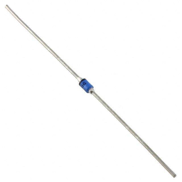
| 描述 | DIODE SCHOTTKY 40V 1A AXIAL肖特基二极管与整流器 1A 40V |
| 产品分类 | 单二极管/整流器分离式半导体 |
| 品牌 | ON Semiconductor |
| 产品手册 | |
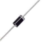
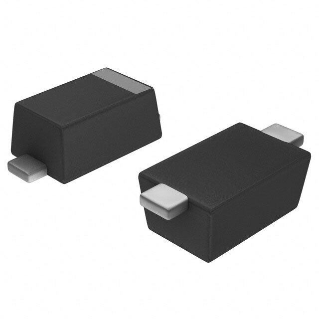
| 产品图片 |
|
| rohs | 符合RoHS无铅 / 符合限制有害物质指令(RoHS)规范要求 |
| 产品系列 | 二极管与整流器,肖特基二极管与整流器,ON Semiconductor 1N5819G- |
| 数据手册 | |
| 产品型号 | 1N5819G |
| 不同If时的电压-正向(Vf) | 600mV @ 1A |
| 不同 Vr、F时的电容 | - |
| 不同 Vr时的电流-反向漏电流 | 1mA @ 40V |
| 二极管类型 | |
| 产品 | Schottky Rectifiers |
| 产品目录页面 | |
| 产品种类 | 肖特基二极管与整流器 |
| 供应商器件封装 | 轴向 |
| 其它名称 | 1N5819G-ND |
| 包装 | 散装 |
| 反向恢复时间(trr) | - |
| 商标 | ON Semiconductor |
| 安装类型 | 通孔 |
| 安装风格 | Through Hole |
| 封装 | Bulk |
| 封装/外壳 | DO-204AL,DO-41,轴向 |
| 封装/箱体 | DO-41 |
| 峰值反向电压 | 40 V |
| 工作温度-结 | -65°C ~ 125°C |
| 工作温度范围 | - 65 C to + 125 C |
| 工厂包装数量 | 1000 |
| 技术 | Silicon |
| 最大反向漏泄电流 | 1000 uA |
| 最大工作温度 | + 125 C |
| 最大浪涌电流 | 25 A |
| 最小工作温度 | - 65 C |
| 标准包装 | 1,000 |
| 正向电压下降 | 0.9 V at 3 A |
| 正向连续电流 | 1 A |
| 热阻 | 80°C/W Ja |
| 电压-DC反向(Vr)(最大值) | 40V |
| 电流-平均整流(Io) | 1A |
| 系列 | 1N5819 |
| 速度 | 快速恢复 =< 500 ns,> 200mA(Io) |
| 配置 | Single |


- 商务部:美国ITC正式对集成电路等产品启动337调查
- 曝三星4nm工艺存在良率问题 高通将骁龙8 Gen1或转产台积电
- 太阳诱电将投资9.5亿元在常州建新厂生产MLCC 预计2023年完工
- 英特尔发布欧洲新工厂建设计划 深化IDM 2.0 战略
- 台积电先进制程称霸业界 有大客户加持明年业绩稳了
- 达到5530亿美元!SIA预计今年全球半导体销售额将创下新高
- 英特尔拟将自动驾驶子公司Mobileye上市 估值或超500亿美元
- 三星加码芯片和SET,合并消费电子和移动部门,撤换高东真等 CEO
- 三星电子宣布重大人事变动 还合并消费电子和移动部门
- 海关总署:前11个月进口集成电路产品价值2.52万亿元 增长14.8%


PDF Datasheet 数据手册内容提取
1N5817, 1N5818, 1N5819 1N5817 and 1N5819 are Preferred Devices Axial Lead Rectifiers This series employs the Schottky Barrier principle in a large area metal−to−silicon power diode. State−of−the−art geometry features chrome barrier metal, epitaxial construction with oxide passivation and metal overlap contact. Ideally suited for use as rectifiers in low−voltage, high−frequency inverters, free wheeling diodes, and http://onsemi.com polarity protection diodes. Features SCHOTTKY BARRIER • Extremely Low V RECTIFIERS F • Low Stored Charge, Majority Carrier Conduction 1.0 AMPERE • Low Power Loss/High Efficiency 20, 30 and 40 VOLTS • These are Pb−Free Devices* Mechanical Characteristics: • Case: Epoxy, Molded • Weight: 0.4 Gram (Approximately) • Finish: All External Surfaces Corrosion Resistant and Terminal Leads are Readily Solderable • Lead Temperature for Soldering Purposes: 260°C Max for 10 Seconds • AXIAL LEAD Polarity: Cathode Indicated by Polarity Band • CASE 59 ESD Ratings: Machine Model = C (>400 V) STYLE 1 Human Body Model = 3B (>8000 V) MARKING DIAGRAM A 1N581x YYWW(cid:2) (cid:2) A =Assembly Location 1N581x =Device Number x= 7, 8, or 9 YY =Year WW =Work Week (cid:2) =Pb−Free Package (Note: Microdot may be in either location) ORDERING INFORMATION See detailed ordering and shipping information on page 6 of this data sheet. *For additional information on our Pb−Free strategy and soldering details, please download the ON Semiconductor Soldering and Mounting Techniques Preferred devices are recommended choices for future use Reference Manual, SOLDERRM/D. and best overall value. © Semiconductor Components Industries, LLC, 2006 1 Publication Order Number: July, 2006 − Rev. 10 1N5817/D
1N5817, 1N5818, 1N5819 MAXIMUM RATINGS Rating Symbol 1N5817 1N5818 1N5819 Unit Peak Repetitive Reverse Voltage VRRM 20 30 40 V Working Peak Reverse Voltage VRWM DC Blocking Voltage VR Non−Repetitive Peak Reverse Voltage VRSM 24 36 48 V RMS Reverse Voltage VR(RMS) 14 21 28 V Average Rectified Forward Current (Note 1), (VR(equiv) ≤ 0.2 VR(dc), TL = 90°C, IO 1.0 A R(cid:2)JA = 80°C/W, P.C. Board Mounting, see Note 2, TA = 55°C) Ambient Temperature (Rated VR(dc), PF(AV) = 0, R(cid:2)JA = 80°C/W) TA 85 80 75 °C Non−Repetitive Peak Surge Current, (Surge applied at rated load conditions, IFSM 25 (for one cycle) A half−wave, single phase 60 Hz, TL = 70°C) Operating and Storage Junction Temperature Range (Reverse Voltage applied) TJ, Tstg −65 to +125 °C Peak Operating Junction Temperature (Forward Current applied) TJ(pk) 150 °C Stresses exceeding Maximum Ratings may damage the device. Maximum Ratings are stress ratings only. Functional operation above the Recommended Operating Conditions is not implied. Extended exposure to stresses above the Recommended Operating Conditions may affect device reliability. THERMAL CHARACTERISTICS (Note 1) Characteristic Symbol Max Unit Thermal Resistance, Junction−to−Ambient R(cid:2)JA 80 °C/W ELECTRICAL CHARACTERISTICS (TL = 25°C unless otherwise noted) (Note 1) Characteristic Symbol 1N5817 1N5818 1N5819 Unit Maximum Instantaneous Forward Voltage (Note 2) (iF = 0.1 A) vF 0.32 0.33 0.34 V (iF = 1.0 A) 0.45 0.55 0.6 (iF = 3.0 A) 0.75 0.875 0.9 Maximum Instantaneous Reverse Current @ Rated dc Voltage (Note 2) IR mA (TL = 25°C) 1.0 1.0 1.0 (TL = 100°C) 10 10 10 1. Lead Temperature reference is cathode lead 1/32 in from case. 2. Pulse Test: Pulse Width = 300 (cid:3)s, Duty Cycle = 2.0%. http://onsemi.com 2
1N5817, 1N5818, 1N5819 NOTE 3. — DETERMINING MAXIMUM RATINGS 125 40 30 23 Reverse power dissipation and the possibility of thermal runaway must be considered when operating this rectifier at C)° 115 reverse voltages above 0.1 VRWM. Proper derating may be E ( R accomplished by use of equation (1). U T TA(max) = TJ(max) − R(cid:2)JAPF(AV) − R(cid:2)JAPR(AV) (1) ERA 105 where TTAJ((mmaaxx)) == MMaaxxiimmuumm aalllloowwaabbllee ajumncbtiieonnt tteemmppeerraattuurree TEMP 95 R(cid:2)JA (°C/W) = 110 (125°C or the temperature at which thermal CE 80 runaway occurs, whichever is lowest) N PF(AV) = Average forward power dissipation ERE 85 60 PR(AV) = Average reverse power dissipation REF R(cid:2)JA = Junction−to−ambient thermal resistance , R T Figures 1, 2, and 3 permit easier use of equation (1) by 75 2.0 3.0 4.0 5.0 7.0 10 15 20 taking reverse power dissipation and thermal runaway into V , DC REVERSE VOLTAGE (VOLTS) R consideration. The figures solve for a reference temperature Figure 1. Maximum Reference Temperature as determined by equation (2). 1N5817 TR = TJ(max) − R(cid:2)JAPR(AV) (2) 125 Substituting equation (2) into equation (1) yields: TA(max) = TR − R(cid:2)JAPF(AV) (3) C)° 115 40 30 23 Inspection of equations (2) and (3) reveals that T is the E ( R R U ambient temperature at which thermal runaway occurs or T A where TJ = 125°C, when forward power is zero. The PER 105 R(cid:2)JA (°C/W) = 110 transition from one boundary condition to the other is M TE 80 evident on the curves of Figures 1, 2, and 3 as a difference E 95 60 in the rate of change of the slope in the vicinity of 115°C. The NC E R data of Figures 1, 2, and 3 is based upon dc conditions. For E F 85 use in common rectifier circuits, Table 1 indicates suggested RE factors for an equivalent dc voltage to use for conservative , R T design, that is: 75 3.0 4.0 5.0 7.0 10 15 20 30 VR(equiv) = Vin(PK) x F (4) VR, DC REVERSE VOLTAGE (VOLTS) The factor F is derived by considering the properties of the Figure 2. Maximum Reference Temperature various rectifier circuits and the reverse characteristics of 1N5818 Schottky diodes. 125 40 EXAMPLE: Find T for 1N5818 operated in a A(max) 12−volt dc supply using a bridge circuit with capacitive filter C)° 30 such that I = 0.4 A (I = 0.5 A), I /I = 10, Input E ( 115 23 DC F(AV) (FM) (AV) R Voltage = 10 V(rms), R(cid:2)JA = 80°C/W. ATU R 105 Step 1. Find VR(equiv). Read F = 0.65 from Table 1, PE R(cid:2)JA (°C/W) = 110 Step 1. Find ∴ VR(equiv) = (1.41)(10)(0.65) = 9.2 V. EM 80 Step 2. Find TR from Figure 2. Read TR = 109°C E T 95 Step 1. Find @ VR = 9.2 V and R(cid:2)JA = 80°C/W. NC 60 Step 3. Find PF(AV) from Figure 4. **Read PF(AV) = 0.5 W RE E I(FM) EF 85 @ = 10 and IF(AV) = 0.5 A. R I(AV) , R T Step 4. Find TA(max) from equation (3). 75 Step 4. Find TA(max) = 109 − (80) (0.5) = 69°C. 4.0 5.0 7.0 10 15 20 30 40 V , DC REVERSE VOLTAGE (VOLTS) R **Values given are for the 1N5818. Power is slightly lower for the Figure 3. Maximum Reference Temperature 1N5817 because of its lower forward voltage, and higher for the 1N5819. 1N5819 Table 1. Values for Factor F Circuit Half Wave Full Wave, Bridge Full Wave, Center Tapped*† Load Resistive Capacitive* Resistive Capacitive Resistive Capacitive Sine Wave 0.5 1.3 0.5 0.65 1.0 1.3 Square Wave 0.75 1.5 0.75 0.75 1.5 1.5 **Note that VR(PK) ≈ 2.0 Vin(PK). †Use line to center tap voltage for Vin. http://onsemi.com 3
1N5817, 1N5818, 1N5819 W) D (C/°90 ATTS) 5.0 Sine Wave O−LEA 80 BOTH ELQEAUDASL LTEON HGETAHTSINK, ON (W 32..00 II((FAMV)) = π (Resistive Load) TION−T 7600 SSIPATI 1.0 CaLpoaacdistive{150 dc JUNC 50 MAXIMUM ER DI 00..75 20 SQUARE WAVE NCE, 40 TYPICAL POW 0.3 T ≈ 125°C A E J SIST 30 RAG 0.2 E E R V THERMAL 2100 1 1/8 1/4 3/8 1/2 5/8 3/4 7/8 1.0 P, AF(AV) 00..000.751 0.2 0.4 0.6 0.8 1.0 2.0 4.0 , L J L, LEAD LENGTH (INCHES) I , AVERAGE FORWARD CURRENT (AMP) θ F(AV) R Figure 4. Steady−State Thermal Resistance Figure 5. Forward Power Dissipation 1N5817−19 D) E Z LI 1.0 A M 0.7 R O 0.5 N E ( 0.3 NC Z(cid:2)JL(t) = Z(cid:2)JL • r(t) A 0.2 T RESIS 0.1 tp Ppk Ppk DPEUATYK CPYOCWLEER, ,D P =p kt,p i/st1 peak of AL 0.07 TIME aenquivalent square power pulse. RM 0.05 t1 HE (cid:4)TJL = Ppk • R(cid:2)JL [D + (1 − D) • r(t1 + tp) + r(tp) − r(t1)] where NT T 00..0032 (cid:4)r(tT) J=L n=o trhmea inlizcereda vsael uine joufn tcrtaionns ietenmt ptheerramtuarle r easbiosvtaen tchee alet atidm tee,m t,p feroramtu Freigure 6, E i.e.: SI AN 0.01 r(t) = r(t1 + tp) = normalized value of transient thermal resistance at time, t1 + tp. R T 0.1 0.2 0.5 1.0 2.0 5.0 10 20 50 100 200 500 1.0k 2.0k 5.0k 10k r(t), t, TIME (ms) Figure 6. Thermal Response Mounting Method 1 Mounting Method 3 NOTE 4. — MOUNTING DATA Data shown for thermal resistance, junction−to−ambient P.C. Board with P.C. Board with 1−1/2″ x 1−1/2″ 1−1/2″ x 1−1/2″ (R(cid:2)JA) for the mountings shown is to be used as typical guide- copper surface. copper surface. line values for preliminary engineering, or in case the tie L = 3/8″ point temperature cannot be measured. L L TYPICAL VALUES FOR R(cid:2)JA IN STILL AIR Lead Length, L (in) Mounting Method 1/8 1/4 1/2 3/4 R(cid:2)JA BOARD GROUND PLANE 1 52 65 72 85 °C/W Mounting Method 2 2 67 80 87 100 °C/W 3 50 °C/W L L VECTOR PIN MOUNTING http://onsemi.com 4
1N5817, 1N5818, 1N5819 NOTE 5. — THERMAL CIRCUIT MODEL (For heat conduction through the leads) R(cid:2)S(A) R(cid:2)L(A) R(cid:2)J(A) R(cid:2)J(K) R(cid:2)L(K) R(cid:2)S(K) TA(A) PD TA(K) TL(A) TC(A) TJ TC(K) TL(K) Use of the above model permits junction to lead thermal re- (Subscripts A and K refer to anode and cathode sides, re- sistance for any mounting configuration to be found. For a spectively.) Values for thermal resistance components are: given total lead length, lowest values occur when one side of R(cid:2)L = 100°C/W/in typically and 120°C/W/in maximum the rectifier is brought as close as possible to the heatsink. R(cid:2)J = 36°C/W typically and 46°C/W maximum. Terms in the model signify: TA = Ambient Temperature TC = Case Temperature TL = Lead Temperature TJ = Junction Temperature R(cid:2)S = Thermal Resistance, Heatsink to Ambient R(cid:2)L = Thermal Resistance, Lead to Heatsink R(cid:2)J = Thermal Resistance, Junction to Case PD = Power Dissipation 30 P) M 20 20 T (A 1 Cycle N RE TL = 70°C R f = 60 Hz 10 U E C 10 7.0 G R 5.0 TC = 100°C SU 7.0 P) AK M E A P 5.0 T ( 3.0 , M N S Surge Applied at E F R 2.0 I Rated Load Conditions R U 25°C 3.0 C 1.0 2.0 3.0 5.0 7.0 10 20 30 40 70 100 D R NUMBER OF CYCLES A 1.0 W R O 0.7 Figure 8. Maximum Non−Repetitive Surge Current F S U 0.5 O E 30 N T = 125°C A 20 J NT 0.3 TA A) 15 , INSF 0.2 NT (m 5.0 100°C i RE 3.0 R 2.0 0.1 CU 75°C E 1.0 0.07 RS E 0.5 V 0.05 RE 0.3 25°C , R 0.2 I 0.03 0.1 1N5817 0.02 0.05 1N5818 0.1 0.2 0.3 0.4 0.5 0.6 0.7 0.8 0.9 1.0 1.1 0.03 1N5819 v, INSTANTANEOUS FORWARD VOLTAGE (VOLTS) 0 4.0 8.0 12 16 20 24 28 32 36 40 F V , REVERSE VOLTAGE (VOLTS) R Figure 7. Typical Forward Voltage Figure 9. Typical Reverse Current http://onsemi.com 5
1N5817, 1N5818, 1N5819 NOTE 6. — HIGH FREQUENCY OPERATION Since current flow in a Schottky rectifier is the result of 200 majority carrier conduction, it is not subject to junction diode forward and reverse recovery transients due to 100 minority carrier injection and stored charge. Satisfactory F) p circuit analysis work may be performed by using a model E ( 70 1N5817 C N 1N5818 consisting of an ideal diode in parallel with a variable A 50 T capacitance. (See Figure 10.) CI 1N5819 A P Rectification efficiency measurements show that A 30 C operation will be satisfactory up to several megahertz. For C, 20 TJ = 25°C example, relative waveform rectification efficiency is f = 1.0 MHz approximately 70 percent at 2.0 MHz, e.g., the ratio of dc power to RMS power in the load is 0.28 at this frequency, 10 whereas perfect rectification would yield 0.406 for sine 0.4 0.6 0.81.0 2.0 4.0 6.08.010 20 40 wave inputs. However, in contrast to ordinary junction VR, REVERSE VOLTAGE (VOLTS) diodes, the loss in waveform efficiency is not indicative of Figure 10. Typical Capacitance power loss: it is simply a result of reverse current flow through the diode capacitance, which lowers the dc output voltage. ORDERING INFORMATION Device Package Shipping† 1N5817 Axial Lead* 1000 Units / Bag 1N5817G Axial Lead* 1000 Units / Bag 1N5817RL Axial Lead* 5000 / Tape & Reel 1N5817RLG Axial Lead* 5000 / Tape & Reel 1N5818 Axial Lead* 1000 Units / Bag 1N5818G Axial Lead* 1000 Units / Bag 1N5818RL Axial Lead* 5000 / Tape & Reel 1N5818RLG Axial Lead* 5000 / Tape & Reel 1N5819 Axial Lead* 1000 Units / Bag 1N5819G Axial Lead* 1000 Units / Bag 1N5819RL Axial Lead* 5000 / Tape & Reel 1N5819RLG Axial Lead* 5000 / Tape & Reel †For information on tape and reel specifications, including part orientation and tape sizes, please refer to our Tape and Reel Packaging Specifications Brochure, BRD8011/D. *This package is inherently Pb−Free. http://onsemi.com 6
1N5817, 1N5818, 1N5819 PACKAGE DIMENSIONS AXIAL LEAD CASE 59−10 ISSUE U NOTES: 1. DIMENSIONING AND TOLERANCING PER ANSI B Y14.5M, 1982. 2. CONTROLLING DIMENSION: INCH. 3. ALL RULES AND NOTES ASSOCIATED WITH JEDEC DO−41 OUTLINE SHALL APPLY 4. POLARITY DENOTED BY CATHODE BAND. 5. LEAD DIAMETER NOT CONTROLLED WITHIN F DIMENSION. K D INCHES MILLIMETERS DIM MIN MAX MIN MAX F A 0.161 0.205 4.10 5.20 B 0.079 0.106 2.00 2.70 D 0.028 0.034 0.71 0.86 A F −−− 0.050 −−− 1.27 K 1.000 −−− 25.40 −−− POLARITY INDICATOR OPTIONAL AS NEEDED F STYLE 1: (SEE STYLES) PIN 1.CATHODE (POLARITY BAND) 2.ANODE K ON Semiconductor and are registered trademarks of Semiconductor Components Industries, LLC (SCILLC). SCILLC reserves the right to make changes without further notice to any products herein. SCILLC makes no warranty, representation or guarantee regarding the suitability of its products for any particular purpose, nor does SCILLC assume any liability arising out of the application or use of any product or circuit, and specifically disclaims any and all liability, including without limitation special, consequential or incidental damages. “Typical” parameters which may be provided in SCILLC data sheets and/or specifications can and do vary in different applications and actual performance may vary over time. All operating parameters, including “Typicals” must be validated for each customer application by customer’s technical experts. SCILLC does not convey any license under its patent rights nor the rights of others. SCILLC products are not designed, intended, or authorized for use as components in systems intended for surgical implant into the body, or other applications intended to support or sustain life, or for any other application in which the failure of the SCILLC product could create a situation where personal injury or death may occur. Should Buyer purchase or use SCILLC products for any such unintended or unauthorized application, Buyer shall indemnify and hold SCILLC and its officers, employees, subsidiaries, affiliates, and distributors harmless against all claims, costs, damages, and expenses, and reasonable attorney fees arising out of, directly or indirectly, any claim of personal injury or death associated with such unintended or unauthorized use, even if such claim alleges that SCILLC was negligent regarding the design or manufacture of the part. SCILLC is an Equal Opportunity/Affirmative Action Employer. This literature is subject to all applicable copyright laws and is not for resale in any manner. PUBLICATION ORDERING INFORMATION LITERATURE FULFILLMENT: N. American Technical Support: 800−282−9855 Toll Free ON Semiconductor Website: www.onsemi.com Literature Distribution Center for ON Semiconductor USA/Canada P.O. Box 5163, Denver, Colorado 80217 USA Europe, Middle East and Africa Technical Support: Order Literature: http://www.onsemi.com/orderlit Phone: 303−675−2175 or 800−344−3860 Toll Free USA/Canada Phone: 421 33 790 2910 Fax: 303−675−2176 or 800−344−3867 Toll Free USA/Canada Japan Customer Focus Center For additional information, please contact your local Email: orderlit@onsemi.com Phone: 81−3−5773−3850 Sales Representative http://onsemi.com 1N5817/D 7
Mouser Electronics Authorized Distributor Click to View Pricing, Inventory, Delivery & Lifecycle Information: O N Semiconductor: 1N5817 1N5817G 1N5817RL 1N5817RLG 1N5818 1N5818G 1N5818RL 1N5818RLG 1N5819 1N5819G 1N5819RL 1N5819RLG