ICGOO在线商城 > 分立半导体产品 > 二极管 - 齐纳 - 单 > 1N5366B-TP
 Datasheet下载
- 型号: 1N5366B-TP
- 制造商: MCC
- 库位|库存: xxxx|xxxx
- 要求:
| 数量阶梯 | 香港交货 | 国内含税 |
| +xxxx | $xxxx | ¥xxxx |
查看当月历史价格
查看今年历史价格
1N5366B-TP产品简介:
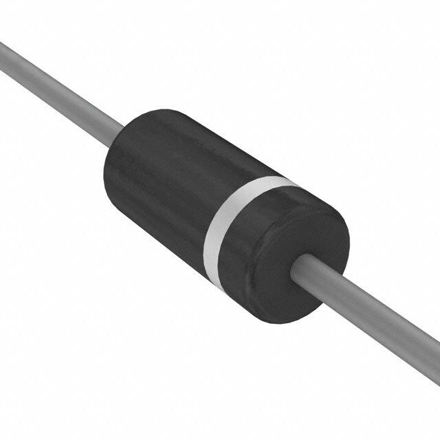
ICGOO电子元器件商城为您提供1N5366B-TP由MCC设计生产,在icgoo商城现货销售,并且可以通过原厂、代理商等渠道进行代购。 1N5366B-TP价格参考。MCC1N5366B-TP封装/规格:二极管 - 齐纳 - 单, Zener Diode 39V 5W ±5% Through Hole DO-15。您可以下载1N5366B-TP参考资料、Datasheet数据手册功能说明书,资料中有1N5366B-TP 详细功能的应用电路图电压和使用方法及教程。
| 参数 | 数值 |
| 产品目录 | |
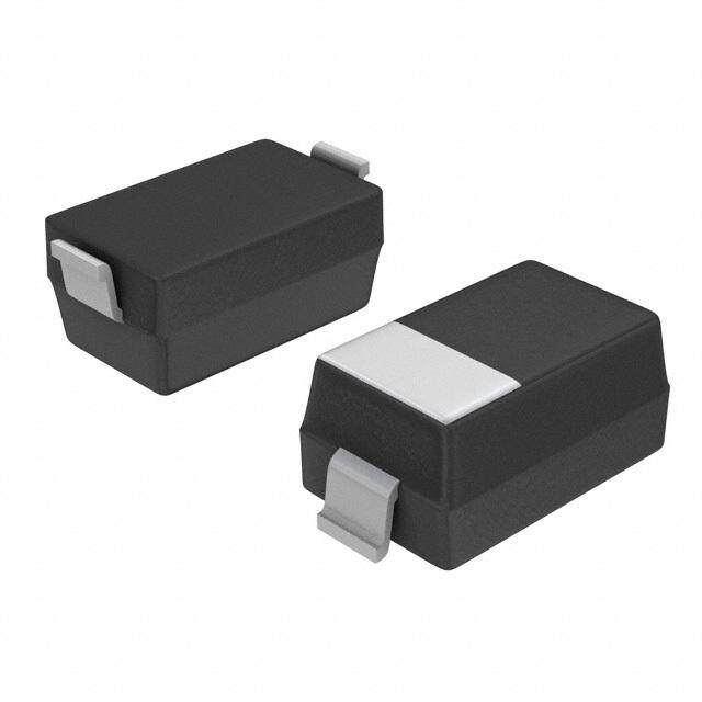
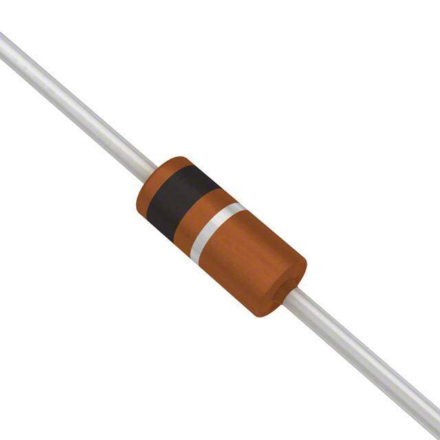
| 描述 | DIODE ZENER 39V 5W DO15 |
| 产品分类 | 单二极管/齐纳 |
| 品牌 | Micro Commercial Co |
| 数据手册 | |
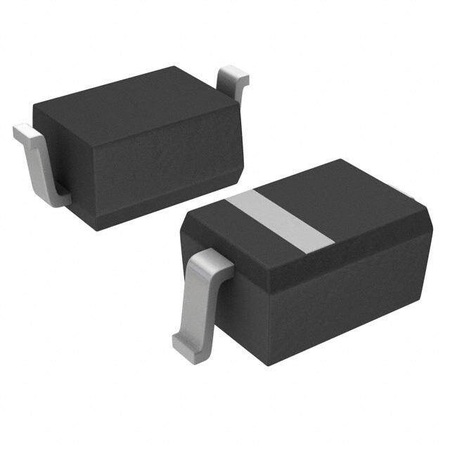
| 产品图片 |
|
| 产品型号 | 1N5366B-TP |
| rohs | 无铅 / 符合限制有害物质指令(RoHS)规范要求 |
| 产品系列 | - |
| 不同If时的电压-正向(Vf) | 1.2V @ 1A |
| 不同 Vr时的电流-反向漏电流 | 500nA @ 29.7V |
| 产品培训模块 | http://www.digikey.cn/PTM/IndividualPTM.page?site=cn&lang=zhs&ptm=24932 |
| 产品目录绘图 |
|
| 供应商器件封装 | DO-15 |
| 其它名称 | 1N5366BTPMSCT |
| 功率-最大值 | 5W |
| 包装 | 剪切带 (CT) |
| 安装类型 | 通孔 |
| 容差 | ±5% |
| 封装/外壳 | DO-204AC,DO-15,轴向 |
| 工作温度 | -55°C ~ 150°C |
| 标准包装 | 1 |
| 电压-齐纳(标称值)(Vz) | 39V |
| 阻抗(最大值)(Zzt) | 14 欧姆 |


- 商务部:美国ITC正式对集成电路等产品启动337调查
- 曝三星4nm工艺存在良率问题 高通将骁龙8 Gen1或转产台积电
- 太阳诱电将投资9.5亿元在常州建新厂生产MLCC 预计2023年完工
- 英特尔发布欧洲新工厂建设计划 深化IDM 2.0 战略
- 台积电先进制程称霸业界 有大客户加持明年业绩稳了
- 达到5530亿美元!SIA预计今年全球半导体销售额将创下新高
- 英特尔拟将自动驾驶子公司Mobileye上市 估值或超500亿美元
- 三星加码芯片和SET,合并消费电子和移动部门,撤换高东真等 CEO
- 三星电子宣布重大人事变动 还合并消费电子和移动部门
- 海关总署:前11个月进口集成电路产品价值2.52万亿元 增长14.8%

PDF Datasheet 数据手册内容提取
1N5338B M C C THRU (cid:1)(cid:2)(cid:3)(cid:4)(cid:5)(cid:6)(cid:7)(cid:5)(cid:8)(cid:8)(cid:9)(cid:4)(cid:3)(cid:2)(cid:10)(cid:11)(cid:6)(cid:7)omponents TM 20736 Marilla Street Chatsworth 1N5388B Micro Commercial Components (cid:7)(cid:12)(cid:6)(cid:13)(cid:14)(cid:15)(cid:14)(cid:14) (cid:16)(cid:17)(cid:5)(cid:18)(cid:9)(cid:19)(cid:6)(cid:20)(cid:21)(cid:14)(cid:21)(cid:22)(cid:6)(cid:23)(cid:24)(cid:14)(cid:25)(cid:26)(cid:13)(cid:15)(cid:15) (cid:27)(cid:10)(cid:28)(cid:19)(cid:6)(cid:6)(cid:6)(cid:20)(cid:21)(cid:14)(cid:21)(cid:22)(cid:6)(cid:23)(cid:24)(cid:14)(cid:25)(cid:26)(cid:13)(cid:15)(cid:13) Features 5 Watt (cid:120)(cid:3) Zener Voltage From 5.1V to 200V • Epoxy meets UL 94 V-0 flammability rating Zener Diode • Moisture Sensitivity Level 1 • Lead Free Finish/RoHS Compliant (Note1) ("P"Suffix designates 5.1 to Volts 200 Compliant. See ordering information) • Marking : Cathode band and type number • Halogen free available upon request by adding suffix "-HF" Maximum Ratings: DO-15 (cid:120)(cid:3) Operating Temperature: -55(cid:113)C to +150(cid:113)C (cid:120)(cid:3) Storage Temperature: -55(cid:113)C to +150(cid:113)C (cid:120)(cid:3) 5 Watt DC Power Dissipation (cid:120)(cid:3) Maximum Forward Voltage @ 1A: 1.2 Volts (cid:120)(cid:3) Power Derating: 67 mW/(cid:1082) Above 75(cid:1082) (cid:120)(cid:3) Maximum thermal resistence: 15oC/W from junction to lead 83OC/W from junction to ambient D Mechanical Data Case: JEDEC DO-15. Terminals: Solder plated , solderable per MIL-STD-750, Method 2026. A Standard Packaging: 52mm tape Cathode Mark B D C DIMENSIONS INCHES MM DIM MIN MAX MIN MAX NOTE A .230 .300 5.80 7.60 B .104 .140 2.60 3.60 C .026 .034 .70 .90 D 1.000 --- 25.40 --- Note: 1. High Temperature Solder Exemption Applied, see EU Directive Annex 7. www.mccsemi.com Revision: 20 E 1 of 6 14/02/26
M C C TM 1N5338B THRU 1N5388B Micro Commercial Components ELECTRICALCHARACTERISTICS(TA=25(cid:113)Cunlessotherwisenoted,VF=1.2Max@IF=1Aforalltypes) MAXIMUM MAXIMUM MAXIMUM MAXIMUM MAXIMUM REGULATOR TEST TEST DYNAMIC MAXIMUM DYNAMIC REVERSE REGULATOR SURGE MCC PART VOLTAGE CURRENT VOLTAGE KNEE VOLTAGE IMPEDANCE CURRENT CURRENT CURRENT NUMBER VZ IZ VR IMPEDANCE REGULATION ZZT IR IZM IZSM ZZK@1.0mA VOLTS mA OHMS (cid:358)A VOLTS mA OHMS A VOLTS 1N5338B 5.1 240 1.5 1 1 930 400 14.4 0.39 1N5339B 5.6 220 1 1 2 865 400 13.4 0.25 1N5340B 6 200 1 1 3 790 300 12.7 0.19 1N5341B 6.2 200 1 1 3 765 200 12.4 0.1 1N5342B 6.8 175 1 10 5.2 700 200 11.5 0.15 1N5343B 7.5 175 1.5 10 5.7 630 200 10.7 0.15(cid:23)(cid:0)(cid:20)(cid:0)(cid:27) 1N5344B 8.2 150 1.5 10 6.2 580 200 10 0.2 1N5345B 8.7 150 2 10 6.6 545 200 9.5 0.2 1N5346B 9.1 150 2 7.5 6.9 520 150 9.2 0.22 1N5347B 10 125 2 5 7.6 475 125 8.6 0.22 1N5348B 11 125 2.5 5 8.4 430 125 8 0.25 1N5349B 12 100 2.5 2 9.1 395 125 7.5 0.25 1N5350B 13 100 2.5 1 9.9 365 100 7 0.25 1N5351B 14 100 2.5 1 10.6 340 75 6.7 0.25 1N5352B 15 75 2.5 1 11.5 315 75 6.3 0.25 1N5353B 16 75 2.5 1 12.2 295 75 6 0.3 1N5354B 17 70 2.5 0.5 12.9 280 75 5.8 0.35 1N5355B 18 65 2.5 0.5 13.7 264 75 5.5 0.4 1N5356B 19 65 3 0.5 14.4 250 75 5.3 0.4 1N5357B 20 65 3 0.5 15.2 237 75 5.1 0.4 1N5358B 22 50 3.5 0.5 16.7 216 75 4.7 0.45 1N5359B 24 50 3.5 0.5 18.2 198 100 4.4 0.55 1N5360B 25 50 4 0.5 19 190 110 4.3 0.55 1N5361B 27 50 5 0.5 20.6 176 120 4.1 0.6 1N5362B 28 50 6 0.5 21.2 170 130 3.9 0.6 1N5363B 30 40 8 0.5 22.8 158 140 3.7 0.6 1N5364B 33 40 10 0.5 25.1 144 150 3.5 0.6 1N5365B 36 30 11 0.5 27.4 132 160 3.3 0.65 1N5366B 39 30 14 0.5 29.7 122 170 3.1 0.65 1N5367B 43 30 20 0.5 32.7 110 190 2.8 0.7 1N5368B 47 25 25 0.5 35.8 100 210 2.7 0.8 1N5369B 51 25 27 0.5 38.8 93 230 2.5 0.9 1N5370B 56 20 35 0.5 42.6 86 280 2.3 1 1N5371B 60 20 40 0.5 45.5 79 350 2.2 1.2 1N5372B 62 20 42 0.5 47.1 76 400 2.1 1.35 1N5373B 68 20 44 0.5 51.7 70 500 2 1.5 1N5374B 75 20 45 0.5 56 63 620 1.9 1.6 1N5375B 82 15 65 0.5 62.2 58 720 1.8 1.8 1N5376B 87 15 75 0.5 66 54.5 760 1.7 2 1N5377B 91 15 75 0.5 69.2 52.5 760 1.6 2.2 1N5378B 100 12 90 0.5 76 47.5 800 1.5 2.3 1N5379B 110 12 125 0.5 83.6 43 1000 1.4 2.5 1N5380B 120 10 170 0.5 91.2 39.5 1150 1.3 2.5 1N5381B 130 10 190 0.5 98.8 36.6 1250 1.2 2.5 1N5382B 140 8 230 0.5 106 34 1500 1.2 2.5 1N5383B 150 8 330 0.5 114 31.6 1500 1.1 3 1N5384B 160 8 350 0.5 122 29.4 1650 1.1 3 1N5385B 170 8 380 0.5 129 28 1750 1 3 1N5386B 180 5 430 0.5 137 26.4 1750 1 4 1N5387B 190 5 450 0.5 144 25 1850 0.9 5 1N5388B 200 5 480 0.5 152 23.6 1850 0.9 5 NOTE: 1.TOLERANCEANDVOLTAGEDESIGNATION-TheJEDECtypenumbersshownindicateatoleranceof+/-10%with guaranteed limits on only Vz, I ,I , and V as shown in the electrical characteristics table. Units with guaranteed limits R r F on all seven parameters are indicated by suffix “B” for+/-5% tolerance. 2.ZENERVOLTAGE(Vz)ANDIMPEDANCE(Z &Z )- TestconditionsforZener voltageandimpedanceareas ZT ZK follows;Izisapplied40+/-10mspriortoreading.Mountingcontactsarelocatedfromtheinsideedgeofmounting clips to the body of the diode(Ta=25oC) www.mccsemi.com Revision: E 2014/02/26 2 of 6
M C C TM Micro Commercial Components 1N5338B THRU 1N5388B 3.SURGECURRENT(Ir)-Surgecurrentisspecifiedasthemaximumallowablepeak,non-recurrentsquare-wave currentwithapulsewidth,PW,of8.3ms.ThedatagiveninFigure5maybeusedtofindthemaximumsurge currentforaquarewaveofanypulsewidthbetween1msand1000msbyplottingtheapplicablepointson logarithmic paper. Examples of this, using the 6.8v , is shown in Figure 6. Mounting contactlocatedasspecifiedinNote3.(TA=25(cid:263)). 4.VOLTAGEREGULATION(Vz)-Testconditionsforvoltageregulationareasfollows:Vzmeasurementsaremade at10% andthenat50%oftheIzmaxvaluelistedintheelectricalcharacteristicstable.Thetestcurrentsarethe sameforthe5% and10%tolerancedevices.ThetestcurrenttimedruationforeachVzmeasurementis40+/-10ms. (T =25C).MountingcontactlocatedasspecifiedinNote2. A 5.MAXIMUMREGULATORCURRENT(I )-Themaximumcurrentshownisbasedonthemaximumvoltageof a ZM 5% typeunit.Therefore,itappliesonlytotheB-suffixdevice.TheactualI foranydevicemaynotexceedthe ZM valueof5wattsdividedbytheactualVzofthedevice.T =75Catmaximumfromthedevicebody. L APPLICATION NOTE: Since the actual voltage available from a given Zener For worst‐case design, using expected limits of I , limits Z diode is temperature dependent, it is necessary to determine of P and the extremes of T ((cid:2)T ) may be estimated. D J J junction temperature under any set of operating conditions Changes in voltage, V , can then be found from: Z in order to calculate its value. The following procedure is (cid:2)V = (cid:4) (cid:2)T VZ J recommended: (cid:4) , the Zener voltage temperature coefficient, is found Lead Temperature, T , should be determined from: VZ L from Figures 2 and 3. T = (cid:4) P + T L LA D A Under high power‐pulse operation, the Zener voltage will (cid:4) is the lead‐to‐ambient thermal resistance and P is the LA D vary with time and may also be affected significantly by the power dissipation. zener resistance. For best regulation, keep current Junction Temperature, T , may be found from: J excursions as low as possible. T = T + (cid:2)T Data of Figure 4 should not be used to compute surge J L JL (cid:2)T is the increase in junction temperature above the lead capability. Surge limitations are given in Figure 5. They are JL lower than would be expected by considering only junction temperature and may be found from Figure 4 for a train of temperature, as current crowding effects cause temperatures power pulses or from Figure 1 for dc power. to be extremely high in small spots resulting in device (cid:2)T = (cid:4) P JL JL D degradation should the limits of Figure 5 be exceeded. www.mccsemi.com Revision: E 3 o f 6 2014/02/26
M C C RATING ANDCHARACTERISTICSCURVES TM Micro Commercial Components 1N5338B THRU 1N5388B TEMPERATURECOEFFICIENTS S) T T A W ON ( NT 300 ATI CIE 200 ER DISSIP 86 RE COEFFI@ IZT1530000 RANGE POW 4 RATU°V/C) 2100 UMU 2 EMPE(m 5 MAXI 0 V, TZ 0 20 40 60 80 100 120 140 160 180 200 220 PD, 0 20 40 60 80 100 120 140 160 θ VZ,ZENERVOLTAGE@IZT(VOLTS) TL,LEADTEMPERATURE Fig.1-POWERTEMPERATUREDERATING CURVE Fig.2-TEMPERATURECOEFFICIENT-RANGEFORUNITS CE 6TO 51VOLTS N A T 20 S ESIW) 10 D = 0.5 RMAL R°AD (C/ 5 D = 0.2 PPK t1 RANSIENT THENCTION‐TO‐LE 0.521 DDD === 000...00151 NNOOTTEE:: BREELSOPWON 0S.1E SCEUCROVNED I,S T AHPEPRLMICAALBLE REPETITISVIEN GPULELS PEUDSL US (cid:2)TEY T(cid:2) JC LTY =JCL (cid:4)L =JE L(cid:4),( tDJ,L D(=t)) PPt1PP/tKK2 t2 TU D), J D = 0 NOTE: TO ANY LEAD LENGTH (L). (t, L 0.20.001 0.005 0.01 0.05 0.1 0.5 1 5 10 20 50 100 J θ t, TIME (SECONDS) Figure 3. Typical Thermal Response L, Lead Length = 3/8 Inch MAL PS) 40 ER AM 20 PW=1ms* D THW) 40 NT ( 10 PW=8.3ms* CTION-TO -LEAESISTANCE(C/ 32 100 0 MCOOUPNPTERONPA8D.0SmTmO2 SURGE CURRE 0.4421 PW=1000ms* UNR EACHTERMINAL AK 0.2 SINE/SQUAREWAVEPW=100ms* JL, J 0 0 0.2 0.4 0.6 0.8 1 R, PE 0.13 4 6 8 10 20 30 40 60 80100 200 I L,LEADLENGTHTOHEATSINK(INCH) NOMINALVZ(V) Fig.4-TYPICALTHERMALRESISTANCE Fig.5-MAXIMUMNON-REPETITIVESURGE CURRENTVERSUSNOMINALZENER VOLTAGE(SEENOTE3) www.mccsemi.com Revision: E 4 o f 6 2014/02/26
M C C RATING ANDCHARACTERISTICSCURVES TM Micro Commercial Components 1N5338B THRU 1N5388B ZENERVOLTAGEVERSUSZENERCURRENT (FIGURES7,8) 30 MPS) 20 VZ=6.8V A) TC=25 T=25 A 10 m 1000 RENT ( 5 PLOTTEDFROMINFORMATION ENT ( 100 UR 2 GIVEN IN FIGURE 5 RR C U GE 1 R C 10 R E U 0.5 N S E 1 K Z , PEAr 00..211 10 100 1000 IZ, 0.11 2 3 4 5 6 7 8 9 10 I VZ,ZENERVOLTAGE(VOLTS) Fig.6-PEAKSURGECURRENT VERSUSPULSE Fig.7-ZENERVOLTAGEVERSUSZENERCURRENT WIDTH(SEENOTE3) VZ=6.8THRU10VOLTS 1000 A) T=25 m T ( 100 N E R UR 10 C R E N ZE 1 IZ, 0.1 10 20 30 40 50 60 70 80 VZ,ZENERVOLTAGE(VOLTS) Fig.8-ZENERVOLTAGEVERSUSZENERCURRENT VZ =11THRU51VOLTS ***DataofFigure3shouldnotbeusedtocomputesurgecapability.SurgelimitationsaregiveninFigure5.Theyare lowerthanwouldbeexpectedbyconsideringonlyjunctiontemperature,ascurrentcrowdingeffectscause temperaturestobeextremelyhighinsmallspotsresultingindevicedegradationshouldthelimitsof Figure.5be exceeded www.mccsemi.com Revision: E 5 o f 6 2014/02/26
M C C TM Micro Commercial Components Ordering Information : Device Packing Part Number-TP Tape&Reel: 4Kpcs/Reel Part Number-AP Ammo Packing: 3Kpcs/Ammo Box Part Number-BP Bulk: 25Kpcs/Carton Note : Adding "-HF" suffix for halogen free, eg. Part Number-TP-HF ***IMPORTANT NOTICE*** Micro Commercial Components Corp. reserves the right to make changes without further notice to any product herein to make corrections, modifications , enhancements , improvements , or other changes . Micro Commercial Components Corp . does not assume any liability arising out of the application or use of any product described herein; neither does it convey any license under its patent rights ,nor the rights of others . The user of products in such applications shall assume all risks of such use and will agree to hold Micro Commercial Components Corp . and all the companies whose products are represented on our website, harmless against all damages. ***LIFE SUPPORT*** MCC's products are not authorized for use as critical components in life support devices or systems without the express written approval of Micro Commercial Components Corporation. ***CUSTOMER AWARENESS*** Counterfeiting of semiconductor parts is a growing problem in the industry. Micro Commercial Components (MCC) is taking strong measures to protect ourselves and our customers from the proliferation of counterfeit parts. MCC strongly encourages customers to purchase MCC parts either directly from MCC or from Authorized MCC Distributors who are listed by country on our web page cited below. Products customers buy either from MCC directly or from Authorized MCC Distributors are genuine parts, have full traceability, meet MCC's quality standards for handling and storage. MCC will not provide any warranty coverage or other assistance for parts bought from Unauthorized Sources. MCC is committed to combat this global problem and encourage our customers to do their part in stopping this practice by buying direct or from authorized distributors. www.mccsemi.com 6 of 6 Revision: E 2014/02/26 3